Thermionic and photo-excited electron emission for energy-conversion processes
 Patrick T. McCarthy
 Ronald G. Reifenberger2
  Timothy S. Fisher
- 1Birck Nanotechnology Center, School of Mechanical Engineering, Purdue University, West Lafayette, IN, USA
- 2Birck Nanotechnology Center, School of Physics, Purdue University, West Lafayette, IN, USA
This article describes advances in thermionic and photo-emission materials and applications dating back to the work on thermionic emission by Guthrie (1873) and the photoelectric effect by Hertz (1893). Thermionic emission has been employed for electron beam generation from Edison’s work with the light bulb to modern day technologies such as scanning and transmission electron microscopy. The photoelectric effect has been utilized in common devices such as cameras and photocopiers while photovoltaic cells continue to be widely successful and further researched. Limitations in device efficiency and materials have thus far restricted large-scale energy generation sources based on thermionic and photoemission. However, recent advances in the fabrication of nanoscale emitters suggest promising routes for improving both thermionic and photo-enhanced electron emission along with newly developed research concepts, e.g., photonically enhanced thermionic emission. However, the abundance of new emitter materials and reduced dimensions of some nanoscale emitters increases the complexity of electron-emission theory and engender new questions related to the dimensionality of the emitter. This work presents derivations of basic two and three-dimensional thermionic and photo-emission theory along with comparisons to experimentally acquired data. The resulting theory can be applied to many different material types regardless of composition, bulk, and surface structure.
Historical Introduction
Electron emission as a method of energy generation has been studied for nearly two centuries deriving from a foundation of early research in cathode ray tubes, metal-based field emission, and the photoelectric effect. Over the course of the last century, many advances have occurred in the field leading to applications in microscopy and other forms of material characterization, consumer to advanced optical cameras, among many others. This review focuses on electron emission as a method of electrical power generation, beginning with a brief historical background, but is not meant to be a complete review of electron-emission processes. In particular, field-emission processes as a method of electrical power generation are largely neglected except to facilitate discussions and theoretical derivations related to thermionic and photoemission. Field-emission devices and applications have undergone extensive research and advancements over the last century. Readers interested in learning more about field-emission studies are encouraged to explore citations provided within this document, including but not limited to work on the fundamental theory of field emission by Fowler and Nordheim (Fowler and Nordheim, 1928; Fowler, 1931), reviews by Good et al. (Good and Muller, 1956; Murphy and Good, 1956), and recent work by Jensen et al. (Jensen, 2007a,b). The paper includes derivation of a general formulation for thermionic and photo-emission theory in both three- and two-dimensional emitters. Additionally, discussion of more recent advancements include work in semiconductor-based photovoltaic and nanoscale materials and devices, as the effect of nanoscale dimensions is a subject of significant contemporary research.
Early Thermionic Emission Research
Research on thermionic emission dates back to 1853, when Becquerel (1853) first detected electrical current passing between two platinum wires, one hot and one cold, kept in a variety of gases. Becquerel was studying the electrical conductivity of gases but did not fully recognize the impact of thermal energy at the electrode on electrical current generation. Many others contributed to the understanding of thermionic emission in the late nineteenth century, not the least of which was Guthrie who in 1873 published his work on the relationship between heat and static electricity. Guthrie (1873) measured the discharge of a positively charged, red-hot sphere into air, helping establish understanding of the thermionic emission phenomenon. Later in the nineteenth century, Elster and Geitel (Angrist, 1976) would investigate sealed devices in which electric current was generated between two electrodes, one hot and one cold, measured utilizing an electrometer. Many of these early studies provided the foundations for cathode and x-ray tubes. Crookes and Hittorf (Crookes, 1896) were the foremost pioneers at developing and studying cathode rays, and their research was critical to the present understanding of thermionic emission, as well as the fourth state of matter – plasma.
While research on thermionic emission continued through the ensuing decades, many of the significant advances in thermionic emission, dedicated toward energy generation, occurred in the 1950s. In 1956, Murphy and Good (1956) published a rigorous study of thermionic and field-emission theory, and Hatsopoulos (Hatsopoulos and Kaye, 1958) presented new thermionic converter types while performing theoretical and experimental work on a thermoelectron engine. The interested reader should consult Angrist’s book (Angrist, 1976) on direct energy conversion that provides more details on the history of thermionic emission, along with a detailed thermodynamic analysis of the theory underlying thermionic emission and associated energy generation.
Early Photo-Emission Research
The foundations of photoemission largely derive from Albert Einstein’s Nobel Prize winning work on the quantum theory of the photoelectric effect. However, it was not until the late 1920s that modern photo-emission theory began to take shape. Much of the theory of photo-emission derives from field-emission studies, and no work was more critical to field-emission research than that performed by Fowler (1931) and Fowler and Nordheim (1928) on electron emission induced by high-intensity electric fields. Their studies led to the work performed by DuBridge (1933) in which the effect of temperature on photoelectron energy distributions was quantified. The pioneering work performed by these researchers generated a surge of interest in photoemission, but applying photo-emission theory to newly developed materials proved difficult, as the phenomenon is fundamentally difficult to interpret owing to dependencies on surface structure and material properties that are often challenging to measure.
Starting in the late 1950s and spanning over nearly four decades, Spicer, often in collaboration with Berglund (Berglund and Spicer, 1964a,b; Spicer and Herreragomez, 1993), advanced the understanding of experimental photoemission via a three-step model. The process is described by (1) photoexcitation of an electron, (2) electron motion through the material, and (3) escape of electrons over the surface barrier and into vacuum. Much of this work was dedicated to the theory and applications of photocathodes and provided deeper understanding of critical photo-emission processes such as electron scattering and quantum yield. Both Spicer and Berglund sought a more complete understanding of how absorption and scattering mechanisms influence photoemission in the hope that experimentalists could better interpret their data.
More recently, Jensen has reported many advances in the understanding of photoemission, both theoretically and experimentally. Examples of this work include the development of more rigorous photo-emission models (Jensen et al., 2006a), and experimentally derived wavelength-dependent quantum efficiencies (electrons emitted per photon of illumination) (Jensen et al., 2006b) for metals and coated materials during field and photoemission. This work incorporates the extreme complexity involved in field and photo-emission processes by including thermal effects, surface conditions, illumination source parameters, reflectivity, penetration depth, and scattering rates (amongst others), all in order to quantify accurately electron current distributions and quantum efficiencies. Possibly most useful to researchers in the electron-emission area is his recent work deriving a general formulation for thermal, field, and photo-induced electron emission, bridging the gaps between the three electron-emission processes (Jensen, 2007b).
Electron-Emission Theory
This section provides a complete theory of thermionic and photo electron emission from two- and three-dimensional materials under the parabolic conduction band approximation. Important features of the electron energy distribution are highlighted to facilitate experimental comparisons, including special features related to the spectral breadth of the photoexcitation. This section presents electron-emission theory with a Landauer transmission function formalism, which allows for more straightforward derivations and inclusion of low-dimensional effects than most historical treatments [e.g., Bergeret et al. (1985)].
Electron emission from a material surface occurs through three main possible processes; photoemission, thermionic emission, and field emission (Jensen, 2007b). Photoemission occurs when an electron absorbs photonic energy allowing the electron to emit above the vacuum level. Thermionic emission is a process where thermal energy causes a broadening of the electron distribution such that some higher energy electrons will emit into vacuum. Field emission is a quantum mechanical process in which electrons are able to tunnel through the surface barrier under high electric fields (Murphy and Good, 1956). Figure 1 displays a general energy diagram highlighting the three types of electron emission in which ϕ refers to the work function, which is the energy that an electron must gain above the Fermi energy (EF) in order to emit into vacuum. Though combinations of all three types of emission are possible, they are typically studied separately.
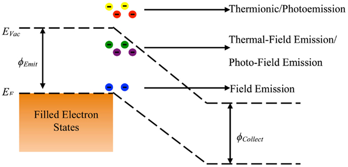
Figure 1. Energy diagram for electron emission from metals.
When establishing criteria for characterizing the quality of fabricated materials, underlying theory must be well developed and understood. While simplified, three-dimensional thermionic emission theory is well established photo-emission theory is often complicated, requiring understanding of a material’s surface and electronic properties. As two-dimensional emission may occur from nanoscale materials, two-dimensional thermionic and photo-emission theories are explored here, and comparisons to three-dimensional theories are discussed. Fitting of electron-emission theory to experimental data allows for precise characterization of the critical parameters related to electron emission, thereby allowing for direct comparisons between different material types.
Electron Current Density
Derivations of two and three-dimensional thermionic and photo-emission theory are briefly described here, but for more detailed derivations the interested reader should review work by Fisher (2013) and McCarthy (2013). General electron flux equation provides the best foundation for deriving thermionic and photo-emission equations. A general form for electron flux was developed by Gadzuk and Plummer (1973) and is described in Landauer form as Fisher (2013):
where J is the electrical current density, E is electron energy, qe is the magnitude of electron charge, vg(E) is the electron group velocity, DdD(E) is the electron density of states for a dimensionality dD, T(E) is the transmission function which accounts for the probability of electron transport through the device, and fFD(T) is the Fermi–Dirac electron distribution function. For simplicity, the group velocity and density of states in Eq. 1 are replaced by the electron mode density to create a general expression for electron density (Fisher, 2013):
where ℏ is the reduced Planck’s constant (h/2π), and MdD(E) is the electron mode density for a dimensionality dD.
To derive thermionic current density from this equation, the temperature at the second state is assumed to be so low that no current flows from state two to state one, such that Eq. 2 is approximated as:
The Fermi–Dirac electron distribution function is defined as:
where kB is Boltzmann’s constant (8.62 × 10⁻⁵ eV/K), and μ is the electrochemical potential of the emitter. For a parabolic conduction band with edge Ec, the number of modes is described by:
where H is the Heaviside step function, gv is the electronic band degeneracy, Wx is the width, and me is the electron mass. In this study, Ec is taken to be zero, gv is taken to be unity, and me = 9.11 × 10⁻³¹ kg (Fisher, 2013).
To develop electron-emission theory fully, the transmission function must be derived. A general form for free-electron metals has been developed (Fisher, 2013) as:
where ϕ is the work function. In this study, μ is considered equivalent to the EF.
When evaluating Eq. 3, Fermi–Dirac statistics are typically replaced with Maxwell–Boltzmann statistics when ϕ ≫ kB T, a condition that is almost always valid. For a three-dimensional emitter, the thermionic current density can be calculated by substituting Eqs 7 and 8 into Eq. 3, resulting in:
Integral evaluation results in the well-known Richardson–Dushman equation (Murphy and Good, 1956).
Semiconductor current density
A promising method of electron energy generation is that of photon-enhanced thermionic emission (PETE) (Schwede et al., 2010). PETE combines photovoltaic based photoemission and thermionic emission processes allowing for conversion of photon energy directly to emitted electron energy, while simultaneously utilizing thermalization and photon absorption losses to drive thermionic emission from electrons excited above the emitter band gap. The PETE concept is discussed in detail later in the report. Because a PETE device utilizes semiconductor materials as opposed to metal emitters often used in thermionic emission, here we extend the foregoing analysis of thermionic electronic emission from metals to semiconductors. Transferring into a symmetric k-space, the three-dimensional thermionic current density from an emitter at temperature T can be expressed as (Fisher, 2013):
where Tθ is the θ-dependent transmission function, and θ is the k-space polar angle. We assume that the transmission is independent of the azimuthal angle, resulting in the simplification:
Assuming classical behavior, an electron will emit when its energy associated with the emission direction (i.e., θ = 0) exceeds the vacuum energy Evac (Fisher, 2013):
where H is the Heaviside function, Ec is the lowest energy of the conduction band, m* is the effective mass in the parabolic band approximation, and Evac is the vacuum energy level (see Figure 2).
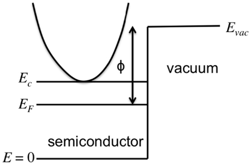
Figure 2. Energy level diagram for a semiconductor with a parabolic conduction band next to vacuum.
Letting x ≡ cos2θ, the angular differential becomes:
The current density can then be expressed as:
The Heaviside function can be used to redefine the integration limits, and the (−) sign can reverse the direction of integration in x:
where
The integrand in Eq. 16 essentially requires that E(k) > (Evac − Ec) through the Heaviside function, and if this condition is satisfied, the integral is performed for values of cos2θ between [(Evac − Ec)/E(k)] and unity, which corresponds to a condition of sufficient energy associated with the surface normal direction for emission to occur.
Evaluation of the integral over x reveals:
The total electron energy is E = E(k) + Ec, and the integrated transmission function becomes:
The current density expression of Eq. 18 converts to an energy integral as:
Incorporation of the expressions for transmission function (Eq. 19) and mode density (Eq. 7) into the current density integral reveals:
By assumption, the vacuum energy level is greater than the conduction band edge (i.e., Evac > Ec), and therefore, the Heaviside functions can be eliminated by changing the lower integration limit to give the final expression for thermionic current density:
For most circumstances, Evac − EF ≫ kB T, allowing the replacement of the Fermi–Dirac distribution function with the simpler Maxwell–Boltzmann function so that the integral can be evaluated analytically:
Notably, this result is identical to that for thermionic emission from free-electron metals with m* as the electron mass (Fisher, 2013).
The resulting current density (Eq. 23) differs from that reported by Schwede et al. (2010) for thermalized electrons emitting from the conduction band such as is found in a PETE device. Their current density is derived for electrons centered at a quasi-Fermi level EF,n that is elevated in energy relative to the standard Fermi level. The resulting current density then becomes:
Comparing results for a GaN sample similar to that utilized by Schwede et al. and taking m* = 0.5 me, T = 500 K, and ϕ = 0.9 eV, then for (EF,n − EF) = 0.3 eV, the semiconductor current density of Eq. 23 is 0.013 A/cm2 while the current density predicted by Eq. 24 is 13.0 A/cm2 – a three order of magnitude increase. The increase in current density resulting from electrons thermalized in the conduction band is significant, particularly for low temperatures (<1500 K). Figure 3 provides a comparison of current densities over a temperature range of 500–2500 K. Thermionic current density (Eq. 10), semiconductor current density derived here (Eq. 23), and PETE type current density derived elsewhere (Schwede et al., 2010) (Eq. 24) are plotted for m* = 0.5 me, ϕ = 0.9 eV, and (EF,n − EF) = 0.1 eV. The PETE theory demonstrates an increased current density relative to pure thermionic emission at low temperatures. The PETE device will also have additional current generated by photo-conversion of electrons, directly emitting out to vacuum and therefore not described by Eq. 24. However, thermionic current density will overtake PETE-based emission at elevated temperatures, assuming all other values stay constant.
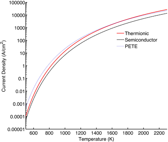
Figure 3. Current densities resulting from thermionic current density (Eq. 10), semiconductor current density (Eq. 23), and PETE type current density (Eq. 24) for m* = 0.5 me, ϕ = 0.9 eV, and (EF,n − EF) = 0.1 eV.
Electron Energy Distribution from a Three-Dimensional Material
The electron-emission intensity for a given energy is defined as:
where EED is the electron energy distribution of emission. By substituting Eq. 3 into Eq. 25 and evaluating, we define the thermionic EED (TEED) as:
Having a generalized equation for thermionic electron emission, dimension-specific equations can also be developed.
An equation for the three-dimensional TEED has been developed elsewhere (McMullen, 2010; Westover et al., 2010) but is re-derived here by substituting Eqs 7 and 8 with d = 3 into Eq. 26 such that:
A simple photo-emission model is developed here following work by Fowler and DuBridge (Fowler and Nordheim, 1928; DuBridge, 1933) and offers a generalized approach for predicting photoemission by ignoring specific material properties. As with the thermionic theory of Eq. 27, this model assumes a free-electron gas with a single parabolic energy band. The model also assumes that photon absorption is independent of photon energy and that all photon energy is converted into electron energy corresponding to momentum in the normal direction. Given these assumptions, the electron population energy distribution is simply increased by the photon energy, and the photo-emission EED (PEED) becomes (Vander Laan, 2011):
where ℏω is the photon energy. This model neglects photonic flux and assumes that all electrons are elevated to a higher energy equivalent to the photon energy. Eq. 28 is termed the “normal energy” model.
An alternative model was developed by Westover (2008) and Vander Laan (2011) as an extension of the theory developed by Fowler and DuBridge that modifies the normal model (Fowler, 1931) by weighting the number of electrons available for emission based on the angle of electron emission. The full derivation is provided here for clarification and to facilitate the two-dimensional derivation provided later.
The derivation closely follows work by Fowler (1931). To begin, a gas of electrons obeying Fermi–Dirac statistics has a distribution per unit volume with velocity components in the ranges u, u + du, v, v + dv, and w, w + dw, with u being the velocity component normal to the surface:
where n(u,v,w) is the electron velocity distribution based on its three-dimensional components. A distribution of electrons based on velocity in the normal direction and in the range of u, u + du is described by:
Figure 4 contains the top half of a polar coordinate system for three dimensions with angles (θp, ϕp) where θp is the polar angle from the surface normal and ϕp is the azimuthal angle in the surface of the plane. Converting to radial coordinates in the plane encompassing the velocity components of v and w, Eq. 30 can be rewritten as:
where ρ2 = v2 + w2, v = ρcos(ϕp), and w = ρsin(ϕp). Eq. 31 is solved analytically to produce:
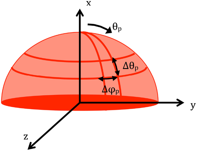
Figure 4. Three-dimensional polar coordinate system for photonic illumination.
The energy associated with the velocity direction normal to the surface is defined as:
Substitution of Eq. 33 in Eq. 32 gives a distribution of electrons based on their energy associated with velocity in the normal direction such that:
When developing the random energy model (REM), Eq. 34 must be expanded to account for the absorbed photon of energy hω. The resulting expression becomes:
where Ψp(θp,ϕp) is the probability that an electron gains energy ℏω in the direction (θp,ϕp). As a probability, the sum of Ψp across the entire solid angle must equal unity, such that:
For clarity, Ψp is assumed to be independent of direction, and therefore, Ψp = 1/4π. Simplifying Eq. 35 gives:
If θp is then discretized into N small segments of angle interval Δθp, then the remaining integral simplifies to:
To obtain an expression for the number of electrons available for emission, Eq. 37 must be integrated over W to find all electrons with energy associated with velocity in the normal direction such that W + ℏωcos(θp) > EF + ϕ. The resulting expression for the total number of electrons available for emission for a given angle θp is:
Eq. 39 is solved numerically, at which point the REM PEED for all dimensions is:
where the total number of electrons available for emission and the θ-dependent PEED for three-dimensional emission are described by:
For a broad-band illumination source, such as a solar simulator, Eq. 40 is integrated over all photon energies such that:
where α is the coefficient of photon absorption that is assumed to be constant for normalized PEEDs, and Iphot(ℏω) is the photon irradiance defined as the number of photons per unit time per unit area. For data fitting purposes, Iphot(ℏω) is normalized with respect to its peak intensity prior to inclusion in Eq. 43. Because the theory does not strictly account for photon flux, all data fitting is performed with normalized peak intensities, and total emission currents are not considered.
Thermionic and Photoemission from Two-Dimensional Materials
An expression for two-dimensional thermionic emission is produced by substituting Eq. 6 and 8 with d = 2 into Eq. 25 and evaluating such that:
When comparing to the three-dimensional TEED, a E1/2 dependence exists in the numerator. A normal energy PEED for two-dimensional theory is once again derived by shifting the Fermi–Dirac function in the TEED such that:
The two-dimensional REM is derived by the same method utilized for three-dimensional theory. We exclude most of the details for the two-dimensional derivation in the interest of brevity.
Ψp is once again assumed to be independent of direction, resulting in Ψp = 1/2π for two dimensions. The resulting expression for the total number of electrons available for emission is thus:
where Γ is the energy associated with velocity in the transverse direction. θp is again discretized into N small segments of angle interval Δθp, and Eq. 46 is solved numerically. The PEED can again be defined by Eq. 40 and 41 where:
For a broad-band solar simulator, Eq. 43 still applies.
Electron Scattering by Optical Phonons
Eq. 43 predicts a PEED that is broader than that typically observed in experiments, particularly for three-dimensional theory. The broad theoretical distribution relative to experimental PEEDs may be a result of scattered electrons that are not accounted for in the theory. One means of accounting for scattering effects was developed by Sun et al. (2011) who modified photo-emission theory by accounting for electron scattering via optical phonons. Low-energy acoustic phonons do not significantly reduce electron-emission energy; therefore, their contributions are ignored.
The assumption underlying the model is that electrons are only scattered by optical phonons, all of which have the same energy. For each scattering event, a reduction of electron energy equivalent to the phonon energy takes place. Electrons can experience multiple scattering events, and the probability of an electron being scattered n times and still emitting follows a Poisson distribution. The modification to the original REM PEED can then be described by Sun et al. (2011):
where Eph is the photon energy. Eq. 48 gives the emission intensity contribution to energy E by electrons originally with higher energy E′ that have been scattered by optical phonons and as a result emit with energy E. In this calculation, electrons are assumed to scatter with equal probability. Here, n = (E′ − E)/Eph, where contributions to an energy level E are only evaluated at an energy level E′such that n is a positive integer; m is taken to be the maximum number of scattering events an electron at energy E′ can encounter and still emit. While this term can be solved for m going to infinity, the higher m terms are ignored so that contributions of electrons with final energies outside of the original PEED are not included in the results (Sun et al., 2011). An integral of all scattering contributions added to the original REM PEED provides the final REM PEED. μs is the mean number of scattering events that an emitted electron experiences, and C(n) is a probability normalization coefficient used to conserve the number of electrons emitted and is defined by:
Figure 5 contains a plot of a normalized PEED from nitrogen-doped diamond films excited by 340 nm light at room temperature (RT) originally presented by Sun et al. (2011). The normal photo-emission model does not capture the experimental distribution shape and peak location, but the addition of scattering by optical phonons leads to a close fit. When fitting to experimental data, uncertainties arising from electron energy detection must be included. Because some variation is allowed in the exact energy of the electrons during detection, a Gaussian instrument function centered on the desired electron energy range describes the extent to which an EED is “smeared” by the detector. The Gaussian instrument function is given by Reifenberger et al. (1979):
where Eo is the center energy value of the recorded EED and σ is the analyzer resolution. When performing data fitting, the theory must account for the Gaussian instrument function of the detector. The final theoretical model should therefore be a convolution Eq. 50 and the thermionic or photo-emission theory of choice.
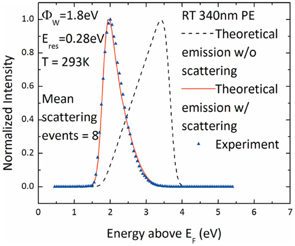
Figure 5. Normalized PEED from nitrogen-doped diamond films. The original theory is three-dimensional normal from Eq. 28 and convolved with the Gaussian instrument function. The theory without scattering has a much higher peak energy and broader distribution. Adding scatter by optical phonons leads to a closer fit to the experimental PEED. Reprinted with permission from Sun et al. (2011).
For further clarification of the impact that scattering has on the PEED, Figure 6 provides a plot of a three-dimensional REM PEED with ϕ = 1.5 eV, T = 500 K, EF = 5.0 eV, and σ = 66 meV for μs = 0, 2, 4, 6, 8, and 10. No scattering events produces a broad PEED with peak energy near 2.2 eV. However, for μs = 2 the PEED is already substantially narrowed, and peak energy is shifted down to approximately 1.7 eV. As μs is further increased, the PEED narrows, and the peak energy decreases, but at a reduced rate owing to the exponential term in Eq. 48.
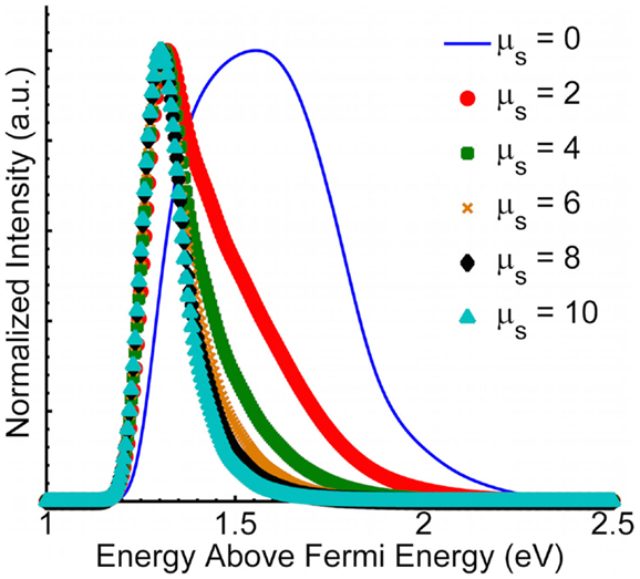
Figure 6. REM PEED for varying μs with ϕ = 1.5 eV, T = 500 K, EF = 5.0 eV, and σ = 66 meV.
Dimensional Dependence on Experimentally Acquired EEDs
In this section, we compare basic EEDs acquired from graphene petals (McCarthy, 2013; McCarthy et al., 2013) to the models above, with particular attention to low-dimensional effects that are expected to appear for thin graphitic emitters. MATLAB computational software (MATLAB 2011b, 2011) was utilized for fitting electron-emission theory to experimental data derived from potassium-intercalated graphitic petals. Theoretical thermionic and PEEDs exhibit strong dimensional dependencies. The square-root dependence on electron energy in the numerator of the two-dimensional emission theory (see Eqs 44 and 45) produces a narrowing of the resulting energy distribution along with a decrease of the peak emission energy when compared to three-dimensional energy distributions.
This phenomenon is evident in Figure 7. The left plot of Figure 7 contains a comparison of two-dimensional and three-dimensional thermionic theory when sample parameters are kept the same: ϕ = 2.5 eV, T = 1280 K, and σ = 0.08 eV. The right plot in Figure 7 is of two-dimensional and three-dimensional thermionic fits to an experimental TEED for thermionic emission from graphitic petals at 1123 K (McCarthy, 2013). The estimated parameters from data fitting are provided in Table 1. A distinct narrowing of the distribution occurs for the same parameter values for two-dimensional emission compared to three-dimensional in the left plot in Figure 7. The narrowing is not apparent in the right plot as the fit allows for T to change, and an increased temperature relative to the three-dimensional fit causes a broadening of the distribution that offsets any narrowing caused by reduced dimensionality. A slight lowering of the peak energy is also apparent. The residual, Rx, in Table 1 is taken to be:
where yexp and yfit are the normalized intensity values of the experimental data and theoretical fit respectively, and n is the number of data points for the EED.
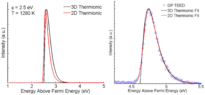
Figure 7. Example three-dimensional and two-dimensional TEEDs from theory (left) with ϕ = 2.5 eV, T = 1280 K, σ = 0.08 eV, and from data fitting (right) to an experimental TEED from graphitic petals at a temperature of 1123 K.
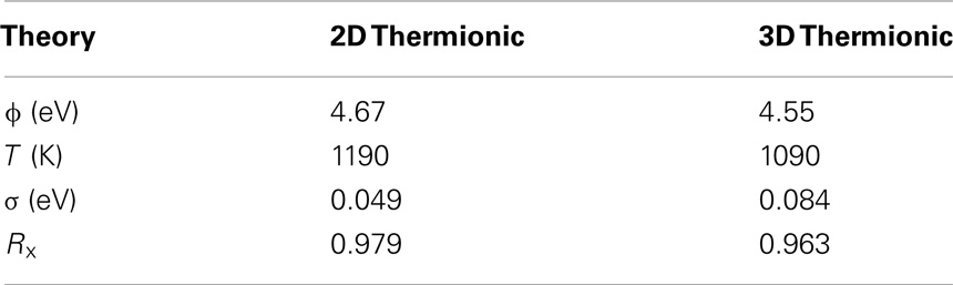
Table 1. Results from data fitting of thermionic theory to an experimental TEED from graphitic petals at a temperature of 1123 K.
The energy at peak intensity and FWHM of the TEEDs for two-dimensional and three-dimensional theory are derived in order to better understand the left-side plot of Figure 7. The energy at peak intensity is found by first solving:
where the Fermi–Dirac statistics describing electron distribution is replaced by Maxwell–Boltzmann statistics.
Once the energy at peak intensity is known, the peak intensity is calculated along with the energies associated with half the peak intensity, allowing for direct calculation of the FWHM. Utilizing this method, the energies at peak intensity for three-dimensional and two-dimensional thermionic theory are EMax3D = EF + ϕ + kB T and EMax2D = EF + ϕ + 1/2 kB T. The corresponding FWHMs are FWHM3D = 2.45 kB T and FWHM2D = 1.80 kB T. These effects are demonstrated in Figure 7. Two-dimensional theory provides less error than three-dimensional theory when data fitting, though neither fit matches exactly to the thermocouple temperature of 1123 K.
Modern Developments of Electron Emission for Energy Conversion
Having established a theoretical basis for thermionic and photo-excited electron emission, we now turn attention to practical functions enabled by such processes. Applications of electron emission have often been motivated by power generation applications and, to a lesser extent, refrigeration (Westover, 2008). One of the first early twentieth century thermionic energy-conversion studies, beyond the work previously discussed on cathode ray tubes, was published by Schlichter (1915) on the conversion of heat into electricity that described the energy exchange between a hot emitter and cold collector. In the study, he analogizes the process to that of fluid evaporation, a comparison often made today for thermionic energy converters. In the second half of the twentieth century, Hatsopoulos (Hatsopoulos and Gyftopoulos, 1973) conducted extensive studies of thermionic energy-conversion devices, performing research in the field over several decades, and publishing a book on the topic in 1973. He spent many years developing thermoelectron engines, consistently improving thermal efficiencies of the devices dating back from early work on a diode configuration in 1958 (Hatsopoulos and Kaye, 1958). Figure 8 contains a schematic of a simple thermionic energy converter, with electron potential, originally presented by Angrist (1976). A very appealing aspect of the energy-conversion device is its simplicity, as the device is driven by a hot emitter separated by vacuum from a cold collector.
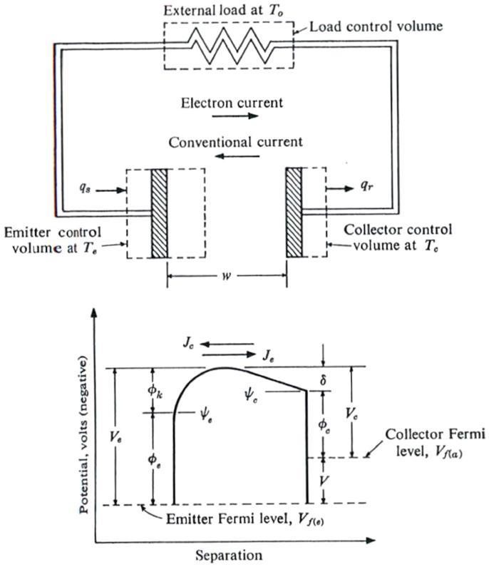
Figure 8. A simple thermionic energy converter schematic (top) and electron potential (bottom). Reprinted with permission from Angrist (1976).
Modified Thermionic Converters
Recent advances in thermionic converters have derived from improvements on the classical metal electrode to exploit the electrode surfaces of thermionic generators. For example, El-Genk and Momozaki (2002) proved for low-temperature applications (<1800 K) that planar molybdenum electrodes with cesium vapor could produce as much as a 70% increase in power density relative to traditional tungsten electrodes with cesium vapor. Furthermore, El-Genk and Luke (1999) demonstrated increases in power output of a simple thermionic converter with macro-grooved molybdenum electrodes relative to smooth electrodes. The simple concept and design provided a directly proportional rise in power output with increased surface area, i.e., a 40% increase in surface area generated a 40% increase in power output.
Thermionic and photo-emission energy converters were often projected for use in extraterrestrial applications, as a high-intensity solar flux is available in space, and maintaining vacuum requires less infrastructure. In space, thermal waste can often be difficult to remove; consequently, utilizing the waste heat in thermionic emission applications is a logical approach. One example of a modified thermionic converter utilized in extraterrestrial applications is an alkali metal thermal to electric converter (AMTEC) (VanHagan et al., 1996), in which the temperature difference between hot and cold electrodes drives a liquid alkali metal “circuit.” Figure 9 provides a schematic of an AMTEC device with a liquid alkali metal circuit, originally published by Tournier (Tournier and El-Genk, 1999). While most AMTEC devices demonstrated conversion efficiencies less than 15%, Tournier and El-Genk (1999) predicted an efficiency of 22.5% for the schematic shown in Figure 9 using a stainless steel cell and molybdenum hot side structure and rhodium coatings. Similar investigations were undertaken in which concentrated light was utilized for energy-conversion applications, including work by Begg et al. (2002).
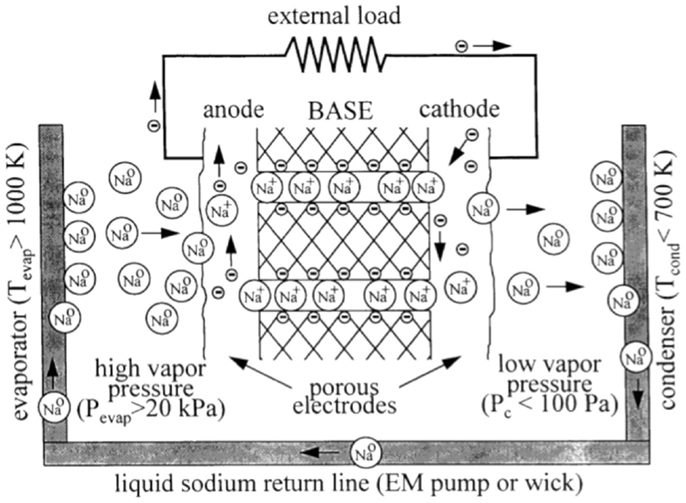
Figure 9. A schematic diagram of sodium AMTEC operating cycle showing microscopic processes. Reprinted with permission from Tournier and El-Genk (1999).
More recently, Jensen (Jensen et al., 2006a,b; Hawkes and Jensen, 2007; Jensen, 2007a,b) and Nemanich (Garguilo et al., 2005; Sun et al., 2011; Koeck and Nemanich, 2012) have produced studies on electron emission with applications in power generation. Combinations of multiple forms of electron emission may offer the most efficient form of energy-conversion moving forward. Jensen et al. (Jensen et al., 2006b; Jensen, 2007b) and Nemanich et al. (Garguilo et al., 2005; Sun et al., 2011) have developed conversion devices utilizing various combinations of thermionic, field, and photoemission.
Photon-Enhanced Thermionic Emission
Some of the most compelling work related to electron emission for energy generation comes from Schwede et al. (2010, 2013) and the PETE concept. PETE combines photovoltaic based photoemission and thermionic emission processes allowing for conversion of photon energy directly to emitted electron energy, while simultaneously utilizing thermalization and photon absorption losses to drive thermionic emission from electrons excited into the emitter band gap. PETE is designed with a structure similar to thermionic converters in which two parallel-plates are separated by a vacuum gap, except that the typically metallic emitter is replaced with a p-type semiconductor. A three-step energy-conversion process takes place. First, electrons are excited by solar irradiation into the conduction band. Second, the electrons rapidly thermalize in the conduction band based on the equilibrium thermal distribution at the emitter’s temperature. Lastly, electrons with energies greater than the electron affinity directly emit to vacuum and are harvested by the collector. Figure 10 provides an energy diagram and schematic for a potential PETE conversion device originally proposed by Schwede et al. (2010).
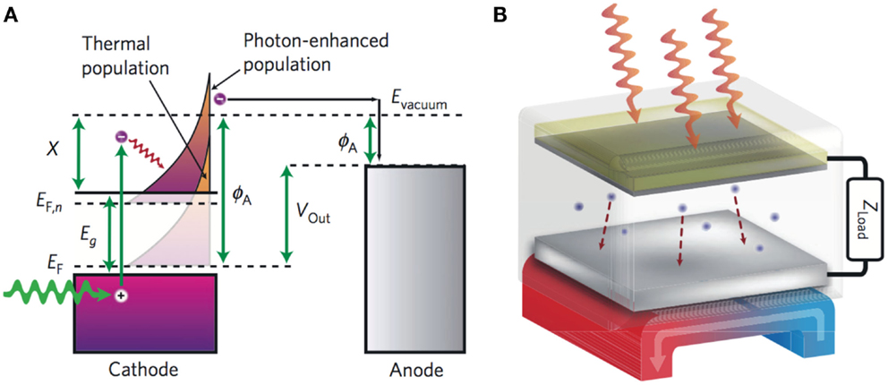
Figure 10. (A) Energy diagram of the PETE process. (B) A schematic of a possible parallel-plate PETE converter. Reprinted with permission from Schwede et al. (2010).
Given that PETE occurs by electrons directly emitted to vacuum after photon absorption, high efficiencies of photovoltaic cells are expected. Schwede demonstrated that increased power conversion efficiency is possible within solar concentrator systems for which large increases in temperature of the emitter are advantageous to electron emission. The PETE concept has led to other theoretical studies modeling the electron-emission process and energy generation, all of which have demonstrated impressive possibilities for PETE applications (Sahasrabuddhe et al., 2012; Varpula and Prunnila, 2012; Segev et al., 2013). For example, Segev et al. (2013) postulated a side-illuminated series of PETE devices with thermal cycle coupling that could generate conversion efficiencies greater than 50%. However, devices of this efficiency have yet to be proven experimentally.
Nanoscale Materials, Structures, and Applications
Limitations in the conversion efficiency of emitter devices have motivated the fabrication of nanostructures that can increase surface area to volume ratios and confine electrons, forcing them to higher energy levels and thereby reducing work functions. For example, Huang et al. (1995) provided theoretical studies on atomically sharp silicon and demonstrated that the local density of states changes dramatically at the emitter tip. Tavkhelidze et al. (2006) demonstrated experimentally that quantum interferences occur in solids with nanoscale features. These quantum interfaces in turn led to reductions in emitter work functions, and with optimized materials, i.e., single crystalline, they anticipate dramatic increases in the quantum interference effects leading to further reductions in work function.
Carbon nanostructures
Carbon nanomaterials exhibit many excellent thermal, optical, and mechanical properties including but not limited to thermal stability and high optical absorption, making them good candidates for thermionic, and photo-emission processes (Avouris et al., 2008; Yang et al., 2008; Westover et al., 2010). Graphitic diamond films (Garguilo et al., 2005; Robinson et al., 2006), carbon nanofibers (Weng et al., 2004), carbon nanowalls (Wu et al., 2004), and carbon nanotubes (CNTs) (Deheer et al., 1995; Saito and Uemura, 2000; Liu et al., 2006) have been studied extensively and exhibit large field enhancement due to low-dimensional features. Nano-crystalline diamond films have provided potential advancements in emitter capabilities in the form of surface coatings, such as hydrogen-terminated layers developed by Robinson et al. (2006) and nitrogen-doped diamond films developed by Sun et al. (2011). While Robinson established that nano-crystalline diamond films could be re-hydrogenated after hydrogen desorption from the surface, only slight reductions in work function were observed with the surface coating and instabilities in the surface coatings took place near 700°C. Nemanich et al. provided some intriguing research related to graphitic diamond films (Garguilo et al., 2005; Sun et al., 2011; Koeck and Nemanich, 2012), as well as work regarding negative-electron-affinity of diamond films (Vanderweide et al., 1994). Research by Weng et al. (2004) determined that vertically aligned carbon nanofibers exhibit a high current density via field emission that can be further enhanced by treatment within argon plasma. Variations of carbon nanowalls (graphitic nanopetals) are discussed in great detail elsewhere (McCarthy et al., 2013) and throughout this report, but the interested reader should refer to Wu’s review (Wu et al., 2004) of carbon nanowalls, and other similar materials, which discusses at length the growth mechanisms and resulting properties of this two-dimensional material.
CNTs have exhibited unique optical properties. Yang et al. (2008) developed CNTs engineered to have near-perfect optical absorption, and Avouris et al. (2008) demonstrated an ability to ‘tune’ the direct-bandgap of semiconducting CNTs based on their diameter. CNTs also have great potential for thermionic and field-emission applications. Deheer et al. (1995) fabricated a high-intensity electron gun from multi-walled CNTs for flat panel display applications. Similarly, Saito (Saito and Uemura, 2000) fabricated CNT arrays capable of ultra-high luminescence with applications in cathode ray tubes and vacuum fluorescence displays. Figure 11 contains a schematic of a thermionic energy converter with carbon-nanotube yarn as the emitter, originally published by Liu et al. (2006). Liu et al. researched thermionic emission from multi-walled CNT yarns and showed larger emission constants relative to conventional thermionic cathodes. While reductions in work function of the yarns were not demonstrated relative to bulk graphite, the increased emission constant may result from a very high surface area that arises from the nanoscale, composite material.
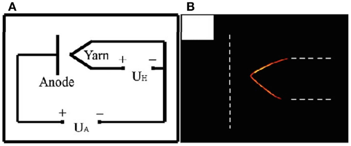
Figure 11. (A) Electrical circuit of thermionic energy converter with CNT yarn. (B) Optical image of CNT yarn heated to 1333 K by a DC current. Reprinted with permission from Liu et al. (2006).
Graphene has been of particular interest in recent investigations (Palnitkar et al., 2010), including single-layer graphene (Xiao et al., 2010), few-layer graphene (Wang et al., 2006), and graphene polymers (Eda et al., 2008; Wu et al., 2009). Palnitkar et al. (2010) showed remarkably low turn-on voltage (<1 V/μm) for doped and undoped graphene while Xiao et al. (2010) presented theoretical results suggesting that even lower turn-on voltages and higher current densities are possible for single-layer graphene. Multi-layer graphene has been developed experimentally in a packaged field-emission device by Wang et al. (2006) and has exhibited large emission currents, though at larger turn-on voltages than few or single-layer graphene (<10 V/μm). While few to single-layer graphene holds great promise for electron-emission applications, difficulties in fabricating, and packaging the material may limit their implementation. Graphene-polymer composites offer a cheaper alternative to pure graphene that is much simpler to fabricate. Furthermore, Eda et al. (2008) and Wu et al. (2009) demonstrated that simple graphene-polymer composite films are still capable of large field-emission current with low-turn-on voltages (<10 V/μm).
Graphitic petals grown from graphitic substrates offer an intriguing material for electron-emission applications. Bhuvana et al. (2010) first demonstrated the fabrication of graphitic petals by plasma enhanced chemical vapor deposition. The petals have many sharp edges and a high surface area to volume ratio creating a material that is favorable for electron emission (McCarthy et al., 2013). In addition to many excellent material properties, the atomic structure of graphite and few-layer graphene offers the opportunity for intercalation of the lattice with alkali metals. Utilization of alkali metals with electron-emission driven energy converters has been practiced extensively in the past with perhaps the most classical approach being cesium coated thermionic and field emitting converters (Paramonov and ElGenk, 1997). Similarly, Osterlund et al. (1999) demonstrated experimentally that a single monolayer of potassium adsorped on graphite decreases the work function to that of potassium (2.3 eV). Davydov (2009) has further reinforced this result theoretically.
Dresselhaus and Dresselhaus (2002) wrote an exhaustive study on the intercalation compounds of graphite including but not limited to lithium and potassium intercalation. Very interesting electrical properties result from “doping” graphitic materials with these alkali metals. Previous work has demonstrated that carbon nanofibers (Robinson et al., 2005), nanotubes (Westover et al., 2010), and graphitic petals (McCarthy et al., 2013) intercalated with potassium have excellent thermionic and photo-emission trends and are relatively stable to high temperatures. For example, Westover et al. (2010) and Robinson et al. (2005) have both demonstrated reductions in the work function of potassium-intercalated CNTs and graphitic nanofibers, respectively.
Electron-emission refrigeration
Electron emission as a means of refrigeration is a specialized field that typically requires field emission. Though prior works suggests the possibility for refrigeration derived from electron emission, a viable device has yet to be developed. However, nanoscale materials may offer an avenue for generating a commercially viable, room-temperature refrigeration device driven by electron emission.
Theory explaining this form of refrigeration is derived from the Nottingham effect describing energy-exchange attending field emission. Fleming (Fleming and Henderson, 1940) and Nottingham (1941) provided experimental and theoretical results indicating that low-temperature field-emission produced negligible energy losses during electron exchange, but higher temperatures in which thermionic emission was prominent led to increased heating of the emitter as electrons no longer tunneled through the surface barrier efficiently. Bergeret et al. (1985) showed that Nottingham heating can occur in a ultra-low temperature (<5 K), sharp superconducting tips (niobium) under high electric fields (>3 × 10⁷ V/cm). More recently, Xu et al. (1994) noted that there are two main modes of heating during field-emission, both dependent on the current, I. The first mode of heating is resistive heating (~I2) and the second mode results of Nottingham heating (~I). For cold temperatures and low current densities, Nottingham heating is the dominant contributor to heat accumulation within the emitter, while high-temperatures and high current densities lead to increases in resistive heating.
While early reports of the Nottingham effect only presented heating of emitters, both heating and cooling due to electron emission can be described by the Nottingham effect. Swanson et al. (1966) observed a transition from emitter heating to emitter cooling take place but at a high transition temperature of approximately 500 K. More recently, Hishinuma et al. (2003) reported a cooling effect of 1–10 nW produced by thermionic emission across nanometer gaps at RT. Figure 12 contains a plot of experimentally derived energy exchange at an emitter tip reported by Swanson et al. (1966). At elevated temperatures (>500 K), cooling occurred at the emitter for low field-emission currents where the net energy exchange was negative. For a high work function material, such as the tungsten tip utilized by Swanson, net cooling was only on the order of 1 μW.
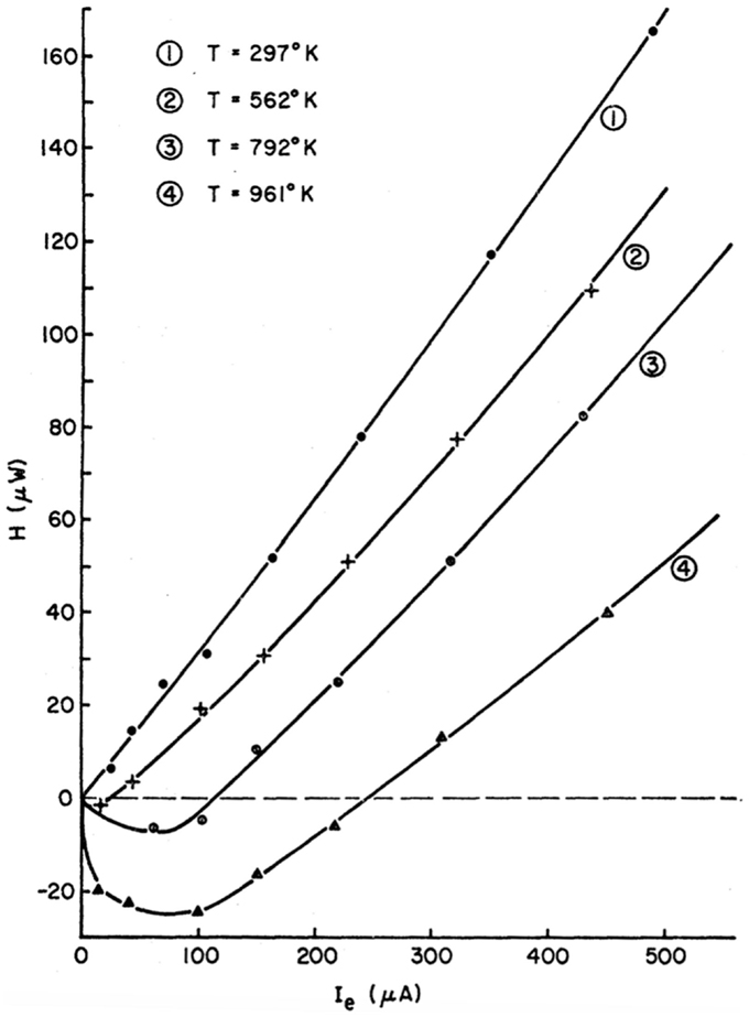
Figure 12. Net energy exchange H leaving a tungsten tip at a variety of temperatures as a function of field-emission current. Reprinted with permission from Swanson et al. (1966).
Moving forward, nanoscale geometries may offer a promising means of generating emitter cooling, as confinement effects will create a preference toward high-energy electron emission, and reductions in work function could lead to exponential increases in net energy exchange resulting in substantial cooling. Fisher and Walker (2002) have presented theoretical studies indicating that arrays of nanoscale emitters with sharp tips and low work functions have the potential to produce large cooling fluxes (~W/m2 for ϕ = 1.0 eV and tip radius <25 nm).
Conclusion
This review has provided an overview of thermally and photonically driven electron emission, including some of the century-old seminal studies as well as issues associated with modern nanomaterials. The theoretical underpinnings of these photo-emission processes, culminating in combined effects, presented primarily in a Landauer formulation provide a common basis for analysis and interpretation of experimental results that can derive from a complicated interplay involving broad-band (e.g., solar) excitation sources, internal scattering mechanisms, and low-dimensional effects associated with nanoscale emitters. The hope is that the collection of this information in one source will assist future researchers in developing new insights into coupled mechanisms to enhance electron emission and new understanding of experimental results.
Even though electron emission as a subject of scientific research is almost ancient by modern research standards, it has not produced transformative changes in energy-conversion technology. Recent advances in the ability to control (and to a lesser extent mass-produce) nanomaterials elicits some hope that such major breakthroughs are possible. PETE technology, for example, offers a theoretical basis for energy generation at practically relevant efficiencies and capacities, but related issues of electron yield and the generation of a suitable quasi-equilibrium state remain to be understood further and then optimized. Direct refrigeration by electron emission has been known to be possible at elevated temperatures, but its realization in practical capacities at or near RT will require new discoveries in materials, surface science, and likely device structures. As demonstrated with work by Schwede et al. (2010) and Fisher (Fisher and Walker, 2002), successful development of high-efficiency, cost-effective electrical power generation will likely depend on advances in semiconductor technology, and on large-scale manufacturing of nanoscale materials. An experimentally verified PETE device would demonstrate a significant breakthrough in electron-emission-driven energy generation devices. Similarly, the ability to generate nanoscale emitter tips consistently over large areas could provide significant advancements in refrigeration by electron emission and energy-conversion applications via field emission and combinations of field, thermionic, and photoemission. Lastly, advances in the fields of photovoltaics and field emission may continue to present new avenues for thermionic and photo-emission research, such as the way that an ideal PETE device has been hypothesized. Our belief is that the simplicity of operation of electron-emission devices and the possibility that practically relevant efficiencies are possible combine to merit continued and increased scientific research.
Conflict of Interest Statement
Timothy S. Fisher hereby informs the journal of his position as Founder and Chief Technology Officer of BlueVine Graphene Industries, Inc., a company whose business activities include the development of supercapacitors and biosensors. The submitted work is an academic study and is not intended or represented as a commercial product or promotion. The other co-authors declare that the research was conducted in the absence of any commercial or financial relationships that could be construed as a potential conflict of interest.
Acknowledgments
This work was supported by the Ingersoll-Rand fellowship provided through the School of Mechanical Engineering, Purdue University. The authors would like to thank Tianyin Sun and Robert Nemanich for their assistance with implementing scattering effects into the REM.
References
Angrist, S. W. (1976). “Direct energy conversion,” in Allyn and Bacon Series in Mechanical Engineering and Applied Mechanics, 3rd Edn (Boston: Allyn and Bacon), 233–278.
Avouris, P., Freitag, M., and Perebeinos, V. (2008). Carbon-nanotube photonics and optoelectronics. Nat. Photonics 2, 341–350. doi:10.1038/nphoton.2008.94
Becquerel, M. E. (1853). Researches on the electrical conductivity of gases at high temperatures. Philos. Mag. Ser. 4, 456–457.
Begg, L. L., Streckert, H. S., Peltier, D., and Watson, J. (2002). Conceptual design of high power advanced low mass (HPALM) solar thermionic power system. 2002 37th Intersociety Energy Conversion Engineering Conference (IECEC), Washington, DC.
Bergeret, H., Septier, A., and Drechsler, M. (1985). Nottingham effect of a superconducting metal. Phys. Rev. B 31, 149–153. doi:10.1103/PhysRevB.31.149
Berglund, C. N., and Spicer, W. E. (1964a). Photoemission studies of copper and silver: experiment. Phys. Rev. A Gen. Phys. 136, 1044. doi:10.1103/PhysRev.136.A1044
Berglund, C. N., and Spicer, W. E. (1964b). Photoemission studies of copper and silver: Theory. Phys. Rev. A Gen. Phys. 136, 1044. doi:10.1103/PhysRev.136.A1044
Bhuvana, T., Kumar, A., Sood, A., Gerzeski, R. H., Hu, J., Bhadram, V. S., et al. (2010). Contiguous petal-like carbon nanosheet outgrowths from graphite fibers by plasma CVD. ACS Appl. Mater. Interfaces 2, 644–648. doi:10.1021/am9009154
Davydov, S. Y. (2009). Adsorption of potassium on graphite: work function calculations. Tech. Phys. Lett. 35, 847–849. doi:10.1134/S1063785009110078
Deheer, W. A., Chatelain, A., and Ugarte, D. (1995). A carbon nanotube field-emission electron source. Science 270, 1179–1180. doi:10.1126/science.270.5239.1179
Dresselhaus, M. S., and Dresselhaus, G. (2002). Intercalation compounds of graphite. Adv. Phys. 51, 1–186. doi:10.1080/00018730110113644
DuBridge, L. A. (1933). Theory of the energy distribution of photoelectrons. Phys. Rev. 43, 0727–0741. doi:10.1103/PhysRev.43.727
Eda, G. H., Unalan, E., Rupesinghe, N., Amaratunga, G. A. J., and Chhowalla, M. (2008). Field emission from graphene based composite thin films. Appl. Phys. Lett. 93, 233502. doi:10.1063/1.3028339
El-Genk, M. S., and Luke, J. R. (1999). Performance comparison of thermionic converters with smooth and macro-grooved electrodes. Energy Convers. Manag. 40, 319–334. doi:10.1016/S0196-8904(98)00049-1
El-Genk, M. S., and Momozaki, Y. (2002). An experimental investigation of the performance of a thermionic converter with planar molybdenum electrodes for low temperature applications. Energy Convers. Manag. 43, 911–936. doi:10.1016/S0196-8904(01)00084-X
Fisher, T. (2013). “Thermal Energy at the Nanoscale,” in Lessons From Nanoscience: A Lecture Note Series, ed. World Scientific Book (Hackensack, NJ), 1–166.
Fisher, T. S., and Walker, D. G. (2002). Thermal and electrical energy transport and conversion in nanoscale electron field emission processes. J. Heat Transfer Trans. ASME 124. doi:10.1115/1.1494091
Fleming, G. M., and Henderson, J. E. (1940). The energy losses attending field current and thermionic emission of electrons from metals. Phys. Rev. 58, 887–894. doi:10.1103/PhysRev.58.887
Fowler, R. H. (1931). The analysis of photoelectric sensitivity curves for clean metals at various temperatures. Phys. Rev. 38, 45–56. doi:10.1103/PhysRev.38.45
Fowler, R. H., and Nordheim, L. (1928). Electron emission in intense electric fields. Proc. R Soc. Lond. A 119, 173–181. doi:10.1098/rspa.1928.0091
Gadzuk, J. W., and Plummer, E. W. (1973). Field-emission energy-distribution (FEED). Rev. Mod. Phys. 45, 487–548. doi:10.1103/RevModPhys.45.487
Garguilo, J. M., Koeck, F. A. M., Nemanich, R. J., Xiao, X. C., Carlisle, J. A., and Auciello, O. (2005). Thermionic field emission from nanocrystalline diamond-coated silicon tip arrays. Phys. Rev. B 72. doi:10.1103/PhysRevB.72.165404
Good, R. H., and Muller, E. W. (1956). “Field Emission,” in Electron-Emission Gas Discharges. ed. S. Flugge (Berlin: Springer Berlin Heidelberg), 176–231.
Guthrie, F. (1873). On a relation between heat and static electricity. Philos. Mag. Ser. 4, 257–266.
Hatsopoulos, G. N., and Gyftopoulos, E. P. (1973). Thermionic Energy Conversion, Vol. 2. Cambridge: MIT Press.
Hatsopoulos, G. N., and Kaye, J. (1958). Analysis and experimental results of a diode configuration of a novel thermoelectron engine. Proc. Inst. Radio Eng. 46, 574–579.
Hawkes, P. W., and Jensen, K. L. (2007). “Electron emission physics,” in Electron Emission Physics (San Diego, CA: Academic Press), 4–306.
Hertz, H. (1893). Electric Waves; Being Researches on the Propagation of Electric Action with Finite Velocity Through Space. (New York, NY: Macmillan and Company), 1–268.
Hishinuma, Y., Geballe, T. H., Moyzhes, B. Y., and Kenny, T. W. (2003). Measurements of cooling by room-temperature thermionic emission across a nanometer gap. J. Appl. Phys. 94, 4690–4696. doi:10.1063/1.1606852
Huang, Z. H., Cutler, P. H., Miskovsky, N. M., and Sullivan, T. E. (1995). Calculation of local-density of states at an atomically sharp Si tip. J. Vacuum Sci. Technol. B 13, 522–525. doi:10.1116/1.588346
Jensen, K. L. (2007a). “Electron Emission Physics,” in Advances in Imaging and Electron Physics, ed. L. J. Kevin (San Diego, CA: Elsevier), 147–279.
Jensen, K. L. (2007b). General formulation of thermal, field, and photoinduced electron emission. J. Appl. Phys. 102, 024911. doi:10.1063/1.2786028
Jensen, K. L., Feldman, D. W., Moody, N. A., and O’Shea, P. G. (2006a). A photoemission model for low work function coated metal surfaces and its experimental validation. J. Appl. Phys. 99, 124905. doi:10.1063/1.2203720
Jensen, K. L., Feldman, D. W., Moody, N. A., and O’Shea, P. G. (2006b). Field-enhanced photoemission from metals and coated materials. J. Vacuum Sci. Technol. B 24, 863–868. doi:10.1116/1.2183780
Koeck, F. A. M., and Nemanich, R. J. (2012). Substrate-diamond interface considerations for enhanced thermionic electron emission from nitrogen doped diamond films. J. Appl. Phys. 112, 113707. doi:10.1063/1.4766442
Liu, P., Wei, Y., Jiang, K. L., Sun, Q., Zhang, X. B., Fan, S. S., et al. (2006). Thermionic emission and work function of multiwalled carbon nanotube yarns. Phys Rev B 73, 235412. doi:10.1103/PhysRevB.73.235412
MATLAB, 2011b. (2011). MathWorks Announces Release 2011b of the MATLAB and Simulink Product Families. Natick, MA: The Mathworks Inc.
McCarthy, P. (2013). Thermal Energy Harvesting and Solar Energy Conversion Utilizing Carbon-Based Nanomaterials. Ph.D., Mechanical Engineering, Purdue University.
McCarthy, P., Laan, S. V., Janes, D., and Fisher, T. (2013). Photonically excited electron emission from modified graphitic nanopetal arrays. J. Appl. Phys. 113, 193710. doi:10.1063/1.4805038
McMullen, K. J. (2010). Measurement of Thermionic Electron Emission from Modified Graphene Petals. West Lafayette, IN: MSME, Mechanical Engineering, Purdue University.
Murphy, E. L., and Good, R. H. (1956). Thermionic emission, field emission, and the transition region. Phys. Rev. 102, 1464–1473. doi:10.1103/PhysRev.102.1464
Nottingham, W. B. (1941). Remarks on energy losses attending thermionic emission of electrons from metals. Phys. Rev. 59, 906–907. doi:10.1103/PhysRev.59.906.2
Osterlund, L., Chakarov, D. V., and Kasemo, B. (1999). Potassium adsorption on graphite(0001). Surf. Sci. 420, 174–189. doi:10.1016/S0039-6028(98)00822-X
Palnitkar, U. A., Kashid, R. V., More, M. A., Joag, D. S., Panchakarla, L. S., and Rao, C. N. R. (2010). Remarkably low turn-on field emission in undoped, nitrogen-doped, and boron-doped graphene. Appl. Phys. Lett. 97, 063102. doi:10.1063/1.3464168
Paramonov, D. V., and ElGenk, M. S. (1997). A review of cesium thermionic converters with developed emitter surfaces. Energy Convers. Manag. 38, 533–549. doi:10.1016/S0196-8904(96)00067-2
Reifenberger, R., Goldberg, H. A., and Lee, M. J. G. (1979). Measurement of the total energy-distribution in photoinduced field-emission. Surf. Sci. 83, 599–616. doi:10.1016/0039-6028(79)90066-9
Robinson, V. S., Fisher, T. S., Michel, J. A., and Lukehart, C. M. (2005). Work function reduction of graphitic nanofibers by potassium intercalation. Appl. Phys. Lett. 87, 113707. doi:10.1063/1.2009052
Robinson, V. S., Show, Y., Swain, G. M., Reifenberger, R. G., and Fisher, T. S. (2006). Thermionic emission from surface-terminated nanocrystalline diamond. Diamond Relat. Mater. 15, 1601–1608. doi:10.1016/j.diamond.2006.01.017
Sahasrabuddhe, K., Schwede, J. W., Bargatin, I., Jean, J., Howe, R. T., Shen, Z.-X., et al. (2012). A model for emission yield from planar photocathodes based on photon-enhanced thermionic emission or negative-electron-affinity photoemission. J. Appl. Phys. 112, 094907. doi:10.1063/1.4764106
Saito, Y., and Uemura, S. (2000). Field emission from carbon nanotubes and its application to electron sources. Carbon N. Y. 38, 169–182. doi:10.1016/S0008-6223(99)00139-6
Schlichter, W. (1915). Spontaneous electron emission from glowing metals and thermo-electric elements. Ann. Phys. 47, 573–640. doi:10.1002/andp.19153521302
Schwede, J. W., Bargatin, I., Riley, D. C., Hardin, B. E., Rosenthal, S. J., Sun, Y., et al. (2010). Photon-enhanced thermionic emission for solar concentrator systems. Nat. Mater. 9, 762–767. doi:10.1038/nmat2814
Pubmed Abstract | Pubmed Full Text | CrossRef Full Text | Google Scholar
Schwede, J. W., Sarmiento, T., Narasimhan, V. K., Rosenthal, S. J., Riley, D. C., Schmitt, F., et al. (2013). Photon-enhanced thermionic emission from heterostructures with low interface recombination. Nat. Commun. 4, 1576–1576. doi:10.1038/ncomms2577
Pubmed Abstract | Pubmed Full Text | CrossRef Full Text | Google Scholar
Segev, G., Kribus, A., and Rosenwaks, Y. (2013). High performance isothermal photo-thermionic solar converters. Solar Energy Mater. Solar Cells 113, 114–123. doi:10.1016/j.solmat.2013.02.002
Spicer, W. E., and Herreragomez, A. (1993). Modern theory and applications of photocathodes. 1st Conference on Photodetectors and Power Meters, San Diego, CA.
Sun, T., Franz, A. M., Zhu, K. C., and Nemanich, R. J. (2011). Combined visible light photo-emission and low temperature thermionic emission from nitrogen doped diamond films. Appl. Phys. Lett. 99, 202101. doi:10.1063/1.3658638
Swanson, L. W., Crouser, L. C., and Charbonnier, F. M. (1966). Energy exchanges attending field electron emission. Phys. Rev. 151, 327. doi:10.1103/PhysRev.151.327
Tavkhelidze, A., Bibilashvili, A., Jangidze, L., Shimkunas, A., Mauger, P., Rempfer, G. F., et al. (2006). Observation of quantum interference effect in solids. J. Vacuum Sci. Technol. B 24, 1413–1416. doi:10.1116/1.2198856
Tournier, J. M., and El-Genk, M. S. (1999). Performance analysis of Pluto/Express, multitube AMTEC cells. Energy Convers. Manag. 40, 139–173. doi:10.1016/S0196-8904(98)00048-X
Vander Laan, S. J. (2011). Photonically and Thermally Excited Electron Emission from Modified Graphitic Nanopetals. West Lafayette, IN: MSECE, Purdue University.
Vanderweide, J., Zhang, Z., Baumann, P. K., Wensell, M. G., Bernholc, J., and Nemanich, R. J. (1994). Negative-electron-affinity effects on the diamond (100) surface. Phys Rev B 50, 5803–5806. doi:10.1103/PhysRevB.50.5803
VanHagan, T. H., Smith, J. N., and Schuller, M. (1996). Thermionic/AMTEC cascade converter concept for high-efficiency space power. 31st Intersociety Energy Conversion Engineering Conference (IECEC 96), Washington, DC.
Varpula, A., and Prunnila, M. (2012). Diffusion-emission theory of photon enhanced thermionic emission solar energy harvesters. J. Appl. Phys. 112, 044506. doi:10.1063/1.4747905
Wang, S., Wang, J., Miraldo, P., Zhu, M., Outlaw, R., Hou, K., et al. (2006). High field emission reproducibility and stability of carbon nanosheets and nanosheet-based backgated triode emission devices. Appl. Phys. Lett. 89, 183103. doi:10.1063/1.2372708
Weng, C. H., Leou, K. C., Wei, H. W., Juang, Z. Y., Wei, M. T., Tung, C. H., et al. (2004). Structural transformation and field emission enhancement of carbon nanofibers by energetic argon plasma post-treatment. Appl. Phys. Lett. 85, 4732–4734. doi:10.1063/1.1815062
Westover, T. L., Franklin, A. D., Cola, B. A., Fisher, T. S., and Reifenberger, R. G. (2010). Photo- and thermionic emission from potassium-intercalated carbon nanotube arrays. J. Vacuum Sci. Technol. B 28, 423–434. doi:10.1116/1.3368466
Westover, T. L. (2008). Energy Transport and Conversion in Electron Emission Processes. Ph.D., Purdue University.
Wu, Y. H., Yang, B. J., Zong, B. Y., Sun, H., Shen, Z. X., and Feng, Y. P. (2004). Carbon nanowalls and related materials. J. Mater. Chem. 14, 469–477. doi:10.1039/b311682d
Wu, Z.-S., Pei, S., Ren, W., Tang, D., Gao, L., Liu, B., et al. (2009). Field emission of single-layer graphene films prepared by electrophoretic deposition. Adv. Mater. Weinheim 21, 1756. doi:10.1002/adma.200802560
Xiao, Z., She, J., Deng, S., Tang, Z., Li, Z., Lu, J., et al. (2010). Field electron emission characteristics and physical mechanism of individual single-layer graphene. ACS Nano 4, 6332–6336. doi:10.1021/nn101719r
Pubmed Abstract | Pubmed Full Text | CrossRef Full Text | Google Scholar
Xu, J. B., Lauger, K., Moller, R., Dransfeld, K., and Wilson, I. H. (1994). Energy-exchange processes by tunneling electrons. Appl. Phys. A Mater. Sci. Process. 59, 155–161. doi:10.1007/BF00332209
Yang, Z.-P., Ci, L., Bur, J. A., Lin, S.-Y., and Ajayan, P. M. (2008). Experimental observation of an extremely dark material made by a low-density nanotube array. Nano Lett. 8, 446–451. doi:10.1021/nl072369t
Pubmed Abstract | Pubmed Full Text | CrossRef Full Text | Google Scholar
Keywords: thermionic, electron emission, photoemission, photo-emission spectroscopy, graphene
Citation: McCarthy PT, Reifenberger RG and Fisher TS (2014) Thermionic and photo-excited electron emission for energy-conversion processes. Front. Energy Res. 2:54. doi: 10.3389/fenrg.2014.00054
Received: 09 September 2014; Paper pending published: 12 October 2014;
Accepted: 09 November 2014; Published online: 09 December 2014.
Edited by:
Uros Cvelbar, Jozef Stefan Institute, SloveniaCopyright: © 2014 McCarthy, Reifenberger and Fisher. This is an open-access article distributed under the terms of the Creative Commons Attribution License (CC BY). The use, distribution or reproduction in other forums is permitted, provided the original author(s) or licensor are credited and that the original publication in this journal is cited, in accordance with accepted academic practice. No use, distribution or reproduction is permitted which does not comply with these terms.
*Correspondence: Timothy S. Fisher, Birck Nanotechnology Center, 1205 West State Street, West Lafayette, IN 47907, USA e-mail: tsfisher@purdue.edu