Ordered nanomaterial thin films via supported anodized alumina templates
 Mohammed Es-Souni*
  Salah Habouti
- Institute for Materials and Surface Technology, University of Applied Sciences, Kiel, Germany
Supported anodized alumina template films with highly ordered porosity are best suited for fabricating large-area ordered nanostructures with tunable dimensions and aspect ratios. In this paper, we first discuss important issues for the generation of such templates, including required properties of the Al/Ti/Au/Ti thin-film heterostructure on a substrate for high-quality templates. We then show examples of anisotropic nanostructure films consisting of noble metals using these templates, discuss briefly their optical properties and their applications to molecular detection using surface-enhanced Raman spectroscopy. Finally, we briefly address the possibility to make nanocomposite films, exemplary shown on a plasmonic–thermochromic nanocomposite of VO2-capped Au-nanorods.
Introduction
Ordered nanomaterial’s thin films may be processed using a variety of methods, among them, electron beam and soft lithography (Xia and Whitesides, 1998; Gates et al., 2005), self-assembly (Grzelczak et al., 2010) or a combination of both (Yan et al., 2009), and solid templates, e.g., see review by Jones et al. (2011). Glancing angle deposition techniques, a modification to physical vapor deposition, were also advantageously used to fabricate ordered nanomaterial’s films either on bare or pre-patterned surfaces, although in most of the cases, oblique nanostructures with limited control of periodicity are obtained with this method (e.g., Gish et al., 2006; Liu et al., 2010; Camelio et al., 2014). While e-beam lithography is a powerful technique for making ordered nanomaterials of almost any shape and gap between nanostructures, the processing cost, including investment and consumables, is high. Self-assembly is a powerful bottom-up technique that has been demonstrated for ordered nanostructures of a variety of materials (Mann, 2009; Grzelczak et al., 2010), but issues of up-scalability are still to be addressed. Another bottom-up technique that is of particular interest relies on solid templates, especially porous anodized alumina (PAA) templates, for making large-area ordered nanomaterials with different aspect ratios and, to some extent, morphology (Hulteen and Martin, 1997; Jones et al., 2011). The technique is straightforward because the porous template molds the deposited material into the predefined pore dimension and periodicity. Moreover, it is cost-effective because of low investment and consumable costs. PAA are known since the pioneering work of Masuda and Fukuda (1995). Using two-step anodization of high purity, well-annealed aluminum sheets, it is possible to process alumina membranes with highly ordered domains. Pore size and periodicity may be tuned via different anodization conditions, including different electrolytes and anodization voltages (e.g., Lee et al., 2006). These membranes may be chemically detached from the parent metal and used, after some necessary processing steps, for fabricating monolithic and composite nanomaterials. Nanostructure synthesis is achieved by filling the pore channels either by soaking the membrane in appropriate precursor solutions, by self-assembly or by electrodeposition (Hulteen and Martin, 1997; Jones et al., 2011). The latter is probably best suited for the fabrication of nanowires of various metals (Hulteen and Martin, 1997; Jones et al., 2011). However, main drawbacks are the difficult handling of the free-standing fragile membranes and the many necessary pre-handling steps such as mechanical stabilizing and electroding. Furthermore, exposure of the nanostructures, e.g., for device fabrication, etc. requires dissolving the membrane, which could result in the collapse of high aspect ratio nanostructures and the sticking together of the nanowires to form large bundles. Often characterization of free-standing nanostructure arrays is laborious because the character of the nanostructure is lost and with it also the suitability for such applications as sensing, e.g., optical and nanobiological.
Recently, a new type of template was proposed that consists of thin anodized aluminum films, a few hundreds of nanometers to a few micrometers thick, supported on solid or flexible substrates (Mallet et al., 2005; Piraux et al., 2007; Wurtz et al., 2007; Foong et al., 2008; Mátéfi-Tempfli and Mátéfi-Tempfli, 2009). In general, the aluminum film is deposited on silicon, glass, or indium-thin oxide (ITO) coated glass wafers that have been pre-coated with a thin adhesion layer (a few nanometers) and a gold (a few tens of nanometers) electrode. Anodization, pore opening, and barrier-layer etching are performed in a similar way to bulk aluminum. Supported templates were successfully used in a few reports for the processing of magnetic nano-hetero-structures (Mallet et al., 2005; Piraux et al., 2007; Wurtz et al., 2007), Au-NRs (Wurtz et al., 2007), and Ni-NWs (Foong et al., 2008). In the following, we intend to concentrate on this type of templates because they have promising potential in the processing of large area, wafer size, ordered nanostructure films. We will address the processing strategy and the critical fabrication aspects of PAAF. A few examples of ordered nanostructures that were processed using PAAF as well as their applications are also presented.
Critical Steps in the Fabrication of PAAF
PAAF have been used in a few reports for the processing of anisotropic nanostructures, but their processing steps were not discussed in due details. Herein, we address important requirements for thin-film metal heterostructure for successful anodization.
For the fabrication of PAAF, it is first necessary to process a thin-film heterostructure on a substrate consisting of an adhesion layer, an electrode, and the Al-film to be anodized. The adhesion layer is usually an ultra-thin Ti film of few nanometers (2–5 nm) on top of which an Au-film of 5–20 nm is sputtered to serve as electrode. In order to improve adhesion between Au and the subsequently deposited Al-film, it is advised to use the same Ti adhesion layer. The main advantage of Ti lies in its ability to form strong intermetallic bonds with both metals at the interface [see related phase diagrams (Murray, 1983; Kattner et al., 1992)]. A PVD system that allows deposition of the thin-film heterostructure without breaking the vacuum (in order to prevent oxidation of the reactive metals) is best suited for high-quality PAAF. However, because the Al-film is subjected to high stresses during anodization, the requirements on the Al-film adhesion are high. Further, the formation of well-ordered pore domains is dependent on film microstructure and roughness. Films free of spikes and highly smooth are best suited. The conditions for obtaining these films must be iterated for the particular substrate and PVD system used. Below we summarize our own experience in growing film heterostructures using either sputtering (RF or DC) or e-beam evaporation of Al.
While sputtering of Ti and Au is in principle easily achieved, provided the substrate is clean and the PVD chamber is free from contaminants, there are some critical issues to be dealt with when depositing the Al-film. Sputtering of Al had in our case invariably led to rough films because the sputtering rate of Al was relatively low at the conditions chosen (below 0.16 nm/s at an argon pressure of 10−3 mbar and 220 W; these conditions were iteratively found to yield films with best adhesion properties for successful anodization). Under these conditions, the deposition of the desired 500–600 nm thick films took approximately 1 h, which resulted in substrate heating and grain growth. Even when the films were sputtered with extreme precaution to avoid heating, e.g., sequential sputtering with waiting time for the substrate to cool down, the results remained unsatisfactory. An example is shown in Figure 1.
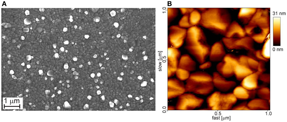
Figure 1. Top views of a sputtered Al-film of 400 nm thickness; sequential sputtering under the conditions described in the main text (see above). (A) SEM micrograph; (B) AFM-amplitude micrograph (1 × 1μm2). The root mean square (rms) roughness of the film is 7.1 nm.
Anodization of such films leads to poor pore ordering and verticality as exemplary, shown in Figure 2.
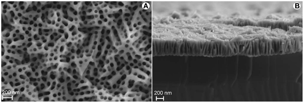
Figure 2. SEM micrographs of PAAF obtained from sputtered Al-films. (A) Top view showing poor pore ordering; (B) cross-section showing poor verticality of the pores. Scale bar 200 nm.
Smoother and more homogeneous Al-films are obtained at high deposition rates by electron beam evaporation while maintaining substrate temperature low. In this process, an applied magnetic field allows dynamically deflecting the electron beam in x–y directions with a given frequency in order to ensure a homogeneous material evaporation, and the substrate is rotated during deposition to achieve uniform material thickness over the whole surface. A PVD system equipped with a module for e-beam evaporation is, therefore, necessary in order to obtain high-quality Al-films. After the sequential sputtering of Ti and Au, Al is e-beam evaporated without breaking the vacuum. The film microstructure obtained is exemplary shown in Figure 3, and the resulting anodized film in Figures 4A,B.
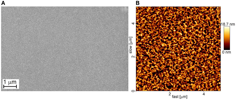
Figure 3. Top views of an Al-film obtained by e-beam evaporation; the film is 600 nm thick (A) SEM and (B) AFM micrographs. The rms roughness of the film is 4.2 nm. The substrate is silicon.
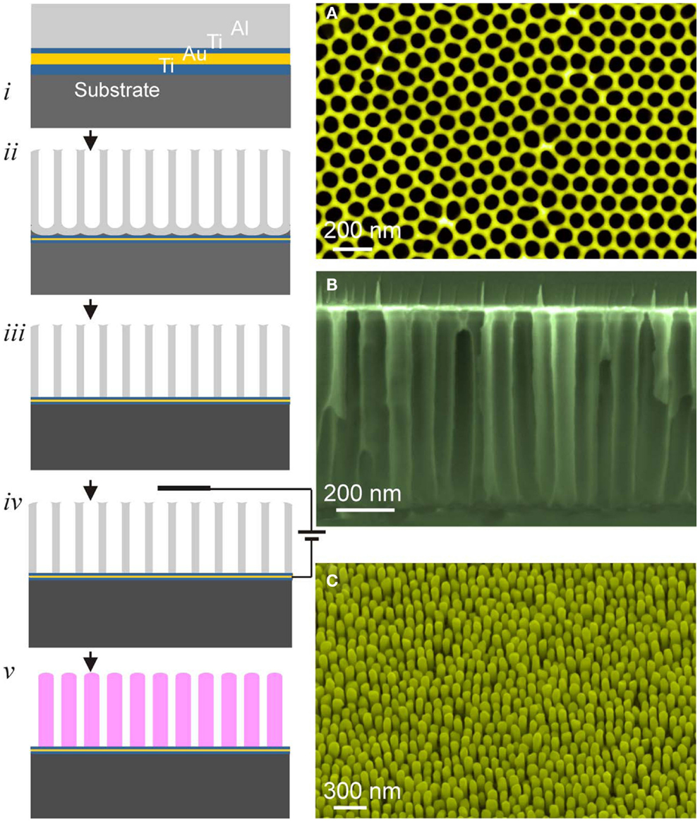
Figure 4. Left: schematic illustration of the processing steps of PAAF: (i) film heterostructure, (ii) anodization, (iii) barrier-layer opening, (iv,v) electrodeposition and PAAF removal, exposing the nanostructure array. Right: (A) top view of a PAAF, (B) cross-section, and (C) on-substrate nanorods (Au-nanorods in this case).
Al-Film Anodization
Once a well-adherent film heterostructure with a smooth Al-film is obtained, anodization is straightforward, and is in principle similar to that of bulk Al, involving the same electrochemical reactions and mechanisms leading to pore formation (Thompson, 1997; Li et al., 1998). Usually, anodization is performed in oxalic acid at a constant voltage of 40 V. Either one-step or two-step anodization is possible with better pore ordering for the latter. The kinetics is rather fast with complete anodization of 500 nm–1 μm Al-films being accomplished within few minutes. Barrier-layer etching and pore widening is achieved in a dilute solution of KOH or NaOH. Figure 4 schematically depicts the different processing steps of PAAF and the subsequent processing of ordered nanostructures using electrochemical deposition.
Processing of Ordered Nanostructure Films
Noble metal nanorods (NR) as well as NR of magnetic alloys were processed using PAAF on various substrates, including Si (Mallet et al., 2005; Piraux et al., 2007; Habouti et al., 2011a,b), glass/ITO (Wurtz et al., 2007; Foong et al., 2008), PDMS (Mátéfi-Tempfli and Mátéfi-Tempfli, 2009), and quartz glass (Habouti and Es-Souni, 2014). Electrochemical deposition is best suited for this purpose, because it is easy, cost-effective, and allows a good control of the aspect ratio, and morphology of the nanostructures through control of electrolyte composition, deposition current, and time. A few reports on vertical magnetic and magnetoresistive nanostructures for memory and spin-valve devices, respectively, had shown the advantages of the PAAF processing approach in terms of magnetic properties and giant magnetoresistivity (Piraux et al., 2007). Supported noble metal nanostructures, in particular Au- and Ag-NRs, were more in the focus of research because they show specific optical properties that translate in plasmonic absorption peaks in wave length regions that can be tuned depending on morphology and dimensions of the nanostructures (Wurtz et al., 2007; Habouti et al., 2011a,b). In the case of Au-NRs, different morphologies have been obtained depending on deposition conditions. Using an electrolyte based on HAuClO4 and potentiostatic deposition, a corrugated NR morphology was obtained, while pulsed voltage deposition from a commercial electrolyte rather led to smooth NRs, Figure 5. The corrugated morphology appeared to be the result of concomitant complex processes consisting of Au-nanotubes (NT) that nucleate and grow on the pore walls at the early stages of electrodeposition, steady-state electrodeposition that results in the thickening of the NT, and eventually assembly of Au-nanoparticles (NP) into the NT. As will be shown below, the morphology dramatically impacts the properties and applications (Habouti et al., 2011a,b).
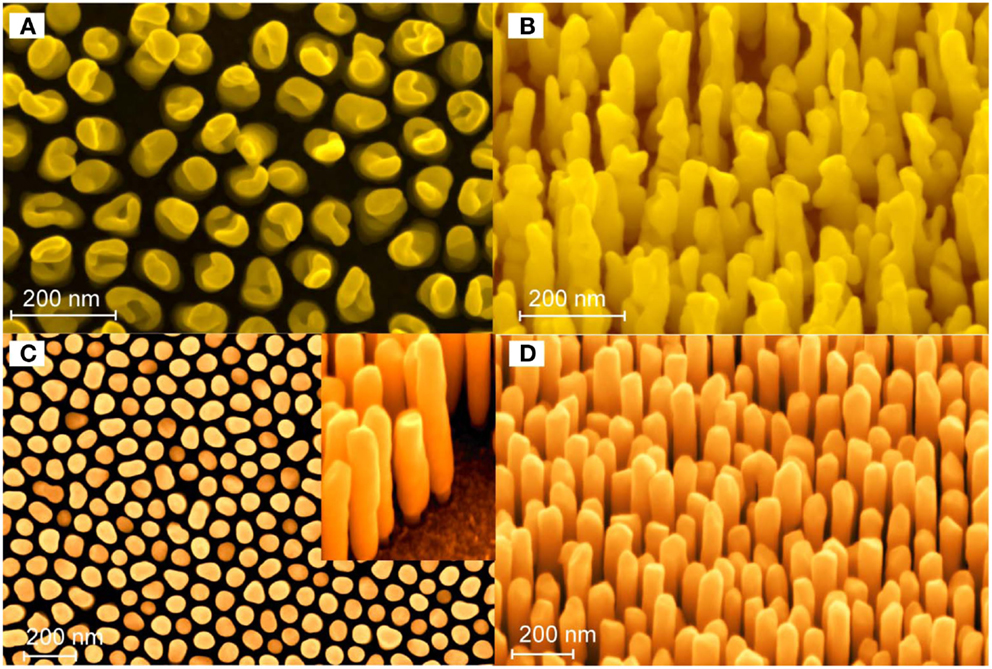
Figure 5. SEM secondary electron micrographs showing different Au-NR morphologies; (A,B) top and side views, respectively, of Au-NRs processed potentiostatically using an HAuClO4 electrolyte; (C,D) Au-NRs processed using pulsed voltage deposition and a commercial electrolyte. The diameter of the NRs is 70 nm and the gap between them varies between 30 and 50 nm (Habouti et al., 2011b).
Nanostructures of Au and Ag show peculiar absorption properties that translate in extinction maxima, not present in their bulk counterparts, the loci of which are largely dependent on morphology, dimension, and dielectric environment. These extinction maxima arise from the collective oscillation of the conduction electrons with the incident electromagnetic field, and are called localized surface plasmon resonance (LSPR). It is the shift of the LSPR peak in the presence of adsorbed (macro)molecules that is exploited in biosensing, e.g., see the review by Mayer and Hafner (2011). Further, the coupling of the LSPRs of adjacent NP, separated by small gaps of some tens of nanometers, leads to gap plasmons that can concentrate the electromagnetic field in the gap between the particles. In these so-called “hot spots,” huge field enhancements may be obtained that can be exploited in surface-enhanced resonant spectroscopies, particularly surface-enhanced Raman spectroscopy (SERS). In this context, various strategies have been implemented to fabricate SERS substrates with nanostructures of controllable and reproducible gaps, and desirable huge enhancement factors. Among the fabrication routes are bottom–up techniques that rely on chemical synthesis of NP with simple and complex geometries and their self-assembly on a substrate, e.g., using chemical lithography, and top–down techniques such as e-beam lithography, etc. [see the review article by Halas et al. (2011) and references therein; Grzelczak et al. (2010) and Yan et al. (2009)]. We think that PAAF affords a propitious route to control the dimensions, gap, and morphology of noble metal nanostructures and consequently their optical properties and SERS enhancement factors. Periodic nanostructures with individual elements showing fork-like geometries may be obtained, as shown in Figure 5 above. These structures are particularly interesting for molecular detection because they present a high density of hot spots.
The optical properties of noble metal nanostructures grown in PAAF may be tailored via control of the pore size length and periodicity. In the following example, we show how the reflectance and absorption properties of Au-NRs depend on their length and dielectric medium. With respect to periodicity effects, we have not yet succeeded in making PAAF with different interpore gaps and no related data could be found in the published literature. However, investigations on e-beam lithography processed Au-structures with varying gaps had shown that decreasing the gap between the nanostructures resulted in a redshift of the LPRs. These results were validated using finite-difference time-domain simulation (Duan et al., 2011), and should also be valid for anisotropic plasmonic nanostructures processed using PAAF. Ongoing work will bring further details on this topic.
The anisotropy of the Au-NRs leads to the splitting of their LSPR into a transverse and longitudinal mode (Wurtz et al., 2007; Mayer and Hafner, 2011). But the optical properties of whole system, i.e., PAAF on a substrate, embedded and exposed nanostructures, present far more rich features that are still to be investigated in more details, and may be exploited in photonics and sensing (Hotta et al., 2012). The diffuse reflectance spectra of a PAAF on silicon and embedded Au-NRs are displayed in Figure 6. In comparison to the spectrum of a 30 nm Au-film on the same substrate, PAAF presents interference patterns that extend well in the IR region, and represent Fabry–Perot interferences at the different interfaces involved. Deposition of Au-NRs in the pores results, as expected, in a completely different spectrum with the substantial attenuation of some interferences and the appearance of new minima. These results are similar to those obtained by Lyvers et al. (2008), and denote LSPR modes that are confined between adjacent Au-NRs embedded in the dielectric matrix, as validated by their FEM simulations. It is, however, noteworthy that the weak minimum at approximately 520 nm corresponds to the transverse plasmon mode observed for Au-NRs, while the strong minimum at approximately 900 nm is generally attributed to the longitudinal LSPR mode (that depend on the Au-NR length), although, as pointed out by Lyvers et al., the modes observed here may differ from those observed on colloidal NRs. Nevertheless, both modes were also obtained for exposed Au-NRs on a glass/5 nm Au-film substrate, Figure 7. Under the condition of normal incidence of non-polarized light, both 100 and 360 nm long Au-NRs give rise to a maximum at approximately 520 nm, whereas the second mode is distinctly observed only for the longer NRs (for the 100 nm NRs, a shoulder can be observed at about 700 nm).
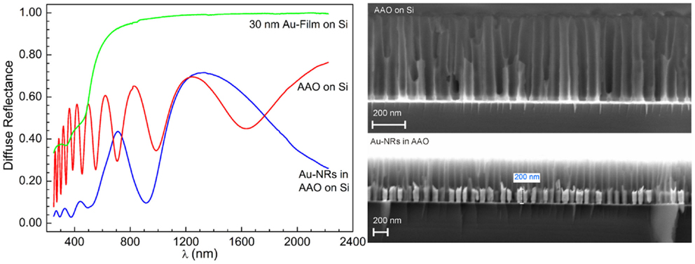
Figure 6. Diffuse reflectance spectra of empty AAO and embedded Au-NRs (SEM micrographs on the right hand) in comparison to an Au-film on Si.
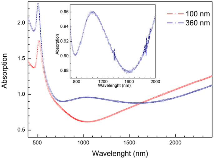
Figure 7. Absorption spectra of exposed Au-NRs of different length on a glass substrate terminated with a 5 nm Au-film. Incidence of non-polarized light is normal to the plane of the NR array. The mode at approximately 520 nm is the LSPR transverse mode. For the 360 nm long NRs, the longitudinal mode at approximately 1020 nm is distinctly observed, whereas only a shoulder at approximately 700 nm is observed for the short NRs.
Increasing the length of the Au-NR results in a large redshift in the order of 200 nm of the longitudinal LSPR toward a wave length well in the NIR region, Figure 8.
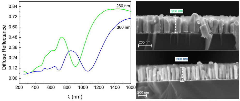
Figure 8. Diffuse reflectance spectra of embedded Au-NRs showing pronounced minima at different wave lengths, depending on Au-NR length.
For certain applications, robust nanostructures, both mechanically and thermally, are needed. PAAF is very well suited for this purpose, and can be advantageously used for embedding the nanostructures, providing at the same time a rear contact through the Au-film. In terms of noble metal nanostructures, the presence of aluminum oxide does not all too much affect the optical properties. This is well illustrated in Figure 9, which shows the very close similarity between the diffuse reflectance of embedded and exposed Au-NR film of the same length, with the exception of a small blue shift of the mode at around 700 nm. The locus of the longitudinal mode is not affected but the intensity and sharpness of the minimum is increased over the exposed Au-NRs, because of the confinement of the NRs into the nanoporous templates, thus preserving their verticality and order. These results stand somewhat in contrast to those of Lyvers et al. (2008), where a large difference in the reflectance of embedded and exposed Au-NRs is reported. This discrepancy may be amenable to the different layer thicknesses involved and the substantial thickness of the Al-oxide template still present in their embedded structures, in contrast to ours, which fill the whole PAAF thickness.
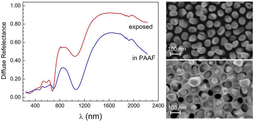
Figure 9. Diffuse reflectance spectra of embedded and exposed Au-NRs of the same length (SEM micrographs are shown on the right-hand side). “Exposed” means that the Al-oxide template has been dissolved.
Some Applications of Ordered Nanostructure Films
Some of the applications of ordered nanostructure films have been mentioned above. Substrates for molecular detection via resonant spectroscopy techniques are among the most promising applications of ordered noble metal nanostructures. Au and Ag-NR films have been used as SERS substrates with huge effective enhancement factors measured over the whole substrate. This demonstrates that PAAF is well suited for the processing of affordable SERS substrates with reproducible SERS enhancement, Figure 10 (Habouti et al., 2011a). The effect of Au-NR morphology on signal enhancement is demonstrated in Figure 11 (Habouti et al., 2011b).
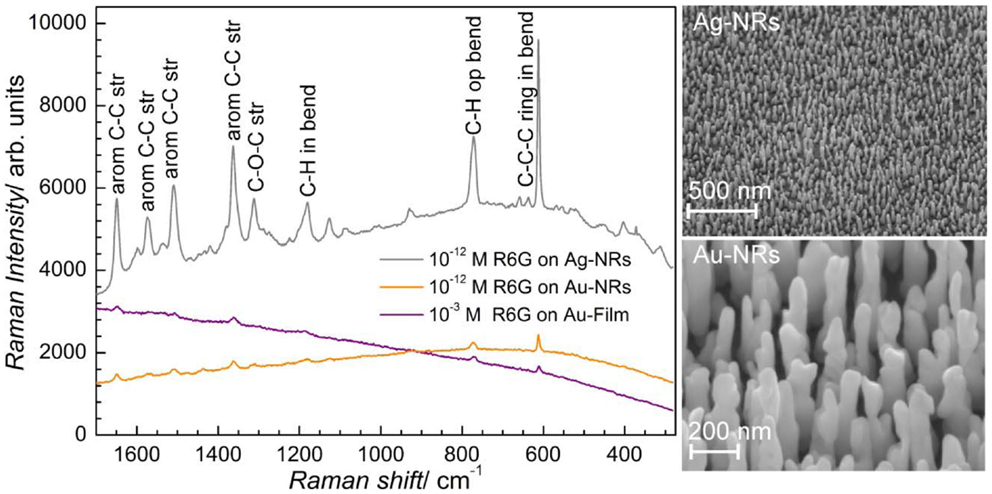
Figure 10. SERS of rhodamine 6G (R6G) on supported Ag and Au-NRs (SEM micrographs are shown on the right-hand side) (Habouti et al., 2011a).
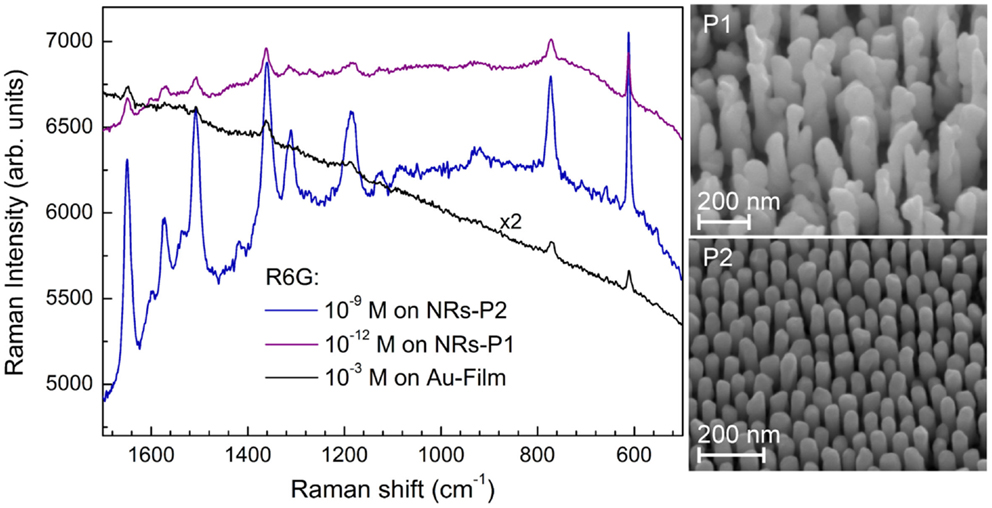
Figure 11. Morphology effects of supported Au-NR on the SERS signal of R6G. The SERS signal on P1 (corrugated morphology) is reproducible over the whole substrate while that of P2 (smooth morphology) is obtained only on isolated areas (Habouti et al., 2011b). The SEM micrographs of both morphologies are shown on the right-hand side.
The processing of composite structures consisting of plasmonic nanostructures and other functional materials, e.g., semi-conducting oxides, may result in new and efficient nanostructures for light harvesting as has been demonstrated by Mubeen et al. (2013) for supported Au-NRs/TiO2/Pt-NP nanocomposites for water splitting. Plasmonic–thermochromic nanocomposites have been reported using supported, VO2-capped Au-NRs, Figure 12. First Au-NRs were deposited on glass substrates using PAAF and, after dissolving PAAF, sputter-coated with an ultra-thin vanadium layer of 5 and 10 nm. Annealing at 450°C under nitrogen atmosphere resulted in the formation of caps of the monoclinic VO2 phase on top of the Au-NRs. This phase undergoes a reversible insulator–metal transition (monoclinic to rutile type transition) at 68–70°C in bulk form. Using the structure shown in Figure 12C, the insulator–metal-transition temperature could be decreased to values down to 45°C via a Mott–Hubbard transition mechanism involving electron injection into the conduction band of the semi-conducting phase (Habouti and Es-Souni, 2014). More promising applications may be in electrocatalysis and hydrogen gas sensing using Pt and Pd-NRs and NT (Dar et al., 2012), in electrochemical energy storage using NiO pseudocapacitor nanostructures (Dar et al., 2013), and many more.
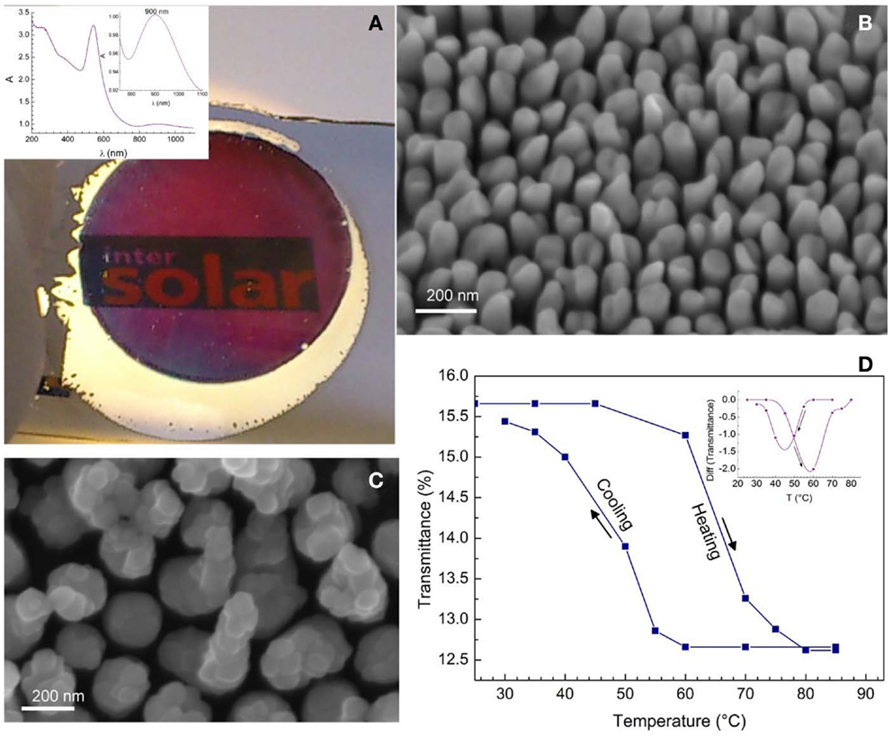
Figure 12. (A) Photograph of electrodeposited Au-NRs on glass; the surrounding, non-anodized Al-film is still to be seen; inset shows the absorption spectrum of the Au-NRs. (B) shows a SEM micrograph of the Au-NRs. (C) Composite structure of VO2 on Au-NRs. (D) Hysteresis loop on heating and cooling showing the insulator to metal transition of VO2; the inset shows the transition temperature (Habouti and Es-Souni, 2014).
Summary and Perspectives
Supported anodized aluminum oxide films can be advantageously used for the processing of ordered nanostructure films with a wide range of functionalities and applications. The main advantages of the so-processed nanostructures lie in their low cost together with robustness and easy handling. The latter may even be increased by leaving the nanostructures partially embedded in the template, which will not affect functionality for certain applications. We have shown that large-area metallic nanostructures with various morphologies and aspect ratios can easily be processed using electrochemical deposition. The process can be also up-scaled to wafer size as demonstrated in Figure 13. More ordered nanomaterials, monolithic, and composites films can be generated from self-assembly in pores and electrophoretic deposition using functionalized colloidal NP. The generated nanostructures afford high surface areas together with specific functionalities, with promising potential applications in sensing, photonics, light harvesting, and energy storing.
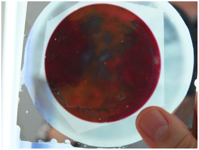
Figure 13. Au-NR film that was processed in large area, double anodized PAAF on a glass wafer. The Au-NR film is still embedded in the PAAF. The non-anodized Al-film is still seen at the edges of the wafer.
In this paper, emphasis was placed on PAAF because in our opinion only limited attention has been devoted to these templates in comparison to the well-known AAO membranes. By addressing the critical issues related to the processing of PAAF while underlying their potential for generating supported, ordered nanostructures, we hope that more interest will be devoted to them in the future. We are, however, aware that other methods such as self-assembly, eventually combined with lithographic methods, are also suitable for making sophisticated nanostructure films.
Conflict of Interest Statement
The authors declare that the research was conducted in the absence of any commercial or financial relationships that could be construed as a potential conflict of interest.
References
Camelio, S., Vandenhecke, E., Rousselet, S., and Babonneau, D. (2014). Optimization of growth and ordering of Ag nanoparticle arrays on ripple patterned alumina surfaces for strong plasmonic coupling. Nanotechnology 25, 035706. doi:10.1088/0957-4484/25/3/035706
Dar, F. I., Habouti, S., Minch, M., Dietze, M., and Es-Souni, M. (2012). Morphology control of 1D noble metal nano/heterostructures towards multi-functionality. J. Mater. Chem. 22, 8671. doi:10.1039/c2jm16826j
Dar, F. I., Moonoosawmy, K., and Es-Souni, M. (2013). Morphology and property control of NiO nanostructures for supercapacitor applications. Nanoscale Res. Lett. 8, 363. doi:10.1186/1556-276X-8-363
Duan, H., Hu, H., Kumar, K., Shen, Z., and Yang, J. K. W. (2011). Direct and reliable patterning of plasmonic nanostructures with sub-10-nm gaps. ACS Nano 5, 7593–7600. doi:10.1021/nn2025868
Foong, T. R. B., Sellinger, A., and Hu, X. (2008). Origin of the bottlenecks in preparing anodized aluminum oxide (AAO) templates on ITO glass. ACS Nano 2, 2250. doi:10.1021/nn800435n
Gates, B. D., Xu, Q., Stewart, M., Ryan, D., Willson, C. G., and Whitesides, G. M. (2005). New approaches to nanofabrication: molding, printing, and other techniques. Chem. Rev. 105, 1171. doi:10.1021/cr030076o
Gish, D. A., Summers, M. A., and Brett, M. J. (2006). Morphology of periodic nanostructures for photonic crystals grown by glancing angle deposition. Photon. Nanostruct. Fundam. Appl. 4, 23. doi:10.1016/j.photonics.2005.11.003
Grzelczak, M., Vermant, J., Furst, E. M., and Liz-Marzán, L. M. (2010). Directed self-assembly of nanoparticles. ACS Nano 4, 3591. doi:10.1021/nn100869j
Habouti, S., and Es-Souni, M. (2014). Au-NRs/VO2-NPs nanocomposites supported on glass substrates: microstructure and optical properties. CrystEngComm 16, 3068. doi:10.1039/c3ce42097c
Habouti, S., Mátéfi-Tempfli, M., Solterbeck, C.-H., Es-Souni, M. A., Mátéfi-Tempfli, S., and Es-Souni, M. (2011a). Self-standing corrugated Ag and Au-nanorods for plasmonic applications. J. Mater. Chem. 21, 6269. doi:10.1039/c0jm03459b
Habouti, S., Mátéfi-Tempfli, M., Solterbeck, C.-H., Es-Souni, M. A., Mátéfi-Tempfli, S., and Es-Souni, M. (2011b). On-substrate, self-standing Au-nanorod arrays showing morphology controlled properties. Nano Today 6, 12. doi:10.1016/j.nantod.2010.11.001
Halas, N. J., Lal, S., Chang, W.-S., Link, S., and Nordlander, P. (2011). Plasmons in strongly coupled metallic nanostructures. Chem. Rev. 111, 3913. doi:10.1021/cr200061k
Hotta, K., Yamaguchi, A., and Teramae, N. (2012). Nanoporous waveguide sensor with optimized nanoarchitectures for highly sensitive label-free biosensing. ACS Nano 6, 1541. doi:10.1021/nn204494z
Hulteen, J. C., and Martin, C. R. (1997). A general template-based method for the preparation of nanomaterials. J. Mater. Chem. 7, 1075. doi:10.1039/a700027h
Jones, M. R., Osberg, K. D., Macfarlane, R. J., Langille, M. R., and Mirkin, C. A. (2011). Templated techniques for the synthesis and assembly of plasmonic nanostructures. Chem. Rev. 111, 3736. doi:10.1021/cr1004452
Kattner, U. R., Li, J.-C., and Chang, Y. A. (1992). Thermodynamic assessment and calculation of the Ti-AI system. Metall. Trans. 23A, 2081.
Lee, W., Ji, R., Gösele, U., and Nielsch, K. (2006). Fast fabrication of long-range ordered alumina membranes by hard anodization. Nat. Mater. 5, 741. doi:10.1038/nmat1717
Li, F., Zhang, L., and Metzger, R. M. (1998). On the growth of highly ordered pores in anodized aluminum oxide. Chem. Mater. 10, 2470. doi:10.1021/cm980163a
Liu, Y.-J., Chu, H. Y., and Zhao, Y. P. (2010). Silver nanorod array substrates fabricated by oblique angle deposition: morphological, optical, and SERS characterizations. J. Phys. Chem. C 114, 8176. doi:10.1021/jp1001644
Lyvers, D. P., Moon, J.-M., Kildishev, A. V., Shalaev, V. M., and Wei, A. (2008). Gold nanorod arrays as plasmonic cavity resonators. ACS Nano 2, 2569. doi:10.1021/nn8006477
Mallet, J., Zhang, K. Y., Mátéfi-Tempfli, S., Mátéfi-Tempfli, M., and Piraux, L. (2005). Electrodeposited L10 CoxPt1- x nanowires. J. Appl. Phys. D 38, 909. doi:10.1088/0022-3727/38/6/020
Mann, S. (2009). Self-assembly and transformation of hybrid nano-objects and nanostructures under equilibrium and non-equilibrium conditions. Nat. Mater. 8, 781. doi:10.1038/nmat2496
Masuda, H., and Fukuda, K. (1995). Ordered metal nanohole arrays made by a two-step replication of honeycomb structures of anodic alumina. Science 268, 1466. doi:10.1126/science.268.5216.1466
Mátéfi-Tempfli, S., and Mátéfi-Tempfli, M. (2009). Vertically aligned nanowires on flexible silicone using a supported alumina template prepared by pulsed anodization. Adv. Mater. 21, 4005. doi:10.1002/adma.200900344
Mayer, K. M., and Hafner, J. H. (2011). Localized surface plasmon resonance sensors. Chem. Rev. 111, 3828. doi:10.1021/cr100313v
Mubeen, S., Lee, J., Singh, N., Krämer, S., Stucky, G. D., and Moskovits, M. (2013). An autonomous photosynthetic device in which all charge carriers derive from surface plasmons. Nat. Nanotechnol. 8, 247. doi:10.1038/nnano.2013.18
Murray, J. L. (1983). The Au-Ti (gold-titanium) system. Bull. Alloy Phase Diag. 4, 278. doi:10.1007/BF02868667
Piraux, L., Renard, K., Guillemet, R., Mátéfi-Tempfli, S., Mátéfi-Tempfli, M., Antohe, V. A., et al. (2007). Template-grown NiFe/Cu/NiFe nanowires for spin transfer devices. Nano Lett. 7, 2563. doi:10.1021/nl070263s
Thompson, G. E. (1997). Porous anodic alumina: fabrication, characterization and applications. Thin Solid Films 297, 192. doi:10.1016/S0040-6090(96)09440-0
Wurtz, G. A., Evans, P. R., Hendren, W., Atkinson, R., Dickson, W., Pollard, R. J., et al. (2007). Molecular plasmonics with tunable exciton-plasmon coupling strength in J-aggregate hybridized Au nanorod assemblies. Nano Lett. 7, 1297. doi:10.1021/nl070284m
Xia, Y., and Whitesides, G. M. (1998). Soft lithography. Angew. Chem. Int. Ed. 37, 550. doi:10.1002/(SICI)1521-3773(19980316)37:5<550::AID-ANIE550>3.3.CO;2-7
Keywords: film heterostructure, ordered porous films, supported templates, ordered nanostructures, anisotropic nanostructures
Citation: Es-Souni M and Habouti S (2014) Ordered nanomaterial thin films via supported anodized alumina templates. Front. Mater. 1:19. doi: 10.3389/fmats.2014.00019
Received: 08 August 2014; Paper pending published: 23 August 2014;
Accepted: 17 September 2014; Published online: 01 October 2014.
Edited by:
Antonio Politano, Università degli Studi della Calabria, ItalyReviewed by:
Gregory Abadias, Institut Pprime, FranceMuhammad Rizwan Saleem, University of Eastern Finland, Finland
Harish Barshilia, National Aerospace Laboratories, India
Copyright: © 2014 Es-Souni and Habouti. This is an open-access article distributed under the terms of the Creative Commons Attribution License (CC BY). The use, distribution or reproduction in other forums is permitted, provided the original author(s) or licensor are credited and that the original publication in this journal is cited, in accordance with accepted academic practice. No use, distribution or reproduction is permitted which does not comply with these terms.
*Correspondence: Mohammed Es-Souni, Institute for Materials and Surface Technology, University of Applied Sciences, Grenzstrasse 3, Kiel, Germany e-mail: me@fh-kiel.de