Graphene-based transparent electrodes for hybrid solar cells
 Pengfei Li
 Caiyun Chen
 Jie Zhang
 Qiaoliang Bao
- Jiangsu Key Laboratory for Carbon-Based Functional Materials and Devices, Collaborative Innovation Center of Suzhou Nano Science and Technology, Institute of Functional Nano and Soft Materials (FUNSOM), Soochow University, Suzhou, China
The graphene-based transparent and conductive films were demonstrated to be cost-effective electrodes working in organic–inorganic hybrid Schottky solar cells. Large area graphene films were produced by chemical vapor deposition on copper foils and transferred onto glass as transparent electrodes. The hybrid solar cell devices consist of solution-processed poly (3,4-ethlene-dioxythiophene): poly (styrenesulfonate) (PEDOT: PSS), which is sandwiched between silicon wafer and graphene electrode. The solar cells based on graphene electrodes, especially those doped with HNO3, have comparable performance to the reference devices using commercial indium tin oxide (ITO). Our work suggests that graphene-based transparent electrode is a promising candidate to replace ITO.
Introduction
Solar energy is a potential substitute for fossil fuels in the future because it is a renewable energy source and inexhaustible. Over a few decades, the photovoltaic industry has been grown rapidly following the improvements in the efficiency and the demand for alternative energy resources. Commercial silicon photovoltaic with the power conversion efficiency (PCE) of above 20% plays a dominate role but the high-manufacturing cost is still a major issue for large-scale implementation. Many efforts have been made to reduce the cost of photovoltaic devices. The combination of organic and inorganic materials to form a hybrid solar cell is very promising approach as it marries lower process cost of organic materials with the good performance of silicon. However, the conventional anode for organic materials, indium tin oxide (ITO), is becoming expensive because of the dwindling supplies of indium and the growth of the environmental costs (Wang et al., 2008; Novoselov et al., 2012; Son et al., 2012). The silver electrodes demonstrated in the laboratory are also not suitable for large-scale commercial usage. There are huge demands for developing new electrode materials with lower cost and comparable performance.
Graphene has been proposed to be an effective transparent electrode to replace ITO in solar cell (Bao et al., 2009; Park et al., 2011; Wang et al., 2011a; Miao et al., 2012) as graphene exhibits excellent properties such as low-sheet resistance, high transmittance, good mechanical property, and good thermal and chemical stability (Yin et al., 2014). Graphene has very high-carrier mobility as charge carriers in it are delocalized over large areas, resulting in an unencumbered platform for electron/hole transport. High Fermi-velocity and the ability to be doped chemically contribute to extremely high in-plane conductivities. As early as 2007, Wang et al. (2008) fabricated polymer solar cells using reduced graphene oxide as transparent electrode and achieved a PCE of 0.26%. Afterwards, chemical vapor deposition (CVD) approach has been used by many groups to synthesize single- or few-layer graphene films with large area for energy harvesting applications, which is a significant advance in this field. Gomez De Arco et al. (2010) reported the continuous, highly flexible, and transparent graphene films produced by CVD as transparent conductive electrodes in organic solar cells. The efficiency of organic solar cells with graphene electrode was 1.18%, which is close to that of organic solar cells with ITO electrode (~1.27%). In 2011, Wang et al. (2011a) used layer-by-layer transfer method to fabricate multilayer CVD graphene films with less defects and lower sheet resistance. The organic solar cells with the electrode of four layers graphene have an improved PCE up to 2.5%, which is 83.3% of the PCE of ITO-based devices. For the hybrid solar cell, Wu et al. (2013) demonstrated the use of graphene as transparent conductive electrodes with the structure of graphene/organic/silicon, which has a PCE of 10%. However, the solar cell has a very small device area of about 0.1 cm2.
In this work, we used graphene films as transparent electrodes to work in organic–inorganic hybrid Schottky solar cells with a relatively large device area. The hybrid solar cells based on solution-processed poly (3,4-ethlene-dioxythiophene): poly (styrenesulfonate) (PEDOT: PSS) in combination with silicon wafer are fabricated through a simple and low-cost process (Li et al., 2010; Song et al., 2012; Liu et al., 2013; Shen et al., 2013; Zhu et al., 2013). It was found that the surface doping of graphene film can effectively improve the device performance. This work suggests that the application of graphene-based transparent electrode can be extended to a wide range of new optoelectronic devices.
Materials and Methods
Growth and Transfer of Graphene Films
Large area graphene films were produced using CVD on the copper foils as the method described in the literature (Yu et al., 2010; Manu et al., 2011). We used a modified transfer method to prepared the graphene-based transparent electrode and it includes the following steps: (1) deposition of PMMA and curing; (2) etching of copper foil in FeCl3 solution and rinsing in deionized (DI) water for three times; (3) rinsing PMMA/graphene in DI water three times; (4) fishing of PMMA/graphene onto glass substrate; (5) re-deposition of one drop of PMMA solution and curing; and (6) removal of PMMA with acetone. The as-transferred graphene films were doped by putting them in the vapor of HNO3 (concentration of 69%) for 10 s.
Materials Characterizations
The morphology of the graphene film was checked by optical microscopy (Leica DM2700 M). The domain of the graphene film was indicated by scanning electron microscope (SEM Quanta 200 FEG). The quality of the graphene film was verified by Raman spectroscopy (HORIBA JOBIN-YVON LABRAM HR800). The optical property was investigated by UV–visible spectrometer (Perkin Elmer, Lambda 750). The work function of intrinsic and doped graphene film is measured using ultraviolet photoelectron spectroscopy (UPS, KRATOS Analytical).
Preparation of Silicon Wafer and PEDOT: PSS
The organic–inorganic hybrid solar cells were fabricated by n-doped Si and PEDOT: PSS. The Si wafer was first cleaned for half an hour using acetone, ethanol, and DI water. Following, the wafer was treated by chlorination and alkylation. Highly conductive PEDOT: PSS (CLEVIOS PH 1000) was incorporated with 5% wt DMSO to increase conductivity and 1% wt Triton was used as surface activator. The resulting solution was stirred thoroughly to ensure that the different chemicals are uniformly mixed (Shen et al., 2010; Zhang et al., 2011).
Fabrication of Solar Cells
Using physics vapor deposition (PVD), 0.6 nm of LiF and 200 nm of Al electrode were deposited on the back of the silicon wafer. Then PEDOT: PSS was spin-coated onto the silicon wafer and the graphene/glass. (Speed: 4000 rpm, time: 1 min) The resulted organic films (about 70–80 nm thick) was then annealed at 125°C for 30 min in a glove box (Shen et al., 2013; Zhu et al., 2013). The last step is the encapsulation of the solar cell devices, in which a clamp and AB glue were used to firmly stick the graphene/glass and silicon wafer together.
Results
Preparation and Characterizations of Graphene Films
Figure 1 schematically shows the procedures to prepare graphene transparent electrode. Graphene grown on copper was transferred onto glass substrate using PMMA as a supporting host. The PMMA layer can be further cleaned by annealing the resulted sample in inert gas at above 350°C. Multilayer graphene films can be prepared by repeating the procedures in Figures 1A–D and stacking the PMMA supported graphene onto graphene covered glass.
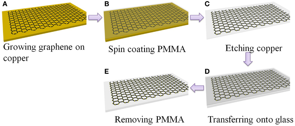
Figure 1. Schematic of transfer graphene onto glass substrate. (A) Synthesis of graphene on copper foil, (B) spin-coating of PMMA onto the Cu foil to protect graphene, (C) etching of Cu, (D) transfer of graphene/PMMA film onto glass, (E) removal of PMMA in acetone.
Figure 2A shows the optical image of single layer graphene transferred onto SiO2 wafer. It is found that the graphene film is generally uniform with fewer cracks. Figure 2B shows the SEM image of graphene film grown on copper substrate, indicating very large graphene domains on copper grains. In order to further check the quality of as-produced graphene film, Raman spectrum was measured, as shown in Figure 2C. We can clearly see two characteristic peaks: 2D peak at 2687 cm−1, which is originated from the phonon resonance and G peak at 1579 cm−1, which is correlated to the crystallinity of graphene (Ferrari et al., 2006). The intensity of 2D peak is about two times that of G peak, suggesting that the graphene synthesized on the copper foils is single layer. There is no obvious D peak at around 1350 cm−1, indicating very less defects or disorders. Figure 2D displays the Raman mapping image of intensity ratio of G/2D over an area of 5 μm × 5 μm. It is revealed that G/2D ratio is almost below 0.5 over the whole area, indicating the nature of single atomic layer (Bao et al., 2011).
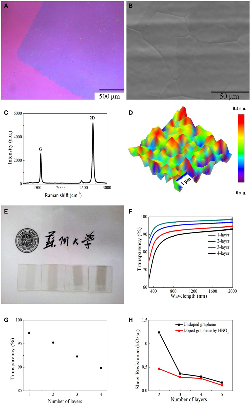
Figure 2. (A) Optical image of monolayer graphene on SiO2 substrate. (B) SEM of graphene film grown on copper substrate. (C) Raman spectrum of monolayer graphene measured on silicon substrate. (D) G/2D peak Raman map of monolayer graphene. (E) Photograph of one to four layers graphene films covering on quartz substrates. (F) Transmittance spectra of graphene with different numbers of layers. (G) Optical transparency of graphene film as a function of number of layers. (H) Sheet resistance of the undoped and doped graphene films with different numbers of layers.
Figure 2E shows the photograph of one to four layers of graphene on quartz substrates. With the increasing of the number of layers, the contrast becomes darker from left to right. Figure 2F shows the transmittance spectra from visible to near-infrared range. The smoothness of the transmittance spectrum for each graphene sample suggests that the films are generally uniform. The transmittance decreases as the number of layers (see Figure 2G) in graphene increases, i.e., each additional layer results in a decrease of about 2.3% in the transmittance, which is due to the universal absorption of graphene film shows in Figure 2F. We also found that the sheet resistance of both undoped and doped graphene is reduced while increasing the number of layers, as shown in Figure 2H.
Characterizations of the Solar Cells
Figure 3A shows the schematic structure of the hybrid Schottky solar cells with graphene electrode. The cross-section of the device reveals a vertical structure where PEDOT: PSS is sandwiched between and n-type silicon. Figure 3B shows the photographs of real solar cell device. Both the top view and bottom view are presented. In order to standardize the photovoltaic measurements, a mask is used to expose an area of 0.5 cm × 0.5 cm for light illumination, as shown in Figure 3C.
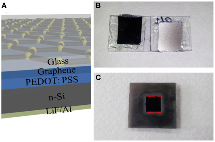
Figure 3. (A) Schematic diagrams of hybrid solar cells using graphene as electrode. The cross-section of solar cell shows different functional layers. (B) Photograph of the real hybrid solar cell device after encapsulation. Left: top view; right: bottom view. (C) Photograph of solar cell device covered with a mask.
Figure 4 shows the output characteristics and external quantum efficiency (EQE) of doped graphene-based hybrid solar cells under AM1.5G illumination. The JSC of the devices is above 22 mA/cm2 and the average circuit voltage (Voc) is about 0.55 ± 0.2 V. The detailed performance results are summarized in Table 1. For 2-layer and 3-layer graphene films, the same fill factor is obtained; however, 3-layer graphene gives higher PCE and the highest JSC (25.09 mA/cm2). Overall, 4-layer graphene gives the highest fill factor and PCE. It may result from a lower sheet resistance in the 3-layer and 4-layer graphene. It is generally found that the fill factor and PCE are increased while increasing the number of graphene layers. This may be attributed to the reduction of the sheet resistance as well as the improved contact between graphene layers and PEDOT: PSS. This trend agrees with the observed trend in literatures (Wang et al., 2011a). However, it should be noted that the performance of different batches of devices is also different due to many unpredictable factors during the device fabrication. By optimizing the graphene film quality, balancing the optical transparency with conductivity and the fill factor, it is possible to obtain a relatively high efficiency from these hybrid Schottky solar cells.
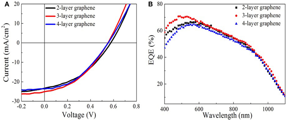
Figure 4. Characterizations of graphene-based hybrid solar cells. (A) The current density versus voltage (J–V) curve of solar cells with two to four layers graphene electrodes. (B) External quantum efficiency of the solar cells.
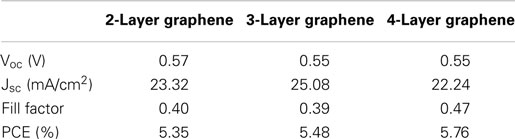
Table 1. The parameters of solar cells made from doped graphene electrodes with different thicknesses.
In order to further study the effect of sheet resistance and work function of graphene on the solar cell performance, we compare the devices based on undoped graphene with those based on doped graphene. It is well known that HNO3 could cause p-type doping in graphene, which improves the conductivity and charge transfer efficiency (Wang et al., 2011b; Feng et al., 2012; Miao et al., 2012; Cui et al., 2013). Figure 5A shows the photovoltaic characteristics and Table 2 lists the detailed performance parameters. Figure 5B shows the schematic energy diagram of the hybrid solar cell device. The down-shift of Fermi level in graphene (p-type doping) will facilitate the collection of photo-excited holes from PEDOT: PSS/Si hetero-junction. Interestingly, the PCE of graphene-based solar cell is improved by 40% after doping with HNO3, as illustrated in Table 2. This is understandable because the doping treatment causes the sheet resistance to decrease from 320 to 247 Ω/□ (see Table 3). Another consequence of doping is that the short-circuit current (Jsc) of the graphene-based solar cell increases from 22.88 to 25.08 mA/cm2 (see Table 2).
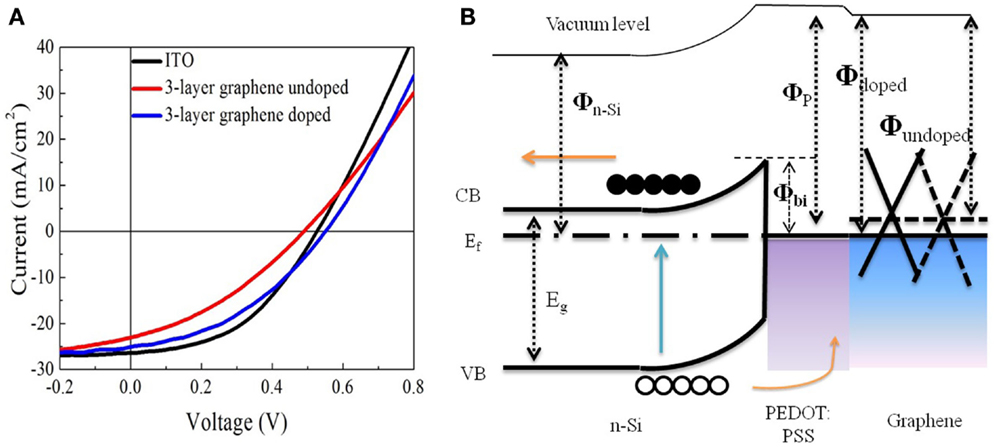
Figure 5. (A) J–V curves of the solar cells based on graphene and ITO electrodes. (B) Schematic energy diagram of the hybrid solar cell device.
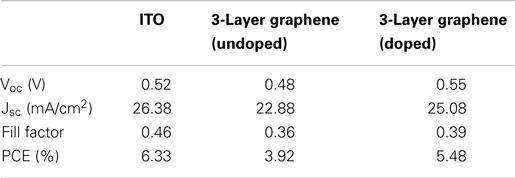
Table 2. The parameters of the different solar cells based on graphene and ITO electrodes.
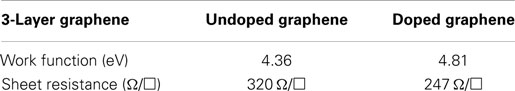
Table 3. The work function and sheet resistance of 3-layer graphene before and after doped by HNO3.
The engineering of work function of graphene by doping also plays an important role to affect the final device performance. As shown in Table 3, the measured work function of 3-layer graphene is increased from 4.36 to 4.81 eV. The Voc of the solar cell before the doping of graphene is lower than that of ITO-based solar cell, however, it is increased from 0.48 to 0.55 V but after the doping, which is even higher than that of ITO-based solar cell. As a result, the PCE of graphene-based solar cell is enhanced from 3.92 to 5.48%. Using ITO-based hybrid solar cell as a reference, it is found that doped graphene electrode can deliver comparable energy conversion performance (Wang et al., 2011a), 3-layer graphene electrode gives a PCE of 5.48%, which is about 87% of that of ITO. There is still much space to improve for graphene-based electrode as the sheet resistance of ITO is ~100 Ω/□ or less. However, considering rising price of ITO because of the dwindling supplies of indium, graphene films, with additional chemical tunability, could be a very promising candidate to replace ITO as transparent electrode in solar cells.
The degradation in solar cells is also a very important figure of merit to evaluate the device performance. We tested the ITO and graphene electrode solar cells after 1 month storage in dry cabinet. Figure 6 and Table 4 show the results before and after 1 month. It is found that both the solar cell with graphene and that with ITO experience a decrease in PCE after a month. The fill factor of both solar cells is decreased by almost 6.3%. The Jsc of ITO-based solar cell is decreased from 25.64 to 22.4 mA/cm2 and the Voc is decreased from 0.53 to 0.50 V. In contrast, the Voc and Jsc of the graphene-based device have a relatively smaller decrease, from 0.55 to 0.54 V and from 25.09 to 23.49 mA/cm2, respectively. Consequently, the PCE of ITO-based solar cell is decreased by 22.7% and that of graphene-based solar cell is decreased by 11.7% only. Therefore, it is concluded that graphene-based hybrid solar cell device degrade slower than ITO-based hybrid solar cell. It may correlate to good chemical compatibility of graphene with organic molecular such as PEDOT: PSS and this is an interesting topic in demand of further investigation.
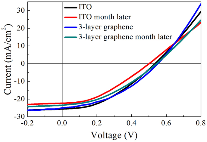
Figure 6. J–V curves of the solar cells measured before and after 1 month.
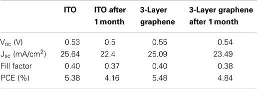
Table 4. The degradation of different solar cells with ITO and graphene electrodes.
Conclusion
The graphene-based thin films were successfully applied as transparent electrodes working in organic–inorganic hybrid Schottky solar cells. In comparison to similar solar cell devices using ITO as electrodes, graphene-based solar cells can deliver comparable photovoltaic performance. It is found that the chemical doping by HNO3 can effectively increase the work function, reduce the sheet resistance, which in turn improve the solar cell performance. The lifetime study suggests that graphene-based solar cell experiences smaller degradation than ITO-based device. This work indicates that graphene-based electrodes have the potential to replace ITO in a wide range of optoelectronic devices.
Conflict of Interest Statement
The authors declare that the research was conducted in the absence of any commercial or financial relationships that could be construed as a potential conflict of interest.
Acknowledgments
This work was supported by the National High Technology Research and Development Program of China (863 Program) (Grant No. 2013AA031903), the youth 973 program (2015CB932700), the National Natural Science Foundation of China (Grant No. 51222208, 51290273), the Doctoral Fund of Ministry of Education of China (Grant No. 20123201120026).
References
Bao, Q., Zhang, H., Ni, Z., Wang, Y., Polavarapu, L., Shen, Z., et al. (2011). Monolayer graphene as a saturable absorber in a mode-locked laser. Nano Res. 4, 297–307. doi:10.1364/OL.38.001745
Pubmed Abstract | Pubmed Full Text | CrossRef Full Text | Google Scholar
Bao, Q., Zhang, H., Wang, Y., Ni, Z., Yan, Y., Shen, Z. X., et al. (2009). Atomic-layer graphene as a saturable absorber for ultrafast pulsed lasers. Adv. Funct. Mater. 19, 3077–3083. doi:10.1002/adfm.200901007
Cui, T., Lv, R., Huang, Z.-H., Chen, S., Zhang, Z., Gan, X., et al. (2013). Enhanced efficiency of graphene/silicon heterojunction solar cells by molecular doping. J. Mater. Chem. A 1, 5736–5740. doi:10.1039/c3ta01634j
Feng, T., Xie, D., Lin, Y., Zhao, H., Chen, Y., Tian, H., et al. (2012). Efficiency enhancement of graphene/silicon-pillar-array solar cells by HNO3 and PEDOT-PSS. Nanoscale 4, 2130–2133. doi:10.1039/c2nr12001a
Pubmed Abstract | Pubmed Full Text | CrossRef Full Text | Google Scholar
Ferrari, A. C., Meyer, J. C., Scardaci, V., Casiraghi, C., Lazzeri, M., Mauri, F., et al. (2006). Raman spectrum of graphene and graphene layers. Phys. Rev. Lett. 97, 187401. doi:10.1103/physrevlett.97.187401
Gomez De Arco, L., Zhang, Y., Schlenker, C. W., Ryu, K., Thompson, M. E., and Zhou, C. (2010). Continuous, highly flexible, and transparent graphene films by chemical vapor deposition for organic photovoltaics. ACS Nano 4, 2865–2873. doi:10.1021/nn901587x
Pubmed Abstract | Pubmed Full Text | CrossRef Full Text | Google Scholar
Li, X., Zhu, H., Wang, K., Cao, A., Wei, J., Li, C., et al. (2010). Graphene-on-silicon Schottky junction solar cells. Adv. Mater. Weinheim 22, 2743–2748. doi:10.1002/adma.200904383
Liu, D., Zhang, Y., Fang, X., Zhang, F., Song, T., and Sun, B. (2013). An 11%-power-conversion-efficiency organic-inorganic hybrid solar cell achieved by facile organic passivation. Electron Dev. Lett. IEEE 34, 345–347. doi:10.1109/LED.2013.2239255
Manu, J., Xuan, L. C. H. Y., Qiaoliang, B., Tat, T. C., Ping, L. K., and Barbaros, O. (2011). Controlled hydrogenation of graphene sheets and nanoribbons. ACS Nano 5, 888–896. doi:10.1021/nn102034y
Pubmed Abstract | Pubmed Full Text | CrossRef Full Text | Google Scholar
Miao, X., Tongay, S., Petterson, M. K., Berke, K., Rinzler, A. G., Appleton, B. R., et al. (2012). High efficiency graphene solar cells by chemical doping. Nano Lett. 12, 2745–2750. doi:10.1021/nl204414u
Pubmed Abstract | Pubmed Full Text | CrossRef Full Text | Google Scholar
Novoselov, K. S., Fal, V., Colombo, L., Gellert, P., Schwab, M., and Kim, K. (2012). A roadmap for graphene. Nature 490, 192–200. doi:10.1038/nature11458
Park, H., Brown, P. R., Bulović, V., and Kong, J. (2011). Graphene as transparent conducting electrodes in organic photovoltaics: studies in graphene morphology, hole transporting layers, and counter electrodes. Nano Lett. 12, 133–140. doi:10.1021/nl2029859
Pubmed Abstract | Pubmed Full Text | CrossRef Full Text | Google Scholar
Shen, X., Sun, B., Yan, F., Zhao, J., Zhang, F., Wang, S., et al. (2010). High-performance photoelectrochemical cells from ionic liquid electrolyte in methyl-terminated silicon nanowire arrays. ACS Nano 4, 5869–5876. doi:10.1021/nn101980x
Pubmed Abstract | Pubmed Full Text | CrossRef Full Text | Google Scholar
Shen, X., Zhu, Y., Song, T., Lee, S.-T., and Sun, B. (2013). Hole electrical transporting properties in organic-Si Schottky solar cell. Appl. Phys. Lett. 103, 013504. doi:10.1063/1.4812988
Son, D. I., Kwon, B. W., Park, D. H., Seo, W.-S., Yi, Y., Angadi, B., et al. (2012). Emissive ZnO-graphene quantum dots for white-light-emitting diodes. Nat. Nanotechnol. 7, 465–471. doi:10.1038/nnano.2012.71
Pubmed Abstract | Pubmed Full Text | CrossRef Full Text | Google Scholar
Song, T., Lee, S.-T., and Sun, B. (2012). Silicon nanowires for photovoltaic applications: the progress and challenge. Nano Energy 1, 654–673. doi:10.1016/j.nanoen.2012.07.023
Wang, X., Zhi, L., and Müllen, K. (2008). Transparent, conductive graphene electrodes for dye-sensitized solar cells. Nano Lett. 8, 323–327. doi:10.1021/nl072838r
Pubmed Abstract | Pubmed Full Text | CrossRef Full Text | Google Scholar
Wang, Y., Tong, S. W., Xu, X. F., Özyilmaz, B., and Loh, K. P. (2011a). Interface engineering of layer-by-layer stacked graphene anodes for high-performance organic solar cells. Adv. Mater. Weinheim 23, 1514–1518. doi:10.1002/adma.201190044
Wang, Y., Tong, S. W., Xu, X. F., Ozyilmaz, B., and Loh, K. P. (2011b). Interface engineering of layer-by-layer stacked graphene anodes for high-performance organic solar cells. Adv. Mater. 23, 1514–1518. doi:10.1002/adma.201190044
Wu, Y., Zhang, X., Jie, J., Xie, C., Zhang, X., Sun, B., et al. (2013). Graphene transparent conductive electrodes for highly efficient silicon nanostructures-based hybrid heterojunction solar cells. J. Phys. Chem. C 117, 11968–11976. doi:10.1021/jp402529c
Yin, Z., Zhu, J., He, Q., Cao, X., Tan, C., Chen, H., et al. (2014). Graphene-based materials for solar cell applications. Adv. Energy Mater. 4, 1–19. doi:10.1002/aenm.201300574
Yu, W., Xiangfan, X., Jiong, L., Ming, L., Qiaoliang, B., Barbaros, Ö, et al. (2010). Toward high throughput interconvertible graphane-to-graphene growth and patterning. ACS Nano 4, 6146–6152. doi:10.1021/nn1017389
Pubmed Abstract | Pubmed Full Text | CrossRef Full Text | Google Scholar
Zhang, F., Sun, B., Song, T., Zhu, X., and Lee, S. (2011). Air stable, efficient hybrid photovoltaic devices based on poly(3-hexylthiophene) and silicon nanostructures. Chem. Mater. 23, 2084–2090. doi:10.1021/cm103221a
Keywords: graphene, hybrid Schottky solar cell, transparent electrode, indium tin oxide
Citation: Li P, Chen C, Zhang J, Li S, Sun B and Bao Q (2014) Graphene-based transparent electrodes for hybrid solar cells. Front. Mater. 1:26. doi: 10.3389/fmats.2014.00026
Received: 08 August 2014; Accepted: 22 October 2014;
Published online: 06 November 2014.
Edited by:
Xiaobin Fan, Tianjin University, ChinaReviewed by:
Thiagarajan Soundappan, Washington University in St. Louis, USAQiang Zhang, Tsinghua University, China
Junyi Ji, Sichuan University, China
Copyright: © 2014 Li, Chen, Zhang, Li, Sun and Bao. This is an open-access article distributed under the terms of the Creative Commons Attribution License (CC BY). The use, distribution or reproduction in other forums is permitted, provided the original author(s) or licensor are credited and that the original publication in this journal is cited, in accordance with accepted academic practice. No use, distribution or reproduction is permitted which does not comply with these terms.
*Correspondence: Qiaoliang Bao, Jiangsu Key Laboratory for Carbon-Based Functional Materials and Devices, Collaborative Innovation Center of Suzhou Nano Science and Technology, Institute of Functional Nano and Soft Materials (FUNSOM), Soochow University, Suzhou 215123, China e-mail: qlbao@suda.edu.cn, qiaoliang.bao@gmail.com