Direct growth of Ge1−xSnx films on Si using a cold-wall ultra-high vacuum chemical-vapor-deposition system
 Aboozar Mosleh1,2*
  Murtadha A. Alher2,3
 Larry C. Cousar1,4
Wei Du2
Larry C. Cousar1,4
Wei Du2
 Seyed Amir Ghetmiri1,2
Thach Pham2
Seyed Amir Ghetmiri1,2
Thach Pham2
 Joshua M. Grant5
Greg Sun6
Richard A. Soref6
Baohua Li4
Hameed A. Naseem2
Joshua M. Grant5
Greg Sun6
Richard A. Soref6
Baohua Li4
Hameed A. Naseem2  Shui-Qing Yu2
- 1Microelectronics-Photonics Graduate Program (μEP), University of Arkansas, Fayetteville, AR, USA
- 2Department of Electrical Engineering, University of Arkansas, Fayetteville, AR, USA
- 3Mechanical Engineering Department, University of Karbala, Karbala, Iraq
- 4Arktonics, LLC, Fayetteville, AR, USA
- 5Engineering-Physics Department, Southern Arkansas University, Magnolia, AR, USA
- 6Department of Engineering, University of Massachusetts Boston, Boston, MA, USA
Germanium–tin alloys were grown directly on Si substrate at low temperatures using a cold-wall ultra-high vacuum chemical-vapor-deposition system. Epitaxial growth was achieved by adopting commercial gas precursors of germane and stannic chloride without any carrier gases. The X-ray diffraction analysis showed the incorporation of Sn and that the Ge1−xSnx films are fully epitaxial and strain relaxed. Tin incorporation in the Ge matrix was found to vary from 1 to 7%. The scanning electron microscopy images and energy-dispersive X-ray spectra maps show uniform Sn incorporation and continuous film growth. Investigation of deposition parameters shows that at high flow rates of stannic chloride the films were etched due to the production of HCl. The photoluminescence study shows the reduction of band-gap from 0.8 to 0.55 eV as a result of Sn incorporation.
Introduction
The discovery and development of Ge1−xSnx epitaxy technology has enabled silicon photonics to be explored in a different scope of a material platform. The ability of band-gap engineering by varying Sn mole fraction, along with its compatibility to the complementary metal–oxide–semiconductor (CMOS) process, has paved the way for highly competitive Si-based near and mid-infrared optoelectronic devices. Recent reports on the fabrication and characterization of high performance Ge1−xSnx devices such as modulators (Kouvetakis et al., 2005), photodetectors (Conley et al., 2014a,b), and light emitting diodes (LEDs) (Du et al., 2014a) show great potential for Ge1−xSnx being adopted by industry in the near future. Cutting-edge reports on Ge1−xSnx, achieving a direct band-gap group IV alloy (Du et al., 2014b; Ghetmiri et al., 2014a; Li et al., 2014; Wirths et al., 2014), is a turning point for the technology to be pursued for the demonstration of an efficient group IV laser. In addition, due to the tunable lattice constant and formation of Lomer dislocations, Ge1−xSnx has been shown to work as a universal compliant buffer layer to grow high quality lattice mismatched materials, like III–Vs, on Si (Beeler et al., 2011a; Mosleh et al., 2014).
A variety of challenges exist for the growth of Ge1−xSnx alloys on Si such as large lattice mismatch between Ge1−xSnx and Si (more than 4.2%), low solid solubility of Sn in Ge (less than 0.5%), and instability of diamond lattice Sn (α-Sn) above 13°C. Therefore, growth can only possibly be done under non-equilibrium conditions. Different growth methods have been demonstrated for Ge1−xSnx growth in which molecular beam epitaxy (MBE) and chemical-vapor-deposition (CVD) have obtained device quality material and high Sn incorporation. For the MBE method, both gas source and solid source MBE have been used by different groups to grow Ge1−xSnx films (Gurdal et al., 1998; Takeuchi et al., 2007; Chen et al., 2011; Werner et al., 2011; Stefanov et al., 2012; Bhargava et al., 2013; Oehme et al., 2013; Wang et al., 2013).
The other parallel approach of Ge1−xSnx growth is CVD. The early results of CVD growth by Kouvetakis and Chizmeshya (2007) at Arizona State University (ASU) showed the ability to grow Ge1−xSnx film directly on Si using a hot-wall ultra-high vacuum CVD (UHV-CVD) system with deuterated Stannane (SnD4) as the Sn precursor along with different chemistries of germanium. Due to the high cost and instability of SnD4, other precursors such as tetramethyl tin [Sn(CH3)4] and stannic chloride (SnCl4) have been explored to grow Ge1−xSnx alloys. Vincent et al. (2011) (from IMEC using atmospheric pressure CVD) and Kim et al. (Chen et al., 2013) [from Applied Materials/Stanford University using reduced pressure-CVD (RP-CVD)] have reported successful growth of Ge1−xSnx by using SnCl4 and a high cost Ge precursor digermane (Ge2H6) and carrier gases on a Ge-buffered Si substrate. Using the same SnCl4 and Ge2H6 precursors and carrier gases, Mantl et al. (Wirths et al., 2013) (from PGI9-IT) demonstrated direct growth of Ge1−xSnx on Si using showerhead technology in an RP-CVD chamber. In the recent report, Tolle et al. (Margetis et al., 2014; Mosleh et al., 2014a) (ASM company) have achieved Ge1−xSnx growth using an industry prevail RP-CVD reactor in collaboration with University of Arkansas (UA). Low-cost Germane (GeH4) and SnCl4 with carrier gasses of N2/H2 were used to grow Ge1−xSnx. A Ge buffer was deposited between the Si substrate and the Ge1−xSnx layer in order to compensate the lattice mismatch between the layers. Table 1 lists the different research groups that have grown Ge1−xSnx using CVD. Different growth methods and the cost effectiveness of the gas precursors are compared.
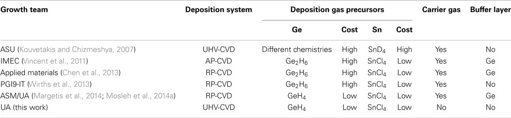
Table 1. A summary of reports on Ge1−xSnx growth using CVD methods by different research groups.
In this paper, we report direct growth of strain-relaxed Ge1−xSnx films on Si substrates with Sn mole fractions up to 7% using a cold-wall UHV-CVD system. Stannic chloride and germane were chosen as the precursors which are low-cost and commercially available. The growth of Ge1−xSnx films was achieved without using any carrier gases and buffer layers. In order to investigate the material quality, the X-ray diffraction (XRD), high-resolution transmission electron microscopy (TEM), energy-dispersive X-ray spectroscopy (EDX), Raman spectroscopy, and photoluminescence (PL) measurements have been conducted.
Experiment
Growth Method
A cold-wall UHV-CVD system was adopted to grow Ge1−xSnx films (see Figure 1 for machine schematic). The system composes a load-lock chamber with a base pressure of 10−6 Pa and a process chamber whose base pressure reaches 10−8 Pa using the turbo-molecular and cryogenic pumps, respectively. Due to low-temperature growth of the films, removal of oxygen and water vapor is critical which was achieved by using a cryogenic pump. The turbo-molecular pumps are backed by mechanical pumps. The heating stage consisted of a pyrolytic graphite heater with a thermocouple placed at the same distance away from the heater as the wafer. The sample holder rotates up to 80 rpm for uniform film growth. The gas flow is through a side entry port, controlled by mass flow controllers (MFCs). Stannic chloride is a volatile liquid with vapor pressure of 2.4 kPa at one atmospheric pressure. Therefore, the evaporation could produce enough pressure to be passed through the MFC.
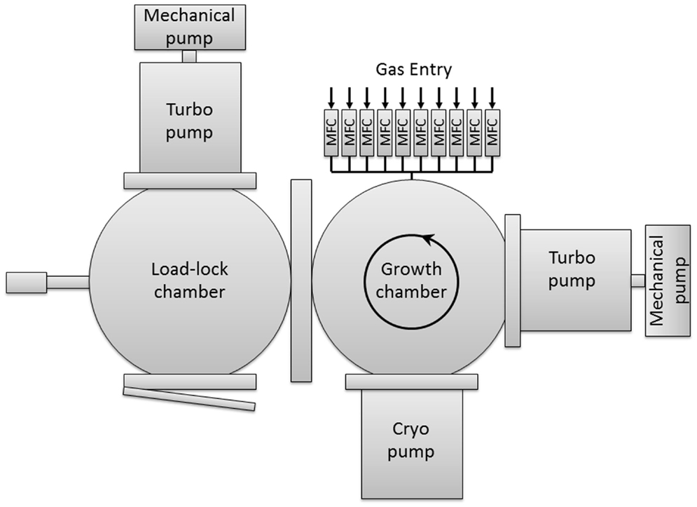
Figure 1. Cold-wall UHV-CVD system with a substrate rotation. Samples are transferred through a load-lock chamber equipped with a turbo-molecular pump. The growth chamber is equipped with a turbo-molecular pump and a cryogenic pump. Side entry of the gases is controlled by mass flow controllers.
Germanium–tin films were grown on 4″ (001) p-type Si substrates with 5–10 Ω cm resistivity. Prior to loading the samples, they were cleaned in a two-step process: (1) Piranha etch solution [H2SO4:H2O2 (1:1)], (2) oxide strip HF dipping [H2O:HF (10:1) using 48% pure HF] followed by nitrogen blow drying. The final oxide strip step was not followed by a water rinse as it reduces the life-time of hydrogen passivation and exposes the surface to ambient oxygen (Mosleh et al., 2013, 2014b). The experiments were carried out at reduced pressures of 13, 40, 65, 95, 130, 200, and 260 Pa and at temperatures as low as 300°C. Germane (GeH4) and stannic chloride (SnCl4) were used as the precursors for Ge1−xSnx growth. The gas flow ratio (GeH4/SnCl4) was set to 5, 3.3, 2.5, and 1.6. Depending on the growth parameters such as gas flow ratio and deposition pressure, a growth rate of 20–3.3 nm/min was achieved.
Characterization Method
Analysis of Sn mole fraction, lattice constant, growth quality, and strain in the Ge1−xSnx films were conducted using a high-resolution X-ray diffractometer. High-resolution TEM (TITAN) with an accelerating voltage of 300 kV was used to investigate crystal orientation and defects in the grown epi-layers as well as determining the thicknesses of the samples. Surface morphology of the samples was investigated by a scanning electron microscope equipped with EDX. Room temperature PL measurements were carried out using a 690-nm excitation laser. The PL signal was collected by a grating-based spectrometer equipped with a thermoelectric-cooled PbS detector (cut-off at 3 μm) for spectral analysis.
Results and Discussion
Material Characterization
The 2θ-ω XRD scan was performed from the symmetric (004) plane to obtain the out-of-plane lattice constant of the Ge1−xSnx films. Figure 2A shows the peak at 69° corresponding to a satisfaction of the Bragg condition by Si (001) substrate, and the peaks at lower angles of 66–65° due to larger lattice size of the Ge1−xSnx layers. The difference in the position of Ge1−xSnx peaks is due to the difference in the Sn mole fractions of Ge1−xSnx layers. Different compositions were achieved from 1 to 7% with desirable crystal quality. The Ge1−xSnx peaks are broadened for two reasons: (1) thin film thickness of the layers and (2) presence of mosaicity in the Ge–Sn crystal and formation of defects as a result of strain relaxation. The full width at half maximum (FWHM) of the Ge1−xSnx peaks are between 0.28 for 1% Sn film and 0.36 for 7% Sn film. The change in FWHM depends on various factors such as film thickness, relaxation, and quality and there is no trend showing that the FWHM of the peaks change as the Sn composition increases.
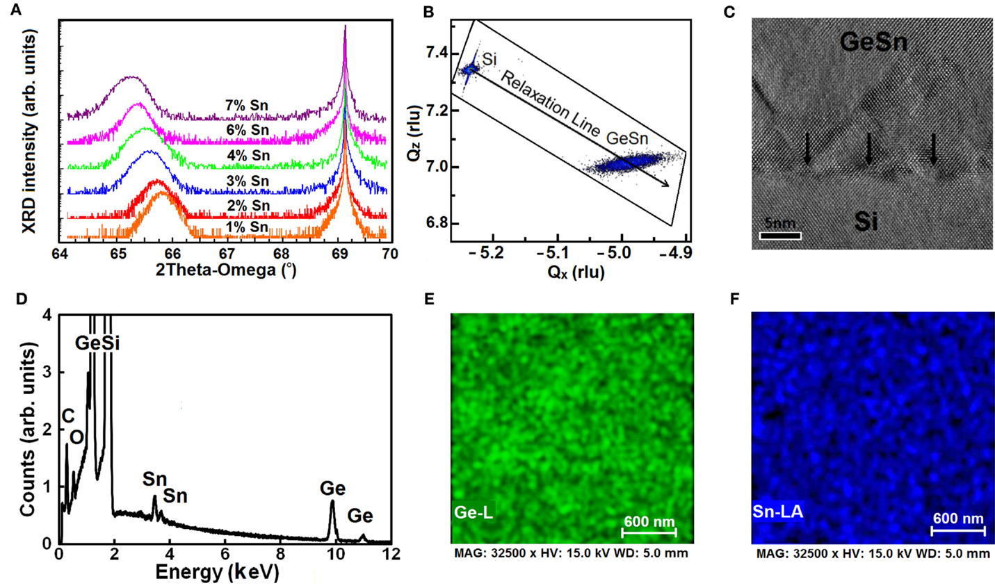
Figure 2. (A) Symmetric (004) 2θ-ω scan of Ge1−xSnx films which are grown on a Si substrate. The peak at 69° shows the Si substrate peak and the peaks between 66° and 65° belong to Ge1−xSnx films. (B) Reciprocal space map from asymmetrical plane (−2, −2, 4) for Ge0.94Sn0.06 grown on a Si substrate. The x-coordinate shows out-of-plane lattice constant and the y-coordinate shows in-plane lattice constant in units of reciprocal lattice unit. The relaxation line shows that the films grown above are tensile strained and below are compressively strained. Presence of the Ge0.94Sn0.06 on the relaxation line shows that the film is strain relaxed. (C) Transmission electron microscopy images of Ge0.94Sn0.06 film shows epitaxial growth of Ge–Sn on a Si substrate. Arrows show misfit dislocations formed at the Ge1−xSnx/Si interface. (D) The EDX spectrum of Si/Ge0.94Sn0.06 film shows the presence of Si (substrate), Ge and Sn (film), O (native oxide), and C (carbon contamination from the ambient). (E) The EDX surface maps of Ge and (F) Sn taken from scanning electron micrographs for Ge0.94Sn0.06 film shows uniform growth of Ge1−xSnx alloy.
In order to calculate the total lattice constant and the strain in the film, an asymmetric reciprocal space mapping (RSM) from (−2, −2, 4) plane was performed. The RSM scans provide measurement of the in-plane (a∥) and out-of-plane (a⊥) lattice constant of Ge1−xSnx alloys. The total lattice constant was calculated by taking into account the elastic constants of Ge1−xSnx (Beeler et al., 2011b). Knowing the total lattice constant, the Sn mole fractions is calculated through Vegard’s law with the bowing factor of b = 0.0166 Å (Moontragoon et al., 2012). Figure 2B shows the RSM of 6% Sn sample. The x-axis shows Qz in reciprocal lattice unit (rlu) which is related to the out-of-plane lattice constant (L) and the y-axis shows Qx which is related to the in-plane lattice constant (H or K). Direction of the spread in the Ge0.94Sn0.06 peak does not show a compositional gradient in the sample because it is related to the relaxation of the lattice on Si substrate. Large lattice mismatch between Sn and Ge is the main reason for a large spread in the omega direction. The relaxation line in Figure 2B shows that the films which are grown above are tensile strained and the films grown underneath are compressively strained. The Ge0.94Sn0.06 peak is observed to be on the relaxation line and the relaxation is measured to be 97%.
Calculation of total strain in other samples shows that all the films are more than 95% relaxed. Table 2 shows the lattice constants of the Ge1−xSnx alloys, their Sn mole fraction, and strain relaxation percentage. Ge1−xSnx films were almost fully relaxed mainly due to large lattice mismatch between Si (5.431 Å) and Ge1−xSnx (above 5.658 Å) and small critical thickness (Mosleh et al., 2014a). The other reason for relaxation of Ge (and similarly Ge1−xSnx) films on Si is the thermal mismatch between these two materials. High temperature growth (above 500°C) and rapid cool down has been the main method for achieving tensile strained Ge on Si (Conley et al., 2014a). The Ge1−xSnx samples were grown at 300°C for 30 min and we have not achieved tensile strained films; however, the thermal mismatch between Si and Ge1−xSnx has helped relaxing the compressive strain. The strain has been mainly relieved through formation of misfit dislocations including Lomer misfit dislocation. The cross-sectional TEM image in Figure 2C shows formation of such dislocations at the Ge1−xSnx/Si interface. In addition, Figure 2B shows that strain relaxation occurred by formation of misfit dislocations at the interface. The TEM image shows that the grown film was fully epitaxial. Film thickness of the samples is listed in Table 2.
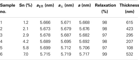
Table 2. Tin mole fraction calculation, lattice constant, and relaxation percentage of the grown samples.
The SEM scan/EDX spectra of the samples show surface morphology of the sample as well as Sn incorporation in the Ge matrix. The EDX spectra in Figure 2D show the presence of Ge, Si, and Sn in the Ge0.94Sn0.06 film. Due to the high count collection of secondary electrons from the substrate, the ratio of Sn and Ge cannot exactly reveal the percentage of Sn in Ge. The presence of carbon and oxygen in the EDX spectra is mainly due to the contamination and oxidation of the film after exposure to ambient air. The EDX maps for Ge (Figure 2E) and Sn (Figure 2F) display uniform incorporation of Sn. The SEM image shows continuous growth of Ge1−xSnx without observation of locally crystalline patches. No segregation and precipitation of Sn was observed on the films which indicates robust and stable growth of the films.
Growth Mechanism
Growth of Ge1−xSnx on a Si substrate requires considering the reaction of byproducts and reduction of activation energy by introducing carrier gases. Stannic chloride has a tendency to etch Ge due to the presence of chlorine in the chemistry of the molecule. The byproduct of GeH4 + SnCl4 reaction is HCl which is an etchant gas for germanium and silicon (Bogumilowicz et al., 2005). Following reactions show different mechanisms of film deposition as well as HCl production in the chamber:
Higher temperature of the substrate results in higher density of depositing ad-atoms (Ge and Sn); however, it will result in production of HCl at a higher rate. In addition, higher flow rate of SnCl4 increases the production rate of HCl as well. Controlling the temperature and flow rate of the gases could control the process so that growth is the dominant process in the chamber. The Ge/Sn film will be etched by HCl through the following reactions:
Domination of etching over growth is the main mechanism that prevents direct growth of Ge1−xSnx on Si.
By controlling the flow through MFCs, we have grown Ge1−xSnx films on Si at different pressures with a fixed flow ratio of GeH4/SnCl4 = 1.6. Growth was observed at 13 Pa of deposition pressure and continued until the deposition pressure increased to 130 Pa. Figure 3A shows the thickness of Ge1−xSnx films versus deposition pressure of the chamber as well as Sn incorporation percentage. Incorporation of Sn in the Ge lattice is increased by raising the pressure due to the higher residence time of the precursors in the chamber. The residence time of the gases has increased from 2 s at 13 Pa to 19 s at 130 Pa. Meanwhile, HCl etched more of the Ge1−xSnx films after deposition at higher pressures. This trend has continued to 130 Pa and no growth has been observed at 200 and 265 Pa. The increase in Sn composition from 1 to 6% has been accompanied with reduction in the thickness from 615 to 108 nm. Films that were expected to have higher than 6% Sn content were totally etched off. Therefore, in order to grow higher Sn content films, growth mechanism under fixed pressure and changing the SnCl4 flow was studied. Higher film thickness and higher Sn incorporation was achieved as a result of domination of growth over etching. Figure 3B shows Sn incorporation in Ge1−xSnx films versus SnCl4 flow rate at 95 Pa deposition pressure. The secondary axis of Figure 3B shows film thicknesses of the samples. Due to the dominance of etching for higher SnCl4 flow rate, the films were mostly etched and the film thickness was less than 100 nm.
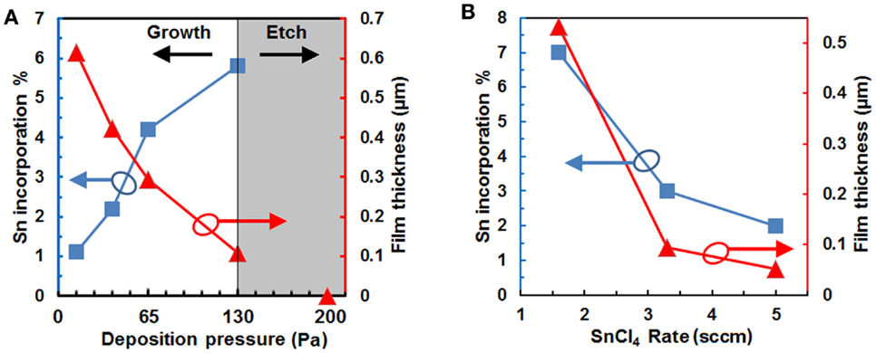
Figure 3. (A) Variation of Sn incorporation percentage versus deposition pressure. Films were etched away for deposition pressures higher than 130 Pa. The secondary axis on the right shows the reduction of film thickness as a result of increase in the deposition pressure. (B) Tin incorporation and film thickness of the samples grown at 65 Pa growth pressure versus GeH4/SnCl4 flow ratios.
Introduction of carrier gases has different effects on the growth of Ge1−xSnx films. Hydrogen changes the balance in the reaction to produce more HCl. Consequently, the GeH4/SnCl4 ratio at which the Ge1−xSnx films were depositing will not result in growth when hydrogen is introduced in the chamber. In addition, introduction of nitrogen and argon as carrier gases will reduce the activation energy of the growth (Wirths et al., 2013). Although reduction of activation energy enables easier breakdown of the molecules on the surface and enhances the growth quality and growth rate, it would prepare the conditions for easier etch due to the presence of an etchant agent. Therefore, the presence of carrier gases pushes the competition between growth and etching toward etching, resulting in film etching at even lower flow rates of carrier gases when the flow rate of SnCl4 is of the same order of GeH4.
Optical Characterization
Raman spectroscopy
The Ge1−xSnx films were further investigated by Raman spectroscopy in order to analyze the crystal structure. Room temperature Raman spectra of the grown samples as well as a Ge reference sample are plotted in Figure 4A. The Ge–Ge longitudinal optical (LO) peak was observed at 300 cm−1 for the Ge reference sample while the Ge–Ge peak in the Ge1−xSnx films was shifted to lower wavenumbers due to the change in bonding energy of Ge–Ge by incorporation of Sn atoms. The intensity of the Ge–Ge LO peak at 300 cm−1 is normalized for all the samples for comparison of the peak positions. In addition to the main Ge–Ge peak, Raman spectra of Ge1−xSnx films show other peaks that are induced as a result of Sn incorporation. The Ge–Sn LO peaks for different Sn mole fractions were observed at 250–260 cm−1 in the films. A second peak of Ge–Sn is observed at 285 cm−1, which can be seen as a shoulder of Ge–Ge main peak.
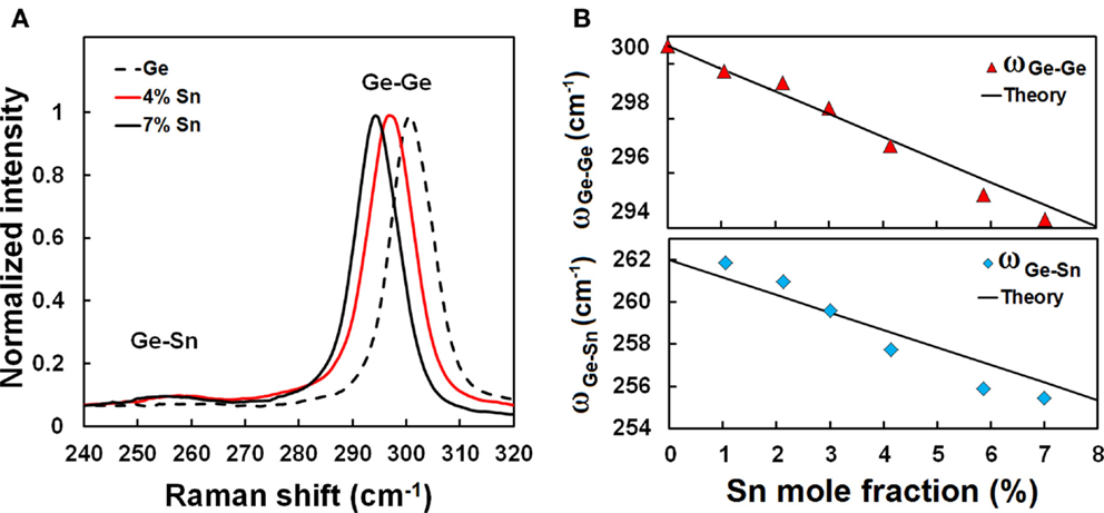
Figure 4. (A) Raman spectra of the Ge1−xSnx film grown on a Si substrate. The shift in the Ge–Ge peak is due to the incorporation of Sn in Ge lattice. The shoulder on the left side of the Ge–Ge peak is due to the Ge–Sn peak at 285 cm−1. The Ge–Sn peak is shown at lower wavenumber of 250–260 cm−1. (B) Ge–Ge and Ge–Sn peak shifts versus Sn mole fraction. The solid symbols are experimental data and the curves are theoretical predictions for relaxed films. The Ge–Ge peak is expected to shift 0.8310 cm−1 for every 1% Sn incorporation in relaxed films. The expected shift (0.8311 cm−1) for Ge–Sn peak is very close to that of Ge–Ge.
The peak positions are obtained by Lorentzian fitting to find the exact position for further analysis. The shift in the Ge–Ge LO peak depends on both strain and Sn composition of the films. Theoretical calculations for Δω are different for strain-relaxed films and strained films for different Sn (x) content [ΔωGe−Ge(x) = bx cm−1]. The Ge–Ge peak is expected to shift by a factor of b = −30.30 for a strained alloy while this factor varies to b = −83.10 for a strain-relaxed film (Cheng et al., 2013). Figure 4B shows the experimental data obtained for Ge–Ge and Ge–Sn Raman shift from the sample compared with the theoretical calculations. The peak shifts match well with the theoretical calculations for strain-relaxed films.
Photoluminescence
Germanium has an indirect band-gap in the L valley with the energy of 0.644 eV and a direct band-gap at the γ point with 0.8 eV energy at room temperature. Incorporation of Sn in Ge lattice lowers the conduction band edge at the γ-point at a faster rate than that at the L-point. PL measurements on Ge1−xSnx samples allow determination of the band-gap edge for various Sn compositions.
Figure 5 depicts room temperature PL intensity spectra for as-grown Ge1−xSnx films with 2, 4, 6, and 7% Sn mole fractions. As indicated in Figure 5A, increase of the Sn mole fraction results in a band-gap reduction. Both direct and indirect PL peaks exhibit red-shift with Sn compositions increase from 2 to 7%. A Gaussian fitting function was employed to extract the PL peak positions of both direct and indirect transitions as described in Ghetmiri et al. (2014b). In Ge0.94Sn0.06 and Ge0.93Sn0.07 samples, the energies difference between direct and indirect transitions are very small, therefore the PL emissions from these indirect and direct transitions cannot be identified. A temperature-dependent study is needed to differentiate the direct and indirect peak positions which will be reported in the future. The PL peaks from the samples with 2, 4, 6, and 7% Sn compositions are shown in Figure 5B as solid symbols. The solid and the dashed lines show the direct and indirect band-gap energies based on bowed Vegard’s law for the relaxed Ge1−xSnx alloy (Ghetmiri et al., 2014b), respectively. Since the Ge1−xSnx films are almost strain-free, as confirmed by XRD measurements, the experimental results closely follow the predicted values from Vegard’s law.
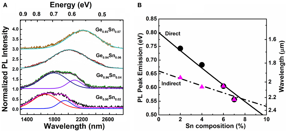
Figure 5. (A) Photoluminescence spectra of the Ge1−xSnx films with 2, 4, 6, and 7% Sn mole fraction showing a red-shift in the band-gap of the films. Incorporation of Sn has shifted both direct band-gap and indirect band-gap toward lower energies. (B) The bowed Vegard’s law interpolation for the direct (solid line) and indirect band-gap (dash line) of Ge1−xSnx alloy is plotted for different Sn compositions and is overlaid with experimental data (solid symbols).
Conclusion
Direct growth of Ge1−xSnx layers on Si substrates was achieved using a cold-wall UHV-CVD system. The films were grown by employing low-cost commercial available GeH4 and SnCl4 precursors without using any carrier gases and buffer layers. Characterizations of the samples with XRD showed successful incorporation of Sn up to 7%. The TEM images show fully epitaxial growth of the samples without any precipitation of Sn from the Ge lattice. The Raman results verified the Sn incorporation and PL measurements showed reduction of the band-gap to 0.55 eV for 7% Sn sample. The low-cost and CMOS compatible growth method and the performance of the samples indicate a promising future for Ge1−xSnx applications in Si photonics. Moreover, the samples were grown strain-relaxed enabling this material to be a universal compliant buffer layer which can be used in hybrid integration.
Conflict of Interest Statement
The authors declare that the research was conducted in the absence of any commercial or financial relationships that could be construed as a potential conflict of interest.
Acknowledgments
The work at the UA was supported by NSF (EPS-1003970), the Arkansas Bioscience Institute, the Arktonics, LLC (Air Force SBIR, FA9550-14-C-0044, Dr. Gernot Pomrenke, Program Manager), and DARPA (W911NF-13-1-0196, Dr. Dev Palmer, Program Manager). Drs. RS and GS acknowledge support from AFOSR (FA9550-14-1-0196, Dr. Gernot Pomrenke, Program Manager). JG acknowledges the support of NSF REU Program under Grant number EEC-1359306.
References
Beeler, R. T., Grzybowski, G. J., Roucka, R., Jiang, L., Mathews, J., Smith, D. J., et al. (2011a). Synthesis and materials properties of Sn/P-doped Ge on Si (100): photoluminescence and prototype devices. Chem. Mater. 23, 4480–4486. doi: 10.1021/cm201648x
Beeler, R., Roucka, R., Chizmeshya, A., Kouvetakis, J., and Menéndez, J. (2011b). Nonlinear structure-composition relationships in the Ge1-ySnySi (100) (y < 0.15) system. Phys. Rev. B 84, 035204. doi:10.1103/PhysRevB.84.035204
Bhargava, N., Coppinger, M., Gupta, J. P., Wielunski, L., and Kolodzey, J. (2013). Lattice constant and substitutional composition of GeSn alloys grown by molecular beam epitaxy. Appl. Phys. Lett. 103, 041908. doi:10.1063/1.4816660
Bogumilowicz, Y., Hartmann, J. M., Truche, R., Campidelli, Y., Rolland, G., and Billon, T. (2005). Chemical vapour etching of Si, SiGe and Ge with HCl; applications to the formation of thin relaxed SiGe buffers and to the revelation of threading dislocations. Semicond. Sci. Technol. 20, 127. doi:10.1088/0268-1242/20/2/004
Chen, R., Huang, Y., Gupta, S., Lin, A. C., Sanchez, E., Kim, Y., et al. (2013). Material characterization of high Sn-content, compressively-strained GeSn epitaxial films after rapid thermal processing. J. Cryst. Growth 365, 29–34. doi:10.1016/j.jcrysgro.2012.12.014
Chen, R., Lin, H., Huo, Y., Hitzman, C., Kamins, T. I., and Harris, J. S. (2011). Increased photoluminescence of strain-reduced, high-Sn composition Ge1-xSnx alloys grown by molecular beam epitaxy. Appl. Phys. Lett. 99, 181125. doi:10.1063/1.3658632
Cheng, R., Wang, W., Gong, X., Sun, L., Guo, P., Hu, H., et al. (2013). Relaxed and strained patterned germanium-tin structures: a Raman scattering study. ECS J. Solid State Sci. Technol. 2, 138–145. doi:10.1149/2.013304jss
Conley, B. R., Mosleh, A., Ghetmiri, S. A., Du, W., Soref, R. A., Sun, G., et al. (2014a). Temperature dependent spectral response and detectivity of GeSn photoconductors on silicon for short wave infrared detection. Opt. Express 22, 15639–15652. doi:10.1364/OE.22.015639
Pubmed Abstract | Pubmed Full Text | CrossRef Full Text | Google Scholar
Conley, B. R., Margetis, J., Du, W., Tran, H., Mosleh, A., Ghetmiri, S. A., et al. (2014b). Si based GeSn photoconductors with a 1.63 A/W peak responsivity and a 2.4 μm long-wavelength cutoff. App. Phys. Lett. 105, 221117. doi:10.1063/1.4903540
Du, W., Zhou, Y., Ghetmiri, S. A., Mosleh, A., Conley, B. R., Nazzal, A., et al. (2014a). Room-temperature electroluminescence from Ge/Ge1-xSnx/Ge diodes on Si substrates. Appl. Phys. Lett. 104, 241110. doi:10.1063/1.4884380
Du, W., Ghetmiri, S. A., Conley, B. R., Mosleh, A., Nazzal, A., Soref, R. A., et al. (2014b). Competition of optical transitions between direct and indirect bandgaps in Ge1-xSnx. Appl. Phys. Lett. 105, 051104. doi:10.1063/1.4892302
Ghetmiri, S. A., Du, W., Margetis, J., Mosleh, A., Cousar, L., Conley, B. R., et al. (2014a). Direct-bandgap GeSn grown on Silicon with 2230 nm photoluminescence. Appl. Phys. Lett. 105, 151109. doi:10.1063/1.4898597
Ghetmiri, S. A., Du, W., Conley, B. R., Mosleh, A., Naseem, H. A., Yu, S., et al. (2014b). Shortwave-infrared photoluminescence from Ge1-xSnx thin films on silicon. J. Vac. Sci. Technol. B 32, 060601. doi:10.1116/1.4897917
Gurdal, O., Desjardins, P., Carlsson, J., Taylor, N., Radamson, H., Sundgren, J., et al. (1998). Low-temperature growth and critical epitaxial thicknesses of fully strained metastable Ge1-xSnx (x ≲0.26) alloys on Ge (001) 2 × 1. J. Appl. Phys. 83, 162–170. doi:10.1063/1.366690
Kouvetakis, J., and Chizmeshya, A. V. G. (2007). New classes of Si-based photonic materials and device architectures via designer molecular routes. J. Mater. Chem. 17, 1649–1655. doi:10.1039/b618416b
Kouvetakis, J., Menendez, J., and Soref, R. A. Strain-Engineered Direct-Gap Ge/SnxGe1-x Heterodiode and Multi-Quantum-Well Photodetectors, Laser, Emitters and Modulators Grown on SnySizGe1-y-z Buffered Silicon. United States patent US 6897471 B1 (2005).
Li, H., Brouillet, J., Salas, A., Chaffin, I., Wang, X., and Liu, J. (2014). Low temperature geometrically confined growth of pseudo single crystalline GeSn on amorphous layers for advanced optoelectronics. ECS Trans. 64, 819–827. doi:10.1149/06406.0819ecst
Margetis, J., Ghetmiri, S. A., Du, W., Conley, B. R., Mosleh, A., Soref, R., et al. (2014). Growth and characterization of epitaxial Ge1-XSnx alloys and heterostructures using a commercial CVD system. ECS Trans. 64, 1830–1830. doi:10.1149/06406.0711ecst
Moontragoon, P., Soref, R., and Ikonic, Z. (2012). The direct and indirect bandgaps of unstrained Six Ge1-xySny and their photonic device applications. J. Appl. Phys. 112, 073106–8. doi:10.1063/1.4757414
Mosleh, A., Benamara, M., Ghetmiri, S. A., Conley, B. R., Alher, M. A., Du, W., et al. (2014). Investigation on the formation and propagation of defects in GeSn thin films. ECS Trans. 64, 1845–1845. doi:10.1149/06406.0895ecst
Mosleh, A., Ghetmiri, S. A., Conley, B. R., Abu-Safe, H., Waqar, Z., Benamara, M., et al. (2013). “Nucleation-step study of silicon homoepitaxy for low-temperature fabrication of Si solar cells,” in Photovoltaic Specialists Conference (PVSC), IEEE 39th. Tampa, FL.
Mosleh, A., Ghetmiri, S. A., Conley, B. R., Hawkridge, M., Benamara, M., Nazzal, A., et al. (2014a). Material characterization of Ge1-xSnx alloys grown by a commercial CVD system for optoelectronic device applications. J. Electron. Mater. 43, 938–946. doi:10.1007/s11664-014-3089-2
Mosleh, A., Ghetmiri, S. A., Conley, B. R., Abu-Safe, H. H., Benamara, M., Waqar, Z., et al. (2014b). Investigation of growth mechanism and role of H2 in very low temperature Si epitaxy. ECS Trans. 64, 967–975. doi:10.1149/06406.0967ecst
Oehme, M., Buca, D., Kostecki, K., Wirths, S., Holländer, B., Kasper, E., et al. (2013). Epitaxial growth of highly compressively strained GeSn alloys up to 12.5% Sn. J. Cryst. Growth 384, 71–76. doi:10.1016/j.jcrysgro.2013.09.018
Stefanov, S., Conde, J., Benedetti, A., Serra, C., Werner, J., Oehme, M., et al. (2012). Laser synthesis of germanium tin alloys on virtual germanium. Appl. Phys. Lett. 100, 104101. doi:10.1063/1.3692175
Takeuchi, S., Sakai, A., Yamamoto, K., Nakatsuka, O., Ogawa, M., and Zaima, S. (2007). Growth and structure evaluation of strain-relaxed Ge1-xSn buffer layers grown on various types of substrates. Semicond. Sci. Technol. 22, S231. doi:10.1088/0268-1242/22/1/S54
Vincent, B., Gencarelli, F., Bender, H., Merckling, C., Douhard, B., Petersen, D. H., et al. (2011). Undoped and in-situ B doped GeSn epitaxial growth on Ge by atmospheric pressure-chemical vapor deposition. Appl. Phys. Lett. 99, 152103–3. doi:10.1063/1.3645620
Wang, L., Su, S., Wang, W., Gong, X., Yang, Y., Guo, P., et al. (2013). Strained germanium–tin (GeSn) p-channel metal-oxide-semiconductor field-effect-transistors (p-MOSFETs) with ammonium sulfide passivation. Solid State Electron. 83, 66–70. doi:10.1016/j.sse.2013.01.031
Werner, J., Oehme, M., Schmid, M., Kaschel, M., Schirmer, A., Kasper, E., et al. (2011). Germanium-tin pin photodetectors integrated on silicon grown by molecular beam epitaxy. Appl. Phys. Lett. 98, 061108–3. doi:10.1063/1.3555439
Wirths, S., Buca, D., Mussler, G., Tiedemann, A., Holländer, B., Bernardy, P., et al. (2013). Reduced pressure CVD growth of Ge and Ge1-xSnx alloys. ECS J. Solid State Sci. Technol. 2, N99–N102. doi:10.1149/2.006305jss
Keywords: chemical-vapor-deposition, Si photonics, Ge alloys, photoluminescence, Ge–Sn
Citation: Mosleh A, Alher MA, Cousar LC, Du W, Ghetmiri SA, Pham T, Grant JM, Sun G, Soref RA, Li B, Naseem HA and Yu S-Q (2015) Direct growth of Ge1−xSnx films on Si using a cold-wall ultra-high vacuum chemical-vapor-deposition system. Front. Mater. 2:30. doi: 10.3389/fmats.2015.00030
Received: 28 January 2015; Accepted: 23 March 2015;
Published online: 27 April 2015.
Edited by:
Jifeng Liu, Dartmouth College, USAReviewed by:
Fabio Iacona, National Research Council, ItalyChristophe Labbé, Ecole Nationale Supérieure d’Ingénieurs de Caen, France
Copyright: © 2015 Mosleh, Alher, Cousar, Du, Ghetmiri, Pham, Grant, Sun, Soref, Li, Naseem and Yu. This is an open-access article distributed under the terms of the Creative Commons Attribution License (CC BY). The use, distribution or reproduction in other forums is permitted, provided the original author(s) or licensor are credited and that the original publication in this journal is cited, in accordance with accepted academic practice. No use, distribution or reproduction is permitted which does not comply with these terms.
*Correspondence: Aboozar Mosleh, Engineering Research Center (ENRC), 700 Research Center Boulevard, Fayetteville, AR 72701, USA e-mail: amosleh@gmail.com