Gate-Stack Engineering for Self-Organized Ge-dot/SiO2/SiGe-Shell MOS Capacitors
 Wei-Ting Lai1,2
 Pei-Wen Li
- 1Department of Electronics Engineering, National ChiaoTung University, HsinChu, Taiwan
- 2Department of Electrical Engineering, National Central University, ChungLi, Taiwan
We report the first-of-its-kind, self-organized gate-stack heterostructure of Ge-dot/SiO2/SiGe-shell on Si fabricated in a single step through the selective oxidation of a SiGe-nanopatterned pillar over a Si3N4 buffer layer on a Si substrate. Process-controlled tunability of the Ge-dot size (7.5–90 nm), the SiO2 thickness (3–4 nm), and the SiGe-shell thickness (2–15 nm) have been demonstrated, enabling a practically achievable core building block for Ge-based metal-oxide-semiconductor (MOS) devices. Detailed morphologies, structural, and electrical interfacial properties of the SiO2/Ge-dot and SiO2/SiGe interfaces were assessed using transmission electron microscopy, energy dispersive X-ray spectroscopy, and temperature-dependent high/low-frequency capacitance-voltage measurements. Notably, NiGe/SiO2/SiGe and Al/SiO2/Ge-dot/SiO2/SiGe MOS capacitors exhibit low interface trap densities of as low as 3–5 × 1011 cm−2 eV−1 and fixed charge densities of 1–5 × 1011 cm−2, suggesting good-quality SiO2/SiGe-shell and SiO2/Ge-dot interfaces. In addition, the advantage of having single-crystalline Si1−xGex shell (x > 0.5) in a compressive stress state in our self-aligned gate-stack heterostructure has great promise for possible SiGe (or Ge) MOS nanoelectronic and nanophotonic applications.
Introduction
Heterostructures of SiO2/Si have been the microstructural heart of metal-oxide-semiconductor (MOS) devices that have dominated integrated circuit (IC) technology since its inception nearly 60 years ago. There are mind-boggling numbers of MOS devices in production for applications ranging from logic, memory, computing, and power devices. One of the most important applications for MOS transistors is that they are key enablers for low-power circuits that are implemented in complementary MOS (CMOS) technology. In line with the relentless miniaturization of feature sizes for MOS transistors and in order to achieve desired device performance, many types of high-mobility semiconductor channels (Heyns and Tsai, 2009; Doornbos and Passlack, 2010; Oktyabrsky et al., 2010; del Alamo, 2011; Gu et al., 2011; Gupta et al., 2011; del Alamo et al., 2013) and high-k dielectric materials (Brunco et al., 2008a; Kamata, 2008; Yu et al., 2009; Xie et al., 2012) have been proposed for the replacement of the SiO2/Si gate stack. The inclusion of thin, strained layers of Si1− xGex into Si CMOS technology is one of the preeminent approaches to boost the performance of MOS transistors for both cost-effectiveness and compatibility with state-of-the-art Si technology (Wu and Li, 2007; Brunco et al., 2008a; Swaminathan et al., 2009; Toriumi et al., 2009; Yu et al., 2009; Lee et al., 2011; Nishimura et al., 2011; Zhang et al., 2012; Takenaka et al., 2013).
The production of high-quality, strained SiGe- or Ge-on-Si MOSFETs has been challenging, in particular, in situations where conventional, high-temperature thermal oxidation processes are involved. For example, during the thermal oxidation process for fabricating the conventional Ge MOSFET gate structure, the interfaces, either between Ge and Si or between Ge and the gate dielectric layers, are susceptible to defect formation (Brunco et al., 2008a; Kamata, 2008). This is because of the large lattice mismatch of 4.2% that exists between Ge and Si as well as the fact that GeOx is both water-soluble and thermally unstable, all of which are key detriments to good device performance. To date, Ge-based pMOSFETs have been extensively studied and have demonstrated superior hole mobility over Si devices. Excellent charge transfer characteristics coupled with low Dit of ~1–5 × 1011 cm−2 eV−1 have been reported for the Ge/GeO2 or Ge/GeO2/high-k MOSFETs (Swaminathan et al., 2009; Lee et al., 2011; Nishimura et al., 2011; Zhang et al., 2012; Takenaka et al., 2013). However, these characteristics were derived after the additional expense of special interfacial treatments prior to and following gate oxidation, such as postoxidation annealing (Zhang et al., 2012; Takenaka et al., 2013), two-step oxidation (Lee et al., 2011), high-pressure oxidation (Nishimura et al., 2011), and H2O oxidant prepulsing (Swaminathan et al., 2009). Additionally, all processing temperatures are constrained to be below 500°C in order to prevent GeO desorption that severely deteriorates the Ge/dielectric interface and the thermal stability of the Ge MOSFETs (Lee et al., 2011; Nishimura et al., 2011; Takenaka et al., 2013).
Realistically, gains made from improving individual transistors have not yet contributed to satisfactory improvement in the overall performance of ICs. This is because tight-packing and miniaturized metal wires lead to severe information latency and higher power consumption (Haurylau et al., 2007). Proposed solutions to overcome this looming interconnect crisis include replacing the long electrical interconnects with optical interconnects (Heck et al., 2011; Vlasov, 2015). Among possible semiconductor material choices for Si-based photonics, Ge is also the most promising candidate for active photonic devices on Si, thanks to its pseudo-direct gap electronic structure and compatibility with CMOS fabrication processes. Micrometer-scale-thick Ge-on-Si photonics, such as waveguide-coupled photodetectors (Liu et al., 2006; Assefa et al., 2010; Wang et al., 2011; Going et al., 2015; Sorianello et al., 2015), electro-absorption modulators (Chaisakul et al., 2012; Feng et al., 2012; Ren et al., 2012), and light sources (Liu et al., 2010, 2012; Camacho-Aguilera et al., 2012) have demonstrated their effectiveness and functionality. However, given their micrometer scales, these Ge/Si heterostructures are too thick to be directly integrated with the prevailing submicron or even nanometer-scale-thick Si electronic devices.
Recently, we have demonstrated a unique MOS gate-stack structure for Ge MOS devices consisting of a self-organized SiO2/Ge-dot/SiO2/SiGe-shell over the Si substrate that is achieved in a single fabrication step (Chien et al., 2011; Kuo et al., 2012, 2015; Wang et al., 2013; Chen et al., 2014; Lai et al., 2015). Our approach is primarily based on the exquisite control available through lithographic patterning combined with the selective oxidation of Si1− xGex nano-pillars over buffer layers of Si3N4 deposited over the Si substrates. Remarkably, our MOS gate-stack structure is generated in a single-step process, effectively eliminating complicated microfabrication processes, such as surface treatments and cleaning prior to the deposition of dielectrics onto the Ge. Importantly, our MOS gate stack possesses good tunability for the Ge-dot size, the interfacial SiO2 thickness, and the SiGe-shell thickness, thus providing a core building block for practical Ge-based MOS nanoelectronic and nanophotonic devices. We have also successfully exploited the use of this unique heterostructure for the production of Al/SiO2/Ge-dot/SiO2/SiGe floating-dot transistors with good charge retention/endurance (Lai et al., 2015) and for the fabrication of ITO/SiO2/Ge-dot/SiO2/SiGe MOS phototransistors with superior photoresponsivity and very low dark currents (Kuo et al., 2015). In order to further design and realize high-performance Ge MOS nanoelectronic and nanophotonic devices, it is essential to investigate the interfacial properties of the SiO2/Ge dot and the SiO2/SiGe shell within this gate-stack heterostructure of SiO2/Ge-dot/SiO2/SiGe-shell. In this paper, we have fabricated two kinds of Ge MOS capacitors: NiGe-gate/SiO2/SiGe and Al/SiO2/Ge-dot/SiO2/SiGe for the characterization of interfacial properties of the SiO2/SiGe shell and SiO2/Ge dot, respectively.
Materials and Methods
The fabrication of our MOS structure starts with a tri-layer, sequential low-pressure chemical vapor deposition of 25-nm-thick Si3N4, 70-nm-thick poly-Si0.85Ge0.15, and finally a capping layer of 5-nm-thick SiO2 over a Si substrate. The topmost SiO2/poly-Si0.85Ge0.15 layers are then lithographically patterned to create nano-cylindrical poly-Si0.85Ge0.15 pillars with a pillar density of 109 cm−2 over the buffer Si3N4 layers. Next, thermal oxidation at 900°C in an H2O ambient for 30–80 min converts each poly-SiGe nano-pillar (30–240 nm in diameter) into single spherical Ge dots with diameters ranging from 20 to 90 nm and positioned directly below each oxidized nano-pillar (Figures 1A–C). It takes ~15 min to completely oxidize the SiGe nano-pillars.
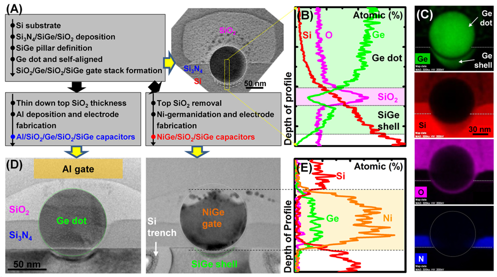
Figure 1. (A) Schematic of the nanofabrication process, TEM images, EDX elemental X-ray (B) line-scan spectra and (C) mapping micrographs for a SiO2/Ge-dot/SiO2/SiGe-shell MOS heterostructure on the Si substrate. (D) TEM cross-sections of an Al/SiO2/Ge-dot/SiO2/SiGe and a NiGe/SiO2/SiGe MOS capacitors with (E) corresponding EDX line-scan spectra confirming the complete Ni germanidation of the dot.
For MOS capacitors (Figure 1D), two different device configurations of Al/SiO2/Ge dot/SiO2/SiGe and NiGe/SiO2/SiGe were fabricated by mean of our self-organized fabrication process described above. Two metallization schemes for fabricating gate electrodes were employed for forming (a) Al gates and (b) NiGe gates, respectively. The former is achieved by a direct etch back of the newly formed SiO2 layer over the Ge dots to a resulting gate oxide thickness of 15 nm, followed by the deposition of Al. The latter heterostructure is formed by the complete removal of the newly formed SiO2 layer over the Ge dots, followed by the deposition of 60 nm Ni and subsequent rapid thermal annealing at 400°C for 1 min within a N2 ambient (Jaeger et al., 2007; Brunco et al., 2008b). The strong intensity of Ni X-ray fluorescence within the entire dot as evidenced from cross-sectional transmission electron microscopy-energy dispersive X-ray (CTEM-EDX) line-scan examinations confirms the complete Ni germanidation of the Ge dot, as shown in Figure 1E. Meanwhile, a Si trench structure adjacent to the SiGe shell was designed for minimizing parasitic capacitance, as indicated in Figure 1D. The final process step for both MOS configurations is the fabrication of the substrate electrode on the backside of the Si substrate, followed by forming gas (95% N2 and 5% H2) annealing for 30 min at 400°C. Detailed characterization of interfacial morphologies and structural properties for the Ge dot/SiO2 and the SiO2/SiGe shell was conducted using high-resolution CTEM, EDX spectroscopy, and Raman spectroscopy. The interfacial electrical properties for the NiGe/SiO2/SiGe and the Al/SiO2/Ge-dot/SiO2/SiGe MOS capacitors were determined using frequency-dependent capacitance–voltage (C-V) and current–voltage (I-V) measurements over a range of temperatures (300–77 K).
Results
Our previous results (Chien et al., 2011; Kuo et al., 2012; Wang et al., 2013; Chen et al., 2014; Lai et al., 2015) have shown that thermal oxidation performed on poly-Si0.85Ge0.15 nano-pillar structures preferentially converts the Si from the poly-Si0.85Ge0.15 to SiO2, leading to the formation of a single Ge dot within each oxidized nano-pillar through an unusual Ostwald Ripening process consolidating the segregated Ge nanocrystallites (Chien et al., 2011). Interestingly, excess thermal oxidation (or thermal annealing) of 15–65 min enables the as-formed Ge dot to penetrate the underlying, buffer Si3N4 layer, and ultimately form a 2–15-nm-thick Si1− xGex-shell layer (x > 0.5) with a “cup”-shape morphology near the top surface of the Si substrate when the Ge dot comes in close proximity to the Si substrate. Essentially, Ge atoms migrate from the dot to convert the top surface of the Si substrate to a thin Si1− xGex shell (Figure 1A). Additionally, the Ge dot also catalyzes the formation of an amorphous oxide layer between the dot and the SiGe shell by oxidizing Si interstitials released by the faster oxidizing SiGe shell on the substrate. In this way, a MOS heterostructure of Ge-dot/oxide/SiGe shell is created in a single step by having a conformal interfacial gate dielectric layer around the Ge dot but also itself conformal with the SiGe shell/Si substrate (Figure 1C). The chemical composition of this interfacial, gate dielectric layer is confirmed by an EDX line scan to be SiO2 instead of GeOx as evidenced by a sharp dip in the Ge X-ray fluorescence combined with a significant increase in the Si signal (Figure 1B). Thus, we have a thermally stable dielectric layer of SiO2 between the Ge dot and the SiGe shell. Simultaneously, we prevent interfacial defect issues observed in conventional Ge MOSFET structures. These defects include the loss of Ge due to miscibility in Si, the formation of electrically active dislocations, and associated point defects that are generated during the strain relaxation of the lattice mismatch between Ge and Si.
Extensive TEM observations reveal that following the thermal oxidation, 7.5–90-nm-diameter Ge dots can be controllably produced from 20 to 240-nm-diameter Si0.85Ge0.15 nano-pillars with a pillar height of 5–70 nm, as shown in Figures 2A,B. The Ge-dot size appears to have a strong dependence on the total Ge content within the original SiGe nano-pillar. That is, the generation of a smaller Ge dot is made possible by thermally oxidizing a smaller volume SiGe nano-pillar (Figure 2C). Figure 3A shows that the thickness of the interfacial SiO2 layer (Tox) between the Ge dot and the SiGe shell is almost constant at 3.9 ± 0.4 nm regardless of the nano-pillar (or dot) size. However, this interfacial SiO2 layer reduces to 3.6 ± 0.4 nm in thickness by decreasing the annealing temperature to 850°C and further shrinks to 3.1 ± 0.25 nm when a poly-Si underlying layer is employed, as shown in Figures 3B–D. It is observed in Figures 4A,B that the SiGe-shell thickness (Tshell) and the penetration depth (Ddot) for Ge dots into the Si substrate also have a strong dependence on the Ge-dot sizes. Thus, we show our ability to exercise good control of the Ge-dot size, the interfacial SiO2 thickness, and the SiGe-shell thickness in our MOS heterostructure, thereby providing a core building block for Ge-based MOS devices. Moreover, the clear lattice fringes observed in the high-resolution TEM micrographs and the sharp, lattice-plane spots in the SiGe selected area diffraction patterns (SADs) in Figure 4C confirms the excellent crystallinity of the SiGe shell. Detailed analysis of the SADs give the average lattice spacings of the {110}, {111}, and {311} SiGe planes as 3.928, 3.216, and 1.657 Å, corresponding to residual compressive strains of −1.60, −1, and −2.64%, respectively. Our previous work (Pezzoli et al., 2008; Liao et al., 2014) on the Raman characterization of the SiGe-shell region has also shown that Ge mole fractions as high as x = 0.55–0.72 are achieved for the SiGe shells formed from 50 to 90 nm Ge dots. The advantage of having single-crystalline Si1− xGex shells (x > 0.5) in a compressive stress state has extensive applications in nanoelectronics and nanophotonics, especially in SiGe (or Ge) p-MOS devices.
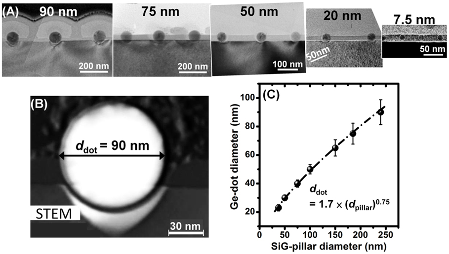
Figure 2. (A) TEM images for SiO2/Ge-dot/SiO2/SiGe-shell heterostructures containing 7.5–90-nm-diameter Ge dots, produced from 20 to 240-nm-diameter Si0.85Ge0.15 nano-pillars with pillar heights of 5–70 nm. (B) Representative scanning TEM micrograph of a 90-nm Ge dot and the corresponding gate-stack heterostructure. (C) The relationship of Ge-dot diameter (ddot) to the original SiGe nano-pillar diameter (dpillar) with a pillar height of 70 nm prior to the oxidation.
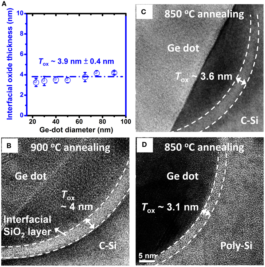
Figure 3. (A) The interfacial SiO2 layer has an almost constant 3.9-nm thickness regardless of the Ge-dot size. CTEM micrographs of the Ge-dot/SiO2 and SiO2/SiGe-shell interfaces for the proposed MOS structure fabricated on a Si substrate following thermal annealing at (B) 900°C and (C) 850°C. (D) The interfacial oxide thickness is smaller, i.e., ~3 nm for the case of our MOS structure nanofabricated over poly-Si and annealed at 850°C.
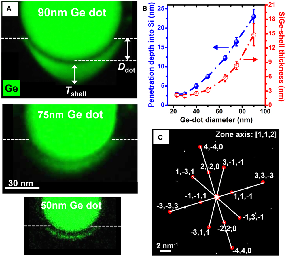
Figure 4. (A) EDX elemental X-ray mapping micrographs for the SiGe shells generated by 90, 75, and 50-nm-diameter Ge dots, respectively. (B) Penetration depth of the Ge dot into Si (Ddot) and SiGe-shell thickness (Tshell) as a function of the Ge-dot diameter. (C) Selected area diffraction pattern of a SiGe shell in (A) confirms its good crystallinity and its state of compressive strain.
Figure 5A shows the high-/low-frequency C–V characteristics of NiGe/SiO2/SiGe and Al-gate/SiO2/Ge-dot/SiO2 MOS capacitors measured at 77–300 K. Both devices exhibit good gate bias control of the surface charge and minority carriers at 100 Hz–1 MHz. The measured gate dielectric capacitances (Cox) in the accumulation region are 8–8.8 and 5–5.5 pF, respectively, for NiGe/SiO2/SiGe and Al-gate/SiO2/Ge-dot/SiO2 capacitors. These measurements are in reasonable agreement with the theoretically calculated values of ~8.7 and 5.9 pF based on the dielectric layer thicknesses, dielectric constants, and gate areas. From the extensive, variable temperature high-/low-frequency C–V characteristics, the extracted Dit values show a typical U-shaped distribution profile across the energy band gap with minimum Dit of ~4.5 × 10¹¹ and ~3 × 1011 cm−2⋅eV−1, respectively, for NiGe/SiO2/SiGe and Al-gate/SiO2/Ge-dot/SiO2 MOS capacitors, as shown in Figure 5B. A significantly large negative flat-band voltage (Vfb) is observed for both NiGe/SiO2/SiGe and Al-gate/SiO2/Ge-dot/SiO2 MOS capacitors, suggesting the presence of positive fixed charges. The measured interface trap densities and fixed charge densities are comparable to the reported values (1011–1012 cm−2) of state-of-the-art Ge MOS capacitors (Lee et al., 2011; Xie et al., 2012), suggesting that good-quality interface properties are achievable for our fabricated MOS gate-stack structures. Figure 5C contains the I–V characteristics of NiGe/SiO2/SiGe capacitors, showing the typical features of direct tunneling, Fowler–Nordheim tunneling, and hard breakdown, as indicated by regions I, II, and III, respectively. A low leakage current density of about 10−9 A/cm2 and a high breakdown electric field (E field) of 8.3 MV/cm further confirm the electrical robustness of the 3.9-nm-thick interfacial SiO2 layer.
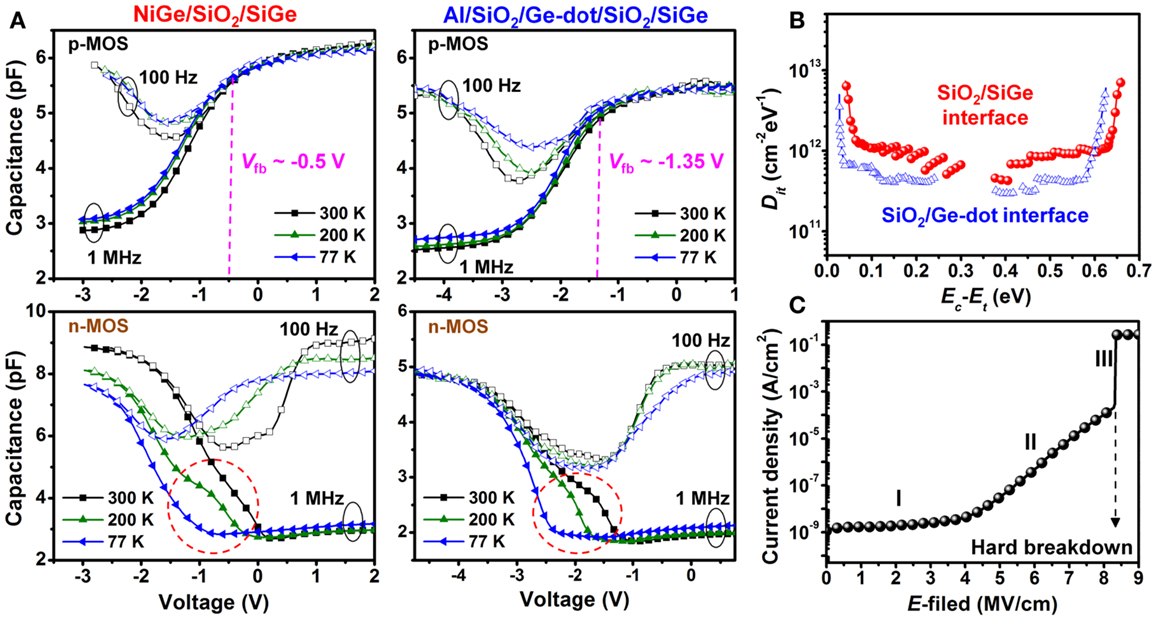
Figure 5. (A) Frequency-dependent C–V characteristics and (B) extracted Dit for NiGe/SiO2/SiGe and Al/SiO2/Ge-dot/SiO2/SiGe capacitors in the temperature range of 300–77 K. Red dashed circles indicate weak-inversion humps because of the faster capture and emission of carriers within the small bandgap of Ge. (C) I–V behavior of NiGe/SiO2/SiGe capacitors confirms the robustness and integrity of interfacial oxide layer.
Discussion
We have clearly demonstrated that our proposed MOS gate-stack structure is not only formed in a self-organized manner but also possesses excellent, process-controllable, size tunability. For Ge MOS transistor applications, the gate geometry or channel length (Lg) of the MOS structure is directly dependent on the diameter of the Ge dot (ddot). As mentioned above, ddot is essentially determined by the total Ge content within the original Si1− xGex nano-pillar and therefore, lithographically controllable via the geometrical dimensions (diameter: dpillar and height) and the composition of the original Si1− xGex nano-pillar prior to oxidation. For Si0.85Ge0.15 nano-pillars with a pillar height of 70 nm, the relationship between the experimentally produced Ge-dot size and the original Si0.85Ge0.15 nano-pillar diameter is well described by ddot = 1.7 × (dpillar)0.75 (Figure 2C), indicating good mass conservation of the Ge content prior to and following the thermal oxidation. This experimental fact demonstrates that as compared to the direct fabrication of nano-channels in bottom-up methods for conventional MOSFETs, our approach lends itself to simplified process control. Only the geometry of the original SiGe need be controlled in order to generate the desired MOS geometry via nano-patterning steps.
As regards the interfacial oxide layer separating the Ge dot and the SiGe shell/Si substrate, its thermal stability, gate oxide integrity, and thickness scalability determine the performance of our Ge MOS devices. Our previously reports (Kuo et al., 2012; Chen et al., 2014; Lai et al., 2015) have described that the interfacial SiO2 thickness is determined by an exquisitely controlled dynamic balance that exists between the fluxes of oxygen and Si interstitials. Thus, judicial control of either the source of Si interstitials or the flux of oxygen interstitials by changing thermal annealing conditions during the penetration of Ge dot effectively controls the interfacial SiO2 thickness. The shrinkage of the interfacial SiO2 layer in thickness is enabled by either decreasing the annealing temperature to 850°C or by employing a poly-Si underlying layer (Figures 3B–D), demonstrating, once again, that the interfacial layers within our MOS heterostructure are individually tunable. We believe that with further optimization of substrate and thermal annealing parameters, the interfacial SiO2 thickness could be made even smaller, i.e., below 1 nm, if needed for advanced Ge MOS applications. Additionally, the presence of a robust, thermally stable SiO2 interfacial layer completely obviates GeO desorption issues experienced by previous workers. As described previously, GeO desorption has a severe and detrimental impact on the Ge/dielectric interface and consequently the thermal stability of Ge MOS devices during sequential high-temperature processes (Toriumi et al., 2009; Lee et al., 2011). In contrast, our Ge-MOS oxide stability is evidenced by the abrupt interfacial boundaries and an absence of structural defects. Also, and importantly, such an amorphous SiO2 interfacial layer effectively decouples the lattice-mismatch constraints between the Ge dot and the Si substrate. The absence of lattice mismatch generated defects, such as dislocations and point defects, is particularly beneficial for the production of Ge-on-Si photonic devices. Hence, our MOS heterostructure and associated processing eliminate not only the stringent limitations on the thermal budget for processing conventional Ge MOS structures but also the complicated surface cleaning and interfacial treatments that are needed prior to and following the deposition of each layer within the conventional Ge MOS gate stack.
Good process control of the composition, thickness, and crystallinity of the SiGe channel is essential for the application of our Si1− xGex shell as a high-mobility channel material in nanoelectronics. Our SiGe shell is generated by the substitutional diffusion of Ge within the Si substrate. Thus, since the Ge dot is a sufficiently large source of Ge atoms, the thickness and chemical composition of the SiGe shell are mainly determined by the diffusion coefficient of Ge in Si, the oxidation temperature and time, and the Ge-dot size. Figures 4A,B do indeed show a strong dependence the SiGe-shell thickness on the Ge-dot size. The estimated diffusion lengths for Ge in Si at a temperature of 900°C and for diffusion times of 15–65 min are 1.5–2.4 nm, respectively, based on the diffusion coefficient equation of DGe in Si = 1.03 × 10⁵⋅exp(−5.33/kB T) (Fahey et al., 1989; Silvestri et al., 2006), where kB T represents the thermal energy, in our case, at 900°C. The theoretically calculated values are in reasonable agreement with the observed thicknesses of 2–3 nm for the SiGe shells formed from the 20–50 nm Ge dots, but they are too small to explain SiGe-shell thicknesses of 6–15 nm when the Ge dot increases to 50–90 nm in diameter. We have experimentally determined that the formation of substantially thicker SiGe shells is associated with these larger Ge dots catalytically enhancing the release of Si interstitials from the Si substrate. Therefore, for the case of larger Ge dots, interstitial generation significantly increases Si vacancy concentrations and consequently enhances Ge diffusion lengths. Increased catalytic generation of Si interstitials is also clearly evidenced by the enhanced penetration depth for Ge dots into the Si substrate with increasing the dot size, as shown in Figures 4A,B. In summary, the thicker Si1− xGex shells resulting from the larger Ge dots have shown us that Ge diffusion lengths in Si calculated using conventional formulas may have to be revised in light of the observed Ge-catalyzed Si vacancy enhancement. In addition to excellent crystallinity confirmed by the clear lattice fringes observed in the high-resolution TEM micrographs and SADs, our previous work (Liao et al., 2014) on the Raman characterization of the SiGe-shell region has shown a large blue shift of the longitudinal optical Ge–Ge phonon line (309 cm−1 from the SiGe shell as opposed to the 301 cm−1 for bulk Ge). This blue shift suggests the SiGe shell is being subjected to a compressive strain of ~1.6% and is therefore in reasonable agreement with the SAD analysis from Figure 4C. Also, the appearance of a weak Raman signal at 406–414 cm−1 suggests that the chemical composition of the Si1− xGex shell has a strong dependence on the dot size. The Ge mole fraction is as high as x = 0.55–0.72 for the SiGe shells formed from 50 to 90 nm Ge dots (Pezzoli et al., 2008; Liao et al., 2014).
As described above, the thickness of the SiGe shell is tunable simply by controlling the flux of Ge atoms leaving the dots to form the SiGe shells on the surface of the Si substrate. It is indeed interesting to note that a corresponding SiGe shell is not discernible on the surface of the Ge dot in spite of the fact that dissolution of Ge in Si actually requires a larger enthalpy (38.4 kJ/mole) than for Si to dissolve in Ge (30.7 kJ/mole) (Harrison and Kraut, 1988). The absence of the SiGe shell in the Ge dot could be attributable to the rapid migration of Si interstitials over the surface of the Ge dot enroute to their oxidation at the distal surface of the dot. Thus, even if Si is fully soluble in Ge, the chemical gradient created by the high temperature oxidation process acts as a “sink” for Si interstitials. Experimentally, we have shown that the Si X-ray fluorescence signal is undetectable within the Ge dots in Figures 1B,C.
A MOS capacitor is the basic, effective core device for qualifying the integrity of a novel gate-stack structure. In particular, the electrical properties of the interface between the inversion layer and gate dielectric layers can be exquisitely characterized using an MOS device. In our particular case, there are two interfaces of interest, namely the SiO2/Ge-dot and the SiO2/SiGe-shell interfaces. These interfaces are in series for our self-organized SiO2/Ge-dot/SiO2/SiGe heterostructure. In order to fully exploit the electrical interfacial properties of our MOS gate-stack heterostructures, we fabricated both NiGe-dot/SiO2/SiGe and Al/SiO2/Ge-dot/SiO2/SiGe MOS capacitors and then characterized the interfaces of the SiO2/SiGe shell and the SiO2/Ge dot, respectively, for both device types. Both MOS capacitors of the NiGe/SiO2/SiGe and the Al/SiO2/Ge-dot/SiO2/SiGe types feature interface trap densities of as low as 3–5 × 1011 cm−2⋅eV−1 (Figures 5A,B) and which are insensitive to the dot (nano-pillar) density and to the gate areas. The measured low Dit for NiGe/SiO2/SiGe MOS capacitors suggests excellent quality for the SiO2/SiGe-shell interface. Also, the comparably low Dit for Al/SiO2/Ge-dot/SiO2/SiGe MOS capacitors suggests that the SiO2/Ge-dot interface system is at least as good as the SiO2/SiGe-shell interface. The apparent weak-inversion humps induced in Al/SiO2/Ge-dot/SiO2/SiGe n-MOS devices at 300 K, and which are suppressed at 77 K, probably originate from the fast capture and emission of carriers within the small bandgap of Ge (Marten et al., 2008; Kobayashi et al., 2009; Swaminathan et al., 2010).
The Al/SiO2/Ge-dot/SiO2/SiGe heterostructures exhibit a larger negative Vfb than the corresponding NiGe-dot/SiO2/SiGe MOS capacitors, as shown in Figure 5A. Also, the measured Vfb is nearly independent of the dot size (20–90 nm) or the original nano-pillar diameter (30–240 nm). In theory, Vfb is primarily determined by the work function difference (φms) between the gate material and the semiconductor. Vfb values are modified by stored charges (fixed charge: Qf and interfacial charges: Qit) located at the gate oxide/semiconductor interface, i.e., Vfb = φms − (Qf + Qit)/Cox. Considering the work functions for Al (4.16 eV), NiGe (5.2 eV), Ge (4.33 eV), and SiGe (4.55 eV) and the gate oxide thickness of 3–4 nm, our experimental observations of negative Vfb suggest estimated positive fixed charge densities of ~5 × 1011 cm−2 at interfaces of SiO2/SiGe and SiO2/Ge dot. It is interesting to note that the positive fixed charges measured for our NiGe/SiO2/SiGe and Al/SiO2/Ge-dot/SiO2/SiGe MOS capacitors are in contrast to the conventional expectation of negative fixed charges produced by the thermal oxidation of SiGe alloys (LeGoues et al., 1989; Nayak et al., 1990, 1992) or at high-k dielectric/Ge interfaces generated either by chemical vapor deposition or atomic layer deposition (Bai et al., 2005; Zhang et al., 2006; Deng et al., 2011) As described in our previous reports (Kuo et al., 2012; Lai et al., 2015), the interfacial SiO2 layer between the Ge dot and the SiGe shell is formed by the thermal oxidation of Si interstitials that are released from the Si substrate. The oxide layer between the Ge dot and the deposited Al gate is formed by the thermal oxidation of Si interstitials that migrate along the surface of Ge dot to its distal end. We believe that the observed positive fixed charges and interface traps very likely originate from dangling bonds within the SiGe shell and from residual, unoxidized Si interstitials. To our knowledge, the experimentally measured interface trap densities and fixed charge densities in our self-organized Ge-dot/SiO2/SiGe gate-stack heterostructures are better, or at the very least, comparable to the reported values (1011–1012 cm−2) for Ge/GeO2 or Ge/GeO2/high-k MOS devices (Swaminathan et al., 2009; Lee et al., 2011; Nishimura et al., 2011; Xie et al., 2012; Zhang et al., 2012; Takenaka et al., 2013). In these cases, the Ge/GeO2 structures are subjected to the additional expense of special interfacial treatments prior to and following gate oxidation. The exploration of post-annealing processes for suppressing fixed charges and interface traps are the subject of ongoing research.
In conclusion, we report the first-of-its-kind, unique, CMOS-compatible approach for generating a self-aligned, gate-stacking MOS heterostructure of SiO2/Ge-dot/SiO2/Ge-shell over the Si substrate. Our MOS structures are nanofabricated in a single oxidation step of SiGe nano-pillars that are lithographically patterned over a buffer Si3N4 layer on the Si substrate. Process-controlled tunability of the Ge-dot size (20–90 nm), the SiO2 thickness (3–4 nm), and the SiGe-shell thickness (2–15 nm) have been demonstrated. Good interfacial and electrical properties with low Dit of 3–5 × 1011 cm−2⋅eV−1 and fixed charge densities of 1–5 × 1011 cm−2 are observed for SiO2/SiGe and SiO2/Ge interfaces, respectively, and are comparable to literature-reported values for state-of-the-art Ge MOS capacitors. In comparison to previously proposed Ge-based devices, our MOS heterostructure not only exhibits superior performance but also has simplicity and elegance in terms of its one-step fabrication process. Therefore, we envisage further scientific exploration of our MOS heterostructures toward the ultimate goal of demonstrating advanced Ge-based MOS nanoelectronic and nanophotonic devices.
Author Contributions
W-TL conceived the experimental work and contributed to data analysis and the manuscript preparation. K-CY performed structure/device fabrication and characterization. P-HL carried out the diffraction pattern and Raman examination and analysis. TG conceived the mechanism of heterostructure formation and revised the manuscript. P-WL conceived the study, revised the manuscript, and supervised the work. All authors read and approved the final manuscript.
Conflict of Interest Statement
The authors declare that the research was conducted in the absence of any commercial or financial relationships that could be construed as a potential conflict of interest.
Funding
This work was supported by the Ministry of Science and Technology of Republic of China (MOST 102-2221-E-009-195-MY3 and 104-2221-E-009-064) and by the Asian Office of Aero-space Research and Development under contract no. FA 2386-15-1-4025.
References
Assefa, S., Xia, F., Bedell, S. W., Zhang, Y., Topuria, T., Rice, P. M., et al. (2010). CMOS-integrated high-speed MSM germanium waveguide photodetector. Opt. Express 18, 4986–4999. doi: 10.1364/OE.18.004986
Bai, W. P., Lu, N., and Kwong, D.-L. (2005). Si interlayer passivation on germanium MOS capacitors with High-k dielectric and metal gate. IEEE Electron Device Lett. 26, 378–380. doi:10.1109/LED.2005.848128
Brunco, D. P., De Jaeger, B., Eneman, G., Mitard, J., Hellings, G., Satta, A., et al. (2008a). Germanium MOSFET devices: advances in materials understanding, process development, and electrical performance. J. Electrochem. Soc. 155, H552–H561. doi:10.1149/1.2919115
Brunco, D. P., Opsomer, K., Jaeger, B. D., Winderickx, G., Verheyden, K., and Meuris, M. (2008b). Observation and suppression of nickel germanide overgrowth on germanium substrates with patterned SiO2 structures. Electrochem. Solid State Lett. 11, H39–H41. doi:10.1149/1.2820441
Camacho-Aguilera, R. E., Cai, Y., Patel, N. J., Bessette, T., Romagnoli, M., Kimerling, L. C., et al. (2012). An electrically pumped germanium laser. Opt. Express 20, 11316–11320. doi:10.1364/OE.20.011316
Chaisakul, P., Marris-Morini, D., Rouifed, M. S., Isella, G., Chrastina, D., Frigerio, J., et al. (2012). 23 GHz Ge/SiGe multiple quantum well electro-absorption modulator. Opt. Express 20, 3219–3224. doi:10.1364/OE.20.003219
Chen, K. H., Wang, C. C., George, T., and Li, P. W. (2014). The role of Si interstitials in the migration and growth of Ge nanocrystallites under thermal annealing in an oxidizing ambient. Nanoscale Res. Lett. 9, 339. doi:10.1186/1556-276X-9-339
Chien, C. Y., Chang, Y. J., Chen, K. H., Lai, W. T., George, T., Scherer, A., et al. (2011). Nanoscale, catalytically enhanced local oxidation of silicon-containing layers by ‘burrowing’. Nanotechnology 22, 435602. doi:10.1088/0957-4484/22/43/435602
del Alamo, J. A. (2011). Nanometre-scale electronics with III–V compound semiconductors. Nature 479, 317–323. doi:10.1038/nature10677
del Alamo, J. A., Antoniadis, D., Guo, A., Kim, D. H., Kim, T. W., Lin, J., et al. (2013). “InGaAs MOSFETs for CMOS: recent advances in process technology,” in International Electron Devices Meeting (Washington, DC: IEEE), 2.1.1–2.1.4.
Deng, S., Xie, Q., Deduytsche, D., Schaekers, M., Lin, D., and Caymax, M. (2011). Effective reduction of fixed charge densities in germanium based metal-oxide-semiconductor devices. Appl. Phys. Lett. 99, 052906. doi:10.1063/1.3622649
Doornbos, G., and Passlack, M. (2010). Benchmarking of III–V n-MOSFET maturity and feasibility for future CMOS. IEEE Electron Device Lett. 31, 1110–1112. doi:10.1109/LED.2010.2063012
Fahey, P., Iyer, S. S., and Scilla, G. J. (1989). Experimental evidence of both interstitial – and vacancy-assisted diffusion of Ge in Si. Appl. Phys. Lett. 54, 843. doi:10.1063/1.100863
Feng, D., Liao, S., Liang, H., Fong, J., Bijlani, B., Shafiiha, R., et al. (2012). High speed GeSi electro-absorption modulator at 1550 nm wavelength on SOI waveguide. Opt. Express 20, 22224–22232. doi:10.1364/OE.20.022224
Going, R., Seok, T. J., Loo, J., Hsu, K., and Wu, M. C. (2015). Germanium wrap-around photodetectors on silicon photonics. Opt. Express 23, 11975–11984. doi:10.1364/OE.23.011975
Gu, J. J., Liu, Y. Q., Wu, Y. Q., Colby, R., Gordon, R. G., and Ye, P. D. (2011). “First experimental demonstration of gate-all-around III-V MOSFETs by top-down approach,” in International Electron Devices Meeting (Washington, DC: IEEE), 33.2.1–33.2.4.
Gupta, S., Chen, R., Magyari, K. B., Lin, H., Yang, B., Nainani, A., et al. (2011). “GeSn technology: extending the Ge electronics roadmap,” in International Electron Devices Meeting (Washington, DC: IEEE), 16.6.1–16.6.4.
Harrison, W. A., and Kraut, E. A. (1988). Energies of substitution and solution in semiconductors. Phys. Rev. B 37, 8244–8256. doi:10.1103/PhysRevB.37.8244
Haurylau, M., Chen, G., Chen, H., Nelson, N. A., Albonesi, D. H., Friedman, E. G., et al. (2007). On-chip optical interconnect roadmap: challenges and critical directions. IEEE J. Sel. Top. Quantum Electron. 12, 1699–1705. doi:10.1109/JSTQE.2006.880615
Heck, M. J. R., Chen, H. W., Fang, A. W., Koch, B. R., Liang, D., Park, H., et al. (2011). Hybrid silicon photonics for optical interconnects. IEEE J. Sel. Top. Quantum Electron 17, 333–346. doi:10.1109/JSTQE.2010.2051798
Heyns, M., and Tsai, W. (2009). Ultimate scaling of CMOS logic devices with Ge and III–V materials. MRS Bull. 34, 485–492. doi:10.1557/mrs2009.136
Jaeger, B. D., Kaczer, B., Zimmerman, P., Opsomer, K., Winderickx, G., Steenbergen, J. V., et al. (2007). Ge deep sub-micron HiK/MG pFETs with superior drive compared to Si HiK/MG state-of-the-art reference. Semicond. Sci. Technol. 22, S221–S226. doi:10.1088/0268-1242/22/1/S52
Kamata, Y. (2008). High-k/Ge MOSFETs for future nanoelectronics. Mater. Today 11, 30–38. doi:10.1016/S1369-7021(07)70350-4
Kobayashi, M., Thareja, G., Ishibashi, M., Sun, Y., Griffin, P., McVittie, J., et al. (2009). Radical oxidation of germanium for interface gate dielectric GeO2 formation in metal-insulator-semiconductor gate stack. J. Appl. Phys. 106, 104117. doi:10.1063/1.3259407
Kuo, M. H., Lai, W. T., Hsu, T. M., Chen, Y. C., Chang, C. W., Chang, W. H., et al. (2015). Designer germanium quantum dot phototransistor for near infrared optical detection and amplification. Nanotechnology 26, 055203. doi:10.1088/0957-4484/26/5/055203
Kuo, M. H., Wang, C. C., Lai, W. T., George, T., and Li, P. W. (2012). Designer Ge quantum dots on Si: a heterostructure configuration with enhanced optoelectronic performance. Appl. Phys. Lett. 101, 223107. doi:10.1063/1.4768292
Lai, W. T., Yang, K. C., Hsu, T. C., Liao, P. H., George, T., and Li, P. W. (2015). A unique approach to generate self-aligned SiO2/Ge/SiO2/SiGe gate-stacking heterostructures in a single fabrication step. Nanoscale Res. Lett. 10, 224. doi:10.1186/s11671-015-0927-y
Lee, C. H., Nishimura, T., Nagashio, K., Kita, K., and Toriumi, A. (2011). High-electron-mobility Ge/GeO2 n-MOSFETs with two-step oxidation. IEEE Trans. Electron Devices 58, 1295–1301. doi:10.1109/TED.2011.2111373
LeGoues, F. K., Rosenberg, R., Nguyen, T., Himpsel, F., and Meyerson, B. S. (1989). Oxidation studies of SiGe. J. Appl. Phys. 65, 1724. doi:10.1063/1.342945
Liao, P. H., Hsu, T. C., Chen, K. H., Cheng, T. H., Hsu, T. M., Wang, C. C., et al. (2014). Size-tunable strain engineering in Ge nanocrystals embedded within SiO2 and Si3N4. Appl. Phys. Lett. 105, 172106. doi:10.1063/1.4900942
Liu, J., Kimerling, L. C., and Michel, J. (2012). Monolithic Ge-on-Si lasers for large-scale electronic-photonic integration. Semicond. Sci. Technol. 27, 094006. doi:10.1088/0268-1242/27/9/094006
Liu, J., Sun, X., Camacho-Aguilera, R., Kimerling, L. C., and Michel, J. (2010). Ge-on-Si laser operating at room temperature. Opt. Lett. 35, 679–681. doi:10.1364/OL.35.000679
Liu, J. F., Ahn, D., Hong, C. Y., Pan, D., Jongthammanurak, S., Beals, M., et al. (2006). “Waveguide integrated Ge p-i-n photodetectors on a silicon-on-insulator platform,” in Optoelectronics, Optics Valley of China International Symposium (Wuhan: IEEE), 1–4.
Marten, K., Chui, C. O., Brammertz, G., Jaeger, B. D., Kuzum, D., Meuris, M., et al. (2008). On the correct extraction of interface trap density of MOS devices with high-mobility semiconductor substrates. IEEE Trans. Electron Devices 55, 547–556. doi:10.1109/TED.2007.912365
Nayak, D. K., Kamjoo, K., Park, J. S., Woo, J. C. S., and Wang, K. L. (1990). Wet oxidation of GeSi strained layers by rapid thermal processing. Appl. Phys. Lett. 57, 369. doi:10.1063/1.103694
Nayak, D. K., Kamjoo, K., Park, J. S., Woo, J. C. S., and Wang, K. L. (1992). Rapid isothermal processing of strained GeSi layers. IEEE Trans. Electron Devices 39, 56–62. doi:10.1109/16.108212
Nishimura, T., Lee, C. H., Tabata, T., Wang, S. K., Nagashio, K., Kita, K., et al. (2011). High-electron-mobility Ge n-channel metal-oxide-semiconductor field-effect transistors with high-pressure oxidized Y2O3. Appl. Phys. Express 4, 064201. doi:10.1143/APEX.4.064201
Oktyabrsky, S., Nishi, Y., Koveshnikov, S., Wang, W. E., Goel, N., and Tsai, W. (2010). Fundamentals of III-V Semiconductor MOSFETs. Boston: Springer.
Pezzoli, F., Bonera, E., Grilli, E., Guzzi, M., Sanguinetti, S., Chrastina, D., et al. (2008). Raman spectroscopy determination of composition and strain in Si1-xGex/Si heterostructures. Mater. Sci. Semicond. Proc. 11, 279–284. doi:10.1016/j.mssp.2008.09.012
Ren, S., Rong, Y., Claussen, S. A., Schaevitz, R. K., Kamins, T. I., Harris, J. S., et al. (2012). Ge/SiGe quantum well waveguide modulator monolithically integrated with SOI waveguides. IEEE Photon. Technol. Lett. 24, 461–463. doi:10.1109/LPT.2011.2181496
Silvestri, H. H., Bracht, H., Hansen, J. L., Larsen, A. N., and Haller, E. E. (2006). Diffusion of silicon in crystalline germanium. Semicond. Sci. Technol. 21, 758–762. doi:10.1088/0268-1242/21/6/008
Sorianello, V., De Angelis, G., De Iacovo, A., Colace, L., Faralli, S., and Romagnoli, M. (2015). High responsivity SiGe heterojunction phototransistor on silicon photonics platform. Opt. Express 23, 28163–28169. doi:10.1364/OE.23.028163
Swaminathan, S., Oshima, Y., Kelly, M. A., and McIntyre, P. C. (2009). Oxidant prepulsing of Ge (100) prior to atomic layer deposition of Al2O3: in situ surface characterization. Appl. Phys. Lett. 95, 032907. doi:10.1063/1.3177195
Swaminathan, S., Shandalov, M., Oshima, Y., and McIntyre, P. C. (2010). Bilayer metal oxide gate insulators for scaled Ge-channel metal-oxide-semiconductor devices. Appl. Phys. Lett. 96, 082904. doi:10.1063/1.3313946
Takenaka, M., Zhang, R., and Takagi, S. (2013). “MOS interface engineering for high-mobility Ge CMOS,” in IEEE International Reliability Physics Symposium (Anaheim, CA: IEEE), 1–4.
Toriumi, A., Tabata, T., Lee, C. H., Nishimura, T., Kita, K., and Nagashio, K. (2009). Opportunities and challenges for Ge CMOS – control of interfacing field on Ge is a key. Microelectron. Eng. 86, 1571–1576. doi:10.1016/j.mee.2009.03.052
Vlasov, Y. A. (2015). “Silicon integrated nanophotonics: from fundamental science to manufacturable technology,” in Proceedings of SPIE 9367, Silicon Photonics X, 93671X. San Francisco, CA.
Wang, C. C., Liao, P. H., Kuo, M. H., George, T., and Li, P. W. (2013). The curious case of exploding quantum dots: anomalous migration and growth behaviors of Ge under Si oxidation. Nanoscale Res. Lett. 8, 192. doi:10.1186/1556-276X-8-192
Wang, J., Yu, M., Lo, G., Kwong, D. L., and Lee, S. (2011). Silicon waveguide integrated germanium JFET photodetector with improved speed performance. IEEE Photon. Technol. Lett. 23, 765–767. doi:10.1109/LPT.2011.2132794
Wu, J. H., and Li, P. W. (2007). Ge nanocrystal metal-oxide-semiconductor transistors with Ge nanocrystals formed by thermal oxidation of poly-Si0.88Ge0.12. Semicond. Sci. Technol. 22, S89–S92. doi:10.1088/0268-1242/22/1/S21
Xie, Q., Deng, S., Schaekers, M., Lin, D., Caymax, M., Delabie, A., et al. (2012). Germanium surface passivation and atomic layer deposition of high-k dielectrics – a tutorial review on Ge-based MOS capacitors. Semicond. Sci. Technol. 27, 074012. doi:10.1088/0268-1242/27/7/074012
Yu, H. Y., Ishibashi, M., Park, J. H., Kobayashi, M., and Saraswat, K. C. (2009). p-channel Ge MOSFET by selectively heteroepitaxially grown Ge on Si. IEEE Electron Device Lett. 30, 675–677. doi:10.1109/LED.2009.2019847
Zhang, Q., Huang, J., Wu, N., Chen, G., Hong, M., Bera, L. K., et al. (2006). Drive-current enhancement in Ge n-channel MOSFET using laser annealing for source/drain activation. IEEE Electron Device Lett. 27, 728–730. doi:10.1109/LED.2006.880655
Keywords: gate-stack, SiGe, self-organized, Ge dot, interface, size-tunable, MOS
Citation: Lai W-T, Yang K-C, Liao P-H, George T and Li P-W (2016) Gate-Stack Engineering for Self-Organized Ge-dot/SiO2/SiGe-Shell MOS Capacitors. Front. Mater. 3:5. doi: 10.3389/fmats.2016.00005
Received: 01 December 2015; Accepted: 25 January 2016;
Published: 11 February 2016
Edited by:
Salvatore Cosentino, University of Catania, ItalyReviewed by:
Steve Suib, The University of Connecticut, USAShinichi Saito, University of Southampton, UK
Copyright: © 2016 Lai, Yang, Liao, George and Li. This is an open-access article distributed under the terms of the Creative Commons Attribution License (CC BY). The use, distribution or reproduction in other forums is permitted, provided the original author(s) or licensor are credited and that the original publication in this journal is cited, in accordance with accepted academic practice. No use, distribution or reproduction is permitted which does not comply with these terms.
*Correspondence: Pei-Wen Li, pwli@nctu.edu.tw