Si/SiGe Heterointerfaces in One-, Two-, and Three-Dimensional Nanostructures: Their Impact on SiGe Light Emission
 David J. Lockwood
 Xiaohua Wu
 Jean-Marc Baribeau2
 Xiaolu Wang
 Leonid Tsybeskov
- 1Measurement Science and Standards, National Research Council, Ottawa, ON, Canada
- 2Information and Communications Technologies, National Research Council, Ottawa, ON, Canada
- 3Department of Electrical and Computer Engineering, New Jersey Institute of Technology, Newark, NJ, USA
Fast optical interconnects together with an associated light emitter that are both compatible with conventional Si-based complementary metal-oxide-semiconductor (CMOS) integrated circuit technology is an unavoidable requirement for the next-generation microprocessors and computers. Self-assembled Si/Si1−xGex nanostructures (NSs), which can emit light at wavelengths within the important optical communication wavelength range of 1.3–1.55 μm, are already compatible with standard CMOS practices. However, the expected long carrier radiative lifetimes observed to date in Si and Si/Si1−xGex NSs have prevented the attainment of efficient light-emitting devices, including the desired lasers. Thus, the engineering of Si/Si1−xGex heterostructures having a controlled composition and sharp interfaces is crucial for producing the requisite fast and efficient photoluminescence (PL) at energies in the range of 0.8–0.9 eV. In this paper, we assess how the nature of the interfaces between SiGe NSs and Si in heterostructures strongly affects carrier mobility and recombination for physical confinement in three dimensions (corresponding to the case of quantum dots), two dimensions (corresponding to quantum wires), and one dimension (corresponding to quantum wells). The interface sharpness is influenced by many factors, such as growth conditions, strain, and thermal processing, which in practice can make it difficult to attain the ideal structures required. This is certainly the case for NS confinement in one dimension. However, we demonstrate that axial Si/Ge nanowire (NW) heterojunctions (HJs) with a Si/Ge NW diameter in the range 50–120 nm produce a clear PL signal associated with band-to-band electron–hole recombination at the NW HJ that is attributed to a specific interfacial SiGe alloy composition. For three-dimensional confinement, the experiments outlined here show that two quite different Si1−xGex NSs incorporated into a Si0.6Ge0.4 wavy superlattice structure display PL of high intensity while exhibiting a characteristic decay time that is up to 1000 times shorter than that found in conventional Si/SiGe NSs. The non-exponential PL decay found experimentally in Si/SiGe NSs can be interpreted as resulting from variations in the separation distance between electrons and holes at the Si/SiGe heterointerface. The results demonstrate that a sharp Si/SiGe heterointerface acts to reduce the carrier radiative recombination lifetime and increase the PL quantum efficiency, which makes these SiGe NSs favorable candidates for future light-emitting device applications in CMOS technology.
Introduction
The group IV semiconductors silicon and germanium continue to be important materials for optoelectronic and electronic applications (Mangolini, 2013; Ray et al., 2013; Pavesi and Lockwood, 2016). Silicon, which has an indirect band gap of 1.1 eV, is used extensively in the microelectronics industry partly because of the stability of its oxide and this has allowed the development of reliable devices with nanoscale dimensions (Zwanenburg et al., 2013) even though the precise nature of the silicon–silicon oxide interface, even after decades of research, is still not completely understood (Omura et al., 2013). Germanium has a room temperature direct bandgap of 0.8 eV (~1.55 μm), and it is separated by only 0.14 eV from the indirect band gap of 0.66 eV. These properties make Ge one of the most promising materials for complementary metal-oxide-semiconductor (CMOS) compatible photonic components, including near-infra-red photodetectors (Ahn et al., 2007; Yin et al., 2007; Assefa et al., 2010; Michel et al., 2010) and, possibly, lasers (Liu et al., 2009, 2010; Camacho-Aguilera et al., 2012; Grydlik et al., 2016) in the desired wavelength region of 1.3–1.6 μm. However, it is well known that conventional Ge hetero-epitaxy on Si is complicated by the 4.2% difference in Ge and Si lattice constants (Paul, 2004; Shiraki and Sakai, 2005). Various techniques for building quality Si/Ge planar heterojunctions (HJs) include multi-step annealing to relax Ge layers and reduce the density of strain-induced dislocations (Saraswat et al., 2006; Ye and Yu, 2014), growth of ultra-thin Ge films and superlattices using Si1−xGex alloy transition layers with graded Ge composition x (Iyer et al., 1989; Nayak et al., 1996; Paul, 2004; Saraswat et al., 2006; Shah et al., 2010) and, alternatively, employ three-dimensional (3D) growth in the form of SiGe clusters and cluster multilayers using the Stranski–Krastanov (S-K) growth mode (Mo et al., 1990; Schmidt et al., 1999a; Shin et al., 2000; Baribeau et al., 2006). Another promising approach is to use one-dimensional (1D) growth in the form of nanowires (NWs) produced by the vapor–liquid–solid (VLS) growth mode or similar techniques (Wagner, 1970; Kamins et al., 2004; Hannon et al., 2006; Zakharov et al., 2006). With regard to interfacial properties, it should be noted that axial Si/Ge NW HJs, where the heterointerface is perpendicular to the NW axis, have a reduced heterointerface area compared to radial or “core-shell” NW HJs, where the Si/Ge heterointerface is parallel to the NW axis (Lauhon et al., 2002; Xiang et al., 2006; Zakharov et al., 2006).
In such applications, one of the defining parameters affecting the application of a Si or Ge nanostructure (NS) is, thus, its interfacial structure with its surroundings. The introduction of an interface modifies bulk material parameters (Barbagiovanni et al., 2012, 2014) and introduces new phenomena. Dangling bonds, stress, and defect states elicit the degree to which the interface potential confines charge carriers (Barbagiovanni et al., 2014). Any termination with atomic impurities, such as hydrogen or oxygen, at the interface influences the oscillator strength (Guerra and Ossicini, 2010) and creates polarization effects at the interface (Guerra et al., 2011). Sub-oxide interface states give rise to defect-induced carrier recombination effects that can dominate quantum confinement (QC) effects (Barbagiovanni et al., 2014, 2015). However, with careful control over the fabrication conditions (Lockwood et al., 2013a) and with appropriate interface characterization (Cosentino et al., 2014), Ge NSs can be produced that clearly exhibit QC effects (Barbagiovanni et al., 2015).
The development of a Si-based light emitter compatible with CMOS integrated circuit technology and the desired fast optical interconnects is essential for the upcoming generation of high-speed microprocessors and computers. Self-assembled Si/Si1−xGex NSs that can emit light in the optical communication wavelength range of 1.3–1.55 μm are presently well suited for use in CMOS foundries. However, the long carrier radiative lifetimes observed in such Si/Si1−xGex NSs hinder the development of efficient light-emitting devices and, thereby, the construction of lasers (Sturm et al., 1991; Zheng et al., 1994; Lu et al., 1995; Lockwood, 1998; Pavesi et al., 2000; Tsybeskov and Lockwood, 2009). The usual model for radiative recombination in Si/Si1−xGex NSs is based on a type II heterointerface energy band alignment (see Figure 1) (Kamenev et al., 2006; Mala et al., 2013). In type II band alignment, the electrons and holes are spatially separated, with in this case the electrons localized in Si and the holes located in the SiGe NS, which explains the experimentally observed long lifetime of the photoluminescence (PL) in Si/SiGe NSs (Kamenev et al., 2005, 2006; Tsybeskov and Lockwood, 2009; Mala et al., 2013). The SiGe NS PL saturates quickly, as the slow radiative recombination cannot compete with the faster Auger recombination even for modest carrier concentrations (Kamenev et al., 2005, 2006; Tsybeskov and Lockwood, 2009; Mala et al., 2013). For these reasons, it is necessary to produce Si/Si1−xGex heterostructures with good control over their composition and interface abruptness to enable the production of the sought after fast and efficient PL at 0.8–0.9 eV.
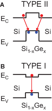
Figure 1. Schematic representation of (A) type II and (B) type I energy band alignments thought to exist in Si/Si1-xGex nanostructures. EC and EV are the energies of the conduction and valence bands, respectively, in Si and Si1−xGex.
A review of the light-emitting properties of SiGe NSs in general, including quantum wells (QWs), wires, and dots, has been given elsewhere (Lockwood and Tsybeskov, 2013). In this paper, which also summarizes some older work, we assess how the nature of the interfaces between SiGe NSs and Si in heterostructures strongly affects carrier mobility and recombination for physical confinement in one-, two-, or three-dimensions corresponding to the cases of QWs, quantum wires, and quantum dots, respectively.
Quantum Wells
The planar epitaxial growth of 100% Ge on Si is made difficult by their 4% lattice mismatch (Paul, 2004). However, the formation of structural defects, such as dislocations, which can give rise to a large number of undesirable non-radiative recombination centers, can be circumvented by the use of controlled-composition Si1−xGex alloys with 0.1 < x < 0.2, which can be grown with techniques, such as molecular beam epitaxy (MBE) or ultra-high vacuum (UHV) chemical vapor deposition (CVD). The resulting heterostructures display a low defect density at the Si/SiGe interfaces. Such Si/Si1−xGex multilayer NSs with 0.1 < x < 0.2 have been intensively studied in the past as a likely method to confine electron–hole pairs in double HJ, or QW, configurations and to reduce the thermal quenching of the luminescence at higher temperatures. So far, intense luminescence has been observed only at low temperatures in Si1−xGex in single and multiple QWs for x ≤ 0.2 [see Robbins et al. (1992)]. There have been several studies of the energy band alignment (i.e., to determine whether it is type I or type II; see Figure 1) in these NSs, but no final conclusions have yet been reached (Houghton et al., 1995; Thewalt et al., 1997; Shiraki and Sakai, 2005). Si and Ge interdiffusion during the growth of Si/Si1−xGex QWs broadens the heterointerfaces, but this interdiffusion can be reduced by using moderately low growth temperatures (less than 550°C). However, it should be noted that SiGe epitaxial growth at temperatures below 500°C usually produces a significantly high density of undesirable dislocations (Baribeau et al., 1990; Savage et al., 1999; Shiraki and Sakai, 2005). By staying within this fairly narrow growth “window,” high-quality Si/Si1−xGex QWs with x < 0.2 can be produced. Nevertheless, the thermal quenching of the PL quantum efficiency remains an unresolved problem in such QWs for the production of useful light emitters at wavelengths in the range of 1.3–1.5 μm.
Band Structure Engineering Via Brillouin Zone Folding in Atomic Layer Superlattices
Gnutzman and Clausecker (1974) postulated that Brillouin zone folding within superlattices where the individual layer thicknesses were multiples of the Si or Ge unit cell dimensions would create a new artificial unit cell along the growth direction that could result in the formation of a direct band gap material. Subsequently, high-quality (SimGen)p atomic layer superlattices, where m and n are the number of monolayers of Si and Ge, respectively, in each superlattice period and p is the number of periods, were grown in the 1980s by MBE (Kasper and Schäffler, 1991), which stimulated further this idea. The theoretical aspects were reconsidered by Jackson and People (1986) in 1986 and, thereafter, by other investigators. The essence of the zone-folding concept is demonstrated in Figure 2, where it can be seen that the new superlattice periodicity (d) creates a smaller Brillouin zone extending to ±π/d in contrast to that of the original material, which extends to ±2π/a where a is the lattice constant. The superlattice electronic band structure is then simply obtained by folding back the original band structure into this new reduced Brillouin zone. It is apparent from Figure 2 that for bulk Si the minimum in the conduction band, and thus a direct gap, can be obtained at the Brillouin zone center for d = 5a/2, which corresponds to 10 monolayers of Si. Given that the zone folding occurs only along the superlattice growth direction and that strains will appear to varying extents within the SimGen superlattice layers, together with modifications to the band offsets at the heterointerfaces, this somewhat naive picture will be modified [see, for example, Kasper and Schäffler (1991), Brey and Tejedor (1987), Froyen et al. (1987), Hybertsen and Schlüter (1987), and People and Jackson (1987)]. Theoretical work has shown that for strained layers of Si and appropriate superlattice periods a direct energy gap can be expected in these SimGen superlattices, but the calculated optical transition probability is still well below that of GaAs as the band-edge electronic states are inappropriately modified by the zone folding. Thus, the expected direct gap obtained by zone folding is now termed a quasi-direct band gap.
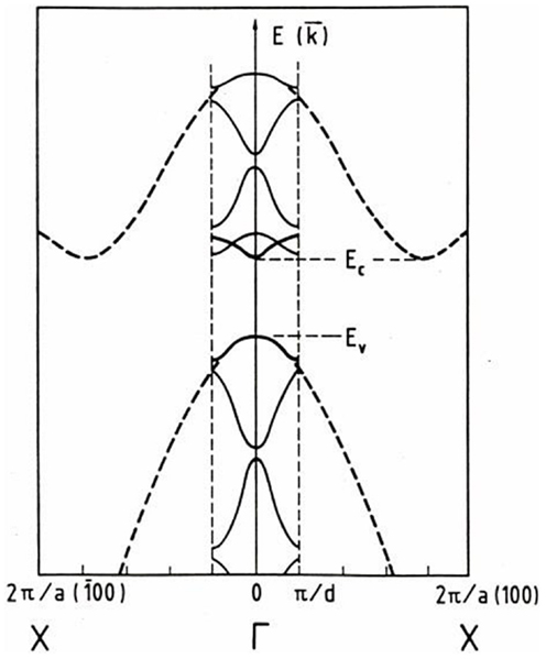
Figure 2. Schematic representation of the Brillouin zone-folding concept in Si resulting from the new superlattice periodicity in the growth direction. Here, the conduction band minimum along the X direction is folded back into the Г point when the superlattice period is about 10 monolayers of Si (Kasper and Schäffler, 1991).
Electroreflectance measurements of Si4Ge4 superlattices grown on (001)-oriented Si substrates (Pearsall et al., 1987) provided the first experimental evidence of the anticipated modifications to the Si and Ge band structures in such superlattices. It was not until later, when strain-symmetrized SimGen superlattices were first grown on strain-relaxed thick Si1−xGex alloy buffer layers on Si, that indications of the expected enhancement of the PL intensity and a smaller energy gap were obtained (Zachai et al., 1990; Kasper and Schäffler, 1991). Further improvements in the crystal growth conditions led to a positive identification of both of these novel features (Menczigar et al., 1993). Additional information on the research work on both the modified band structure and light emission in SimGen atomic layer structures is provided in the extensive review by Abstreiter (1998).
At low temperatures, infrared light emission at energies useful for fiber-optic transmission can easily be obtained from such SimGen superlattices. However, both the PL and the electroluminescence (EL) from such structures is basically quenched at room temperature primarily due to dissociation of the excitons and subsequent recombination of carriers at heterointerfaces or defects (Menczigar et al., 1992; Presting et al., 1992a). EL structures operating at room temperature have been reported (Engvall et al., 1993, 1995), but all the same, the infrared light emission is still quite weak. Results obtained more recently for a p-i-n diode based on a Si/Ge wavy superlattice quote an internal quantum efficiency of just ~10−5 at 300 K (Vescan and Stoica, 1998). Hence, it was thought that light sources based on the zone-folding concept were unlikely to produce useful devices. It was predicted that these atomic layer superlattices would be more likely to find ultimate use as infrared detectors instead of as light emitters (Presting et al., 1992b; Pearsall, 1994).
Part of the difficulty in reproducing the theoretical structures arises from the practical problem of producing the atomically abrupt interfaces required in these heterostructures. There have been considerable efforts made in trying to grow such atomically abrupt layered structures, but even with the best attempts using MBE there have been problems, such as atomic diffusion across interfaces (Lockwood et al., 1993), interface undulations (Lu et al., 1994), and surface segregation (Baribeau et al., 1996) that even after two decades of research have not been fully overcome.
Band Structure Engineering Via Alloying
Alloying Si with Ge and/or C also permits electronic band structure engineering, where the energy gap may be varied in this case by altering the alloy composition and/or strain (People and Jackson, 1990; Pearsall, 1994). When designing such heterostructures, the Si1−xGex layer thickness must be kept below the critical thickness, which is defined as the maximum thickness for defect-free strained growth of the layer. This implies that layers having larger thicknesses exhibit partial or total relaxation of the layer together with the formation of lattice defects, such as dislocations. The Si1−xGex critical thickness drops rapidly with increasing Ge concentration (Pearsall, 1994) and, hence, the emitting/absorbing regions in infrared emitters/detectors are necessarily quite thin. However, it is possible that wavy Si1−xGex/Si superlattice structures, which deviate from planar growth (see below), may alleviate this restriction (Baribeau et al., 1999). Moreover, and most significantly, it has been found that the alloy band gap remains indirect. These conditions place severe limits on the device structure. Nonetheless, considerable research has been undertaken on determining the optical properties of Si/Si1−xGex heterostructures (Pearsall, 1994), which exhibit type I band alignment (People and Jackson, 1990; Houghton et al., 1995) (see Figure 1), and, to a lesser extent, on Si/Si1−xCx or even Si/Si1−x−yGex Cy (St Amour et al., 1995; Orner et al., 1996; Soref et al., 1996; Sturm, 1998).
Photoluminescence and EL have both been detected from Si1−xGex alloy layers produced in both single epilayer and superlattice form with a higher intensity than that observed from bulk Si. The alloy layer luminescence energy exhibits the same dependence on x as the bulk energy gap, but it is at an overall lower energy (Noël et al., 1990; Rowell et al., 1990; Sturm et al., 1991; Lenchyshyn et al., 1992). The recombination mechanism can vary depending on the alloy layer thickness, its crystalline quality, and the heterointerface sharpness and can give rise to near band-edge light emission and/or excitonic luminescence (Noël et al., 1992; Lenchyshyn et al., 1993; Rowell et al., 1993). In early work, it was found that the EL from Si1−xGex/Si p-i-n diodes was quenched when the temperature was increased above 80 K (Rowell et al., 1990), but EL was later reported at higher temperatures (up to 220 K) in p-i-n diode structures (Robbins et al., 1991). There has been a continual improvement in materials quality and this, coupled with changes in device design, has continued to advance EL device performance [see, for example, Fukatsu et al. (1992), Mi et al. (1992), Kato et al. (1995), Förster et al. (1996), and Presting et al. (1996)] to the point that EL has been obtained at wavelengths near 1.3 μm at room temperature (Mi et al., 1992; Presting et al., 1996). From a practical point of view, one major problem with such devices at present is their low efficiency at room temperature, which results from thermal dissociation of the exciton (Mi et al., 1992; Presting et al., 1996). For example, Si1−xGex/Si p-i-n diodes that had been grown on patterned substrates to optimize the unrelaxed alloy layer thickness (Stoica et al., 1998) had an EL internal quantum efficiency of only ~10−4 at 300 K (Vescan and Stoica, 1998). Again, as for SimGen heterostructures, interface sharpness, or more-pointedly a lack thereof, is a critical factor in the diode performance.
Quantum Wires
Another remarkable option is to use NWs, which can be produced by VLS 1D growth or similar techniques (Wagner, 1970; Kamins et al., 2004; Hannon et al., 2006; Zakharov et al., 2006). Compared to 2D and 3D growth of NSs, NWs can form Si/Ge HJs having different geometries (e.g., axial Si/Ge NW HJs, where the Si/Ge heterointerfaces are perpendicular to the NW axes, and radial “core-shell” NW HJs, where the Si/Ge heterointerfaces are parallel to the NW axes) and locations (e.g., Ge NW-Si substrate HJs) (Lauhon et al., 2002; Xiang et al., 2006; Zakharov et al., 2006).
Since Ge has a larger lattice constant (5.658 Å) compared to Si (5.431 Å), it has been proposed that for axial Si/Ge NW HJs the strain created through the 4% lattice mismatch between Si and Ge can be relieved in part at the heterointerfaces via the lateral expansion of the Ge segment of the NW (Kästner and Gösele, 2004; Ertekin et al., 2005). Thus, investigations of axial Si/Ge NW HJs can open new and interesting prospects for constructing low defect-density NSs for applications in CMOS compatible photonic components. We have investigated such axial structures and summarize our findings below (Wang et al., 2015).
Nanowire Heterojunctions
For this study, axial Si/Ge NW HJs were grown using the VLS technique and Au nanoparticles as a precursor in a lamp-heated reduced-pressure CVD reactor (Chang et al., 2009). The samples were characterized with a transmission electron microscope (TEM) equipped with a field emission source and an energy-dispersive X-ray spectrometer (EDX) with a probe size of 0.2 nm, Raman scattering spectroscopy, and PL spectroscopy.
Figure 3 shows a TEM image at moderate resolution of a single axial Si/Ge NW HJ with a clearly visible Si/Ge heterointerface and smooth NW surface. The diameter of the Si segment of the NW is ~105 nm and it is nearly constant. The Ge segment of the NW diameter gradually increases from ~105 to 115 nm within ~100 nm from the Si/Ge heterointerface and then remains constant. Figure 4 presents a high-resolution TEM image of the Si/Ge NW heterointerface close to the NW center. A lattice fringe spacing fast Fourier transform (FFT) of the central heterointerface area indicated a nearly ideal crystallinity of the NW center. Figure 5 shows a TEM micrograph at high resolution of the same Si/Ge NW HJ with attention on the area close to the NW surface where a ~1-nm-thick amorphous oxide layer can be seen (marked by an arrow) and structural imperfections (see area marked by a box) are confirmed by a FFT analysis. No other structural defects are observed in the vicinity of the Si/Ge NW HJ.
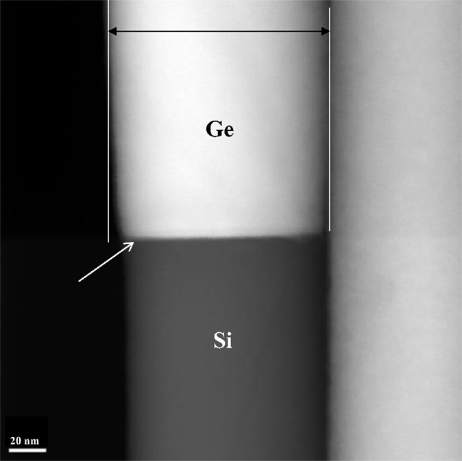
Figure 3. Transmission electron microscope (TEM) image of the axial Si/Ge nanowire (NW) heterojunction (HJ) showing an abrupt Si/Ge heterointerface (marked by the arrow) and an increase in the NW diameter from 105 nm in the Si segment to 115 nm in the Ge segment of the NW (Wang et al., 2015).
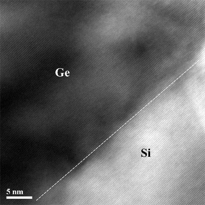
Figure 4. High-resolution TEM image of the Si/Ge NW HJ interface close to the NW center with clearly visible (111) lattice fringes (Wang et al., 2015).
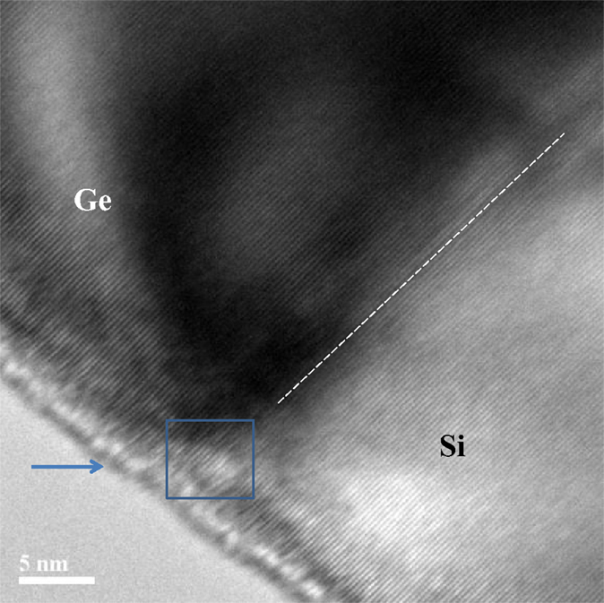
Figure 5. High-resolution TEM image of the Si/Ge NW HJ interface close to the NW surface with clearly observed distortion of the lattice fringes (see box). An amorphous layer of ~ 1 nm thickness at the NW surface is indicated by an arrow (Wang et al., 2015).
Results of compositional EDX microanalysis of the Si/Ge NW HJs are shown in Figure 6. The Si/Ge NW HJ is comprised of Si and Ge NW segments with a clearly observed ~8-nm-thick SiGe transition layer produced by spontaneous SiGe intermixing. The EDX data indicate that a 2-nm-thick Si0.8Ge0.2 layer is formed close to the Si segment of the NW, and this is known to be a stable SiGe alloy composition produced by spontaneous intermixing (Brunner, 2002; Kamenev et al., 2004).
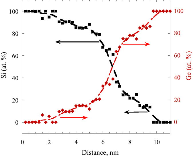
Figure 6. Compositional analysis of the NW along the growth direction showing a spontaneously formed SiGe transition alloy layer at the SiGe interface (Wang et al., 2015).
Figure 7A shows Raman spectra of Si/Ge NW HJs measured using lasers with different wavelengths. Under 515 nm excitation, we observe three distinct Raman peaks associated with the Si–Si (~520 cm−1), Si–Ge (~400 cm−1), and Ge–Ge (~300 cm−1) types of vibrations with the main Raman peak at 300 cm−1. Under 458 nm excitation, we observe the same peaks but with the main Raman peak now at ~520 cm−1. This difference is due to a strong spectral dependence of the Raman scattering cross-section (Cerdeira et al., 1972). A Raman peak at ~500 cm−1 is better observed using 458 nm excitation and is associated with the Si–Si vibration in the presence of a neighboring Ge atom denoted as Si–Si(Ge) (Alonso and Winer, 1989). The Raman spectra are also sensitive to the excitation intensity (see Figure 7B). As the excitation intensity increases, the major Raman peak at ~520 cm−1 broadens and shifts toward lower wavenumbers (similar behavior is observed for the Si–Ge and Ge–Ge Raman peaks, not shown). However, with increasing excitation intensity the Raman peak at 500 cm−1 shifts in the opposite direction.
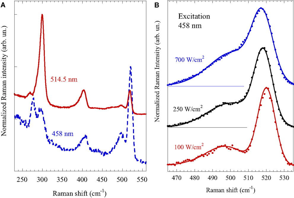
Figure 7. (A) Raman spectra of Si/Ge NW HJs obtained under different (indicated) excitation wavelengths. (B) Background-corrected Raman spectra obtained under 458 nm wavelength excitation and different (indicated) excitation intensities (Wang et al., 2015). Note that the second Raman peak around 270 cm−1 under 458 nm excitation is, most likely, associated with a laser plasma line.
Figure 8A shows the Si/Ge NW PL spectrum measured at low temperature. The PL spectrum clearly reveals at least two peaks: a narrower PL peak at ~1.08 eV (PL1) and a broader PL peak at ~1.03 eV (PL2). No significant PL at photon energies close to the bulk c-Si transverse optical (TO) phonon-replica PL peak at ~1.1 eV is found. The spectral positions and relative intensities of these two PL peaks are found to be temperature dependent (see Figure 8B): both PL peaks change their positions significantly with temperature and exhibit the lowest photon energy at ~60 K. The PL1 peak is detectable even at room temperature and exhibits an asymmetric broadening, which [in agreement with Tsybeskov et al. (1996)] can be fitted by employing Boltzmann thermal broadening on the high energy side of this feature.
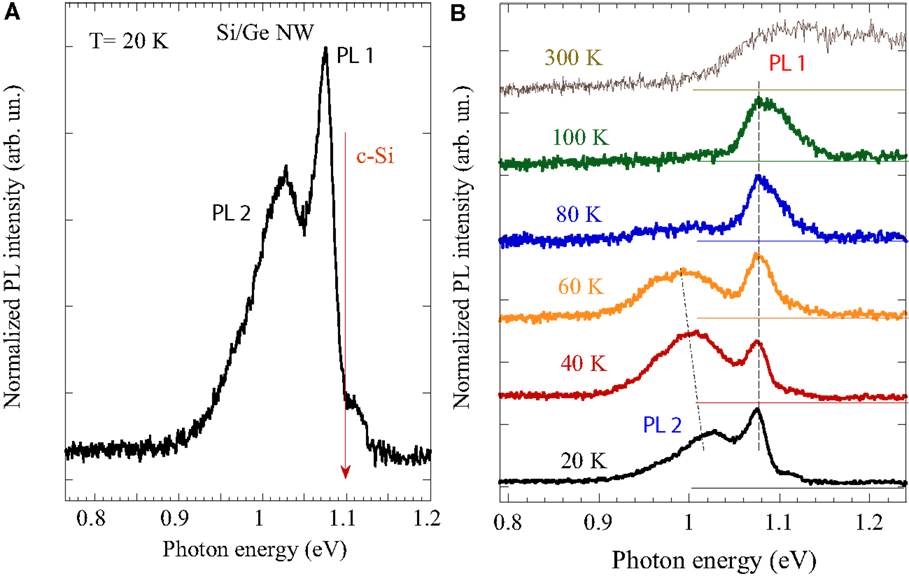
Figure 8. (A) Low-temperature photoluminescence (PL) spectrum of the Si/Ge NW HJs showing major peaks PL1 and PL2 and the location of the main (very sharp) PL peak in c-Si. (B) The PL spectra of the Si/Ge NW HJs at various (marked) temperatures. The PL spectra peak shift with temperature increase is indicated by dashed lines (Wang et al., 2015).
High-resolution TEM studies, analyses of lattice fringes, and EDX measurements (Figures 3–6) indicate that close to the center of the NW in the vicinity of the Si/Ge HJ the lattice-mismatch-induced strain is partially relaxed via spontaneous intermixing and the formation of a ~8-nm-thick SiGe transition layer. Additional structural relaxation occurs by gradual (within ~100 nm from the Si/Ge heterointerface) lateral expansion (i.e., increase in diameter) of the Ge segment of the NW (Figure 3). Close to the NW surface, we find a distortion in the lattice fringe patterns, which is easily detected by FFT analysis (Figure 5 box). These structural imperfections are located within a 2–3-nm-thick interface layer between the NW core and an oxide layer at the NW surface and they are slightly extended (up to 5–6 nm) toward the NW core in the vicinity of the Si/Ge NW HJs (Figure 5). We conclude that the Si/Ge NW HJs with a diameter approaching 70–100 nm can have a nearly perfect crystalline core and overall smaller density of structural defects (due to a lesser surface-to-volume ratio) compared to thinner NW HJs. The observation of an easily detectable PL signal (Figure 8) supports this conclusion and indicates that non-radiative recombination centers associated with the NW surface states do not fully control carrier recombination in Si/Ge NW HJs with diameters greater than 50 nm (which is the average diameter of NWs in our samples). Also, the PL1 peak is red-shifted by ~20 meV and considerably broadened compared to the c-Si PL spectrum, suggesting that the Si segment of the NW close to the Si/Ge HJ is non-uniformly strained. The PL associated with this segment of the Si/Ge NW HJ exhibits a peak shift toward higher photon energy as the temperature increases from 20 K to above room temperature, indicating that there is compressive stress due to the mismatch in Si and Ge CTEs and, possibly, NW bending. The PL peak at 1.03 eV (PL2) is even more broadened, and it disappears at T > 80K. We attributed PL2 to radiative carrier recombination within the SiGe alloy layer at the Si/Ge heterointerface (Chang et al., 2009). The PL2 peak position, significant PL2 intensity temperature dependence, and the PL signal disappearance at T > 80 K are consistent with exciton localization on compositional fluctuations in SiGe alloys (Kamenev et al., 2004). Thus, the structure of the interface region strongly affects carrier recombination in Si/Ge NW HJs.
Considering the Raman measurements, we anticipate that under the applied laser excitation intensity of 102–103 W/cm2, the sample temperature increases significantly. The Si–Si Raman peak position in Si/Ge NW HJs is in full agreement with the bulk c-Si Raman temperature dependence, but under 700 W/cm2 incident power density, the sample temperature is estimated to be ~680 K. This significant laser heating of our samples is due to a reduced thermal conductivity of the Si/Ge NW HJs and results in the behavior observed with increasing excitation power density described above. The temperature increase produces a strong shift of the Raman peak associated with the Si–Si(Ge) vibration mode toward higher wavenumbers, indicating strong (2–3 GPa) compressive strain, as also found from the PL data. This conclusion is supported by the Raman polarization dependence in Si/Ge axial NW HJs (Wang et al., 2015).
Quantum Dots
“By the 1990s, a different type of SiGe NS, namely the 3D self-assembled system produced by the well-known Stranski–Krastanov, or cluster-layer, growth mode in lattice-mismatched materials, had been demonstrated (Eaglesham and Cerullo, 1990; Mo et al., 1990; Jesson et al., 1993; Kamins et al., 1997; Baribeau et al., 2006). It has been shown that dislocation-free SiGe growth can be achieved using a higher temperature (≥600°C), and that the non-planar geometry is mainly responsible for the significant increase of the SiGe critical layer thickness. It has also been found that, compared to two-dimensional (2D) Si/SiGe NSs, the PL and EL quantum efficiency in 3D Si/SiGe NSs is higher (up to 1%), especially for T > 50 K (Cerdeira et al., 1972; Apetz et al., 1995; Schittenhelm et al., 1995; Schmidt et al., 1999b). Despite many successful demonstrations of PL and EL in the spectral range of 1.3–1.6 μm, which is important for optical fiber communications, the proposed further development of 3D Si/SiGe-based light emitters was discouraged by several studies, indicating a type II energy band alignment at Si/SiGe heterointerfaces (Van de Walle and Martin, 1986; Thewalt et al., 1997; Schittenhelm et al., 1998; El Kurdi et al., 2006), where the spatial separation of electrons (located in Si) and holes (localized in SiGe) (see Figure 1) was thought to make carrier radiative recombination very inefficient. Later, it was also shown that 3D Si/SiGe NSs exhibit an extremely long (of the order of 10−2 s) luminescence lifetime (Kamenev et al., 2005), which is of the order of a million times longer than in III–V semiconductors and their NSs. Thus, according to this analysis, 3D Si/SiGe NSs cannot be used to achieve efficient and commercially valuable light-emitting devices. Recently, however, it has been shown that despite the fact that the Si/SiGe heterointerface most likely exhibits type II energy band alignment, it is still possible to obtain conditions favorable for an efficient carrier radiative recombination.” For further details of this early work, see the additional review material given in Lockwood and Tsybeskov (2013).
With 3D confinement, the role of the dot surface and its interface with its surroundings becomes even more critical in determining the physical properties of SiGe NSs. In this section, we provide a summary of the latest time-resolved and continuous-wave (CW) PL investigations of the recombination dynamics of 3D Si/Si1−xGex multilayer NSs grown by MBE (Modi et al., 2012a,b; Lockwood et al., 2013b; Mala et al., 2013). Significantly, the Si/Si1−xGex NSs comprised a single Si1−xGex nanometer-thick layer (NL) integrated into Si/Si0.6Ge0.4 cluster multilayers (CMs).
Photoluminescence from SiGe Nanostructures
The PL spectra typically observed in 3D Si/SiGe NSs is similar to that found for III–V QWs with type II energy band alignment, as the PL exhibits a blue shift on increasing the excitation intensity (Lockwood and Tsybeskov, 2010). This effect is found in samples grown by both MBE and CVD. Figure 9A shows PL spectra in a CVD grown sample measured for different excitation intensities. At the lowest excitation intensity shown, the PL feature that is shown resolved into two components (see Figure 9A) peaks at ~0.8 eV. On increasing the excitation intensity, an unbroken PL blue shift of 30–40 meV for each decade of excitation intensity increase is observed (see Figure 9B). Under much higher photoexcitation intensity (1–10 kW/cm2), the low energy part of the PL spectrum does not shift any further, while the high energy part continues shifting toward higher energy. A modified Arrhenius plot of the normalized integrated PL intensity as a function of temperature for the different excitation intensities can be fitted with two thermal quenching activation energies, E1 and E2 (Lockwood and Tsybeskov, 2010). Activation energy E1 is found to be ~15 meV and is independent of the excitation intensity for all samples. Activation energy E2, however, depends considerably on the excitation intensity: it increases drastically from ~120 to 340 meV when the excitation intensity increases from 0.1 to 10 W/cm2. This high value for E2 implies that such PL can easily be observed at room temperature.
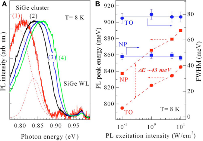
Figure 9. (A) Normalized low-temperature PL spectra in CVD grown Si/SiGe 3D nanostructures showing the PL spectral shift to higher photon energy under increasing CW excitation intensity [trace (1) 0.1, (2), 1, (3) 5, and (4) 10 W/cm2] at 2.41 eV (514.5 nm). Each spectrum can be fitted with two Gaussian spectral bands [the transverse-optic (TO) phonon replica and no-phonon (NP) lines, respectively], as shown, for example, by the dashed lines under trace (1). (B) The NP and TO line positions and widths [full-width at half maximum (FWHM)] as a function of excitation intensity (Lockwood and Tsybeskov, 2010).
Low-temperature PL dynamics have been measured for a CVD grown sample using a ~6-ns excitation pulse at 2.33 eV (532 nm) (Lockwood and Tsybeskov, 2010). The initial PL decay is fast (< 20 ns), close to the resolution of the detection system. However, a slower PL component demonstrates a strong dependence on the PL photon energy: at photon energies below 0.8 eV, the PL lifetime is found to be ~20 μs and then it drastically decreases to ~200 ns for PL observed at 0.89 eV.
Single Nanometer-Thick SiGe Nanocluster Sample
A TEM micrograph of a specially fabricated sample containing a very thin Si1−xGex cluster layer above a regular stack of such cluster layers that was grown using Si/SiGe MBE is shown in Figure 10A (Modi et al., 2012a). The sample is grown on a Si substrate and comprises two SiGe cluster layers with a cluster height of ~6–8 nm separated by a Si layer of ~8 nm thickness between the SiGe clusters (i.e., there are two SiGe/Si pairs); a 30-nm-thick Si spacer layer; another five SiGe/Si layer pairs to initiate 3D growth; a layer of SiGe clusters with a height of approximately 18 nm; a thinner separating Si layer; a final SiGe cluster layer; and a thin Si cap. The SiGe alloy cluster layers are composed of up to 40 atomic percent (at.%) Ge, and induce considerable global and local strain, which is readily visible in dark-field TEM imaging (see, for example, Figure 10B). Much of the strain is accommodated within a 60–70 nm depth of the Si substrate and within the 30-nm-thick Si spacer layer above it (see the bright regions in Figure 10B). The top two pairs of Si/SiGe layers, however, show a lower TEM contrast than the layers below them, primarily due to the much thinner (and strained) Si layer sandwiched between the two thicker SiGe cluster layers.
Figure 10. TEM micrographs showing (A) <011> zone axis bright-field TEM image and (B) {200} two-beam dark-field TEM image of the specially engineered Si/SiGe cluster multilayer nanostructure. The SiGe cluster layers are clearly seen as dark areas in Figure 10 (A) (Modi et al., 2012a).
A dark-field TEM image at greater magnification for the two Si/SiGe cluster layers closest to the Si substrate is presented in Figure 11 together with results from an EDX alloy-composition scan. As shown in Figure 10B, this region of the sample has a high strain and likely significant strain-induced Si/SiGe intermixing. The EDX analysis shows that the Ge atomic concentration at the Si/SiGe heterointerface increases from 0 to ~35 at.% within a distance d = 5 nm (Figure 11B). Figure 12 displays the corresponding information for the two topmost Si/SiGe clusters layers, where the Ge atomic concentration in the cluster reaches a maximum value of ~38 at.% within a much shorter distance d = 3 nm. The EDX scans, thus, reveal that the topmost Si/SiGe cluster layer has a much more abrupt Si/SiGe heterointerface compared to that found in the bottommost cluster layers.
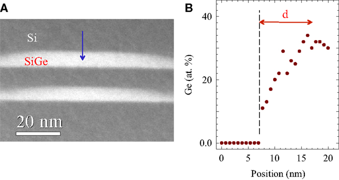
Figure 11. (A) A high angle annular dark-field scanning transmission electron microscope (HAADF-STEM) micrograph showing the first and second bottom SiGe cluster layers (counting from the Si substrate) and EDX scan position (arrow). (B) EDX measured Ge atomic concentration at the second bottom Si/SiGe cluster layer heterointerface. The interface abruptness d (which is the distance between pure Si and SiGe with the nominal Ge concentration) is indicated (Modi et al., 2012a).
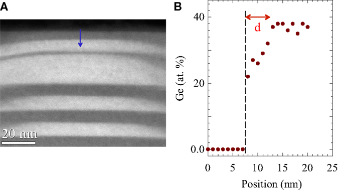
Figure 12. (A) A HAADF-STEM micrograph showing top SiGe cluster layers and EDX scan position (arrow). (B) EDX measured Ge atomic concentration at the topmost Si/SiGe cluster-layer heterointerface. The interface abruptness d is indicated (Modi et al., 2012a).
Photoluminescence measurements of this sample (see Figure 13A) reveal spectroscopic features that are consistent with the TEM and EDX data. Using photoexcitation at a wavelength of 405 nm, which has a penetration depth of ~0.1 μm, a PL peak is observed at 0.78 eV with a full-width at half maximum (FWHM) of ~130 meV. At an excitation wavelength of 325 nm with a penetration depth of only ~10 nm, the PL spectrum is shifted slightly toward lower photon energy and has a significantly reduced FWHM (~100 meV). This result demonstrates that the cluster composition and Si/SiGe interface abruptness, as illustrated in Figures 11 and 12, are influencing the PL behavior: the more abrupt the Si/SiGe interface, the smaller the FWHM of the PL peak, and, in the topmost SiGe layer, a higher Ge composition results in the PL peak being shifted toward lower photon energy (Modi et al., 2012a). In other similar samples, it has been shown that continuous optical excitation at shorter wavelengths produces substantial PL fatigue after a delay of about 10 min due to the accumulation of charge within the SiGe clusters (Modi et al., 2012b).
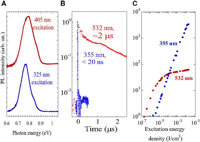
Figure 13. (A) Normalized low-temperature PL spectra (shifted vertically for clarity) collected for different excitation wavelengths. (B) The PL decays measured at 0.78 eV under ~6 ns duration pulsed excitation with the indicated excitation wavelengths. (C) The PL intensity as a function of excitation energy density at different excitation wavelengths. During these measurements, the sample temperature was 15 K (Modi et al., 2012a).
The PL lifetimes as a function of incident wavelength and PL intensity as a function of excitation energy density are shown in Figures 13B,C, respectively, both being measured under pulsed laser excitation with a pulse duration of ~6 ns. The PL excited at 532 nm and recorded at 0.78 eV, which originates predominantly from the lowermost Si/SiGe cluster layers, has a lifetime that is approximately 100 times longer than the same PL excited at 355 nm, which originates predominantly from the topmost Si/SiGe cluster layer. No changes in the PL lifetime are found under 355 nm excitation with energy densities varied from 10−5 to 5 × 10⁻² J/cm2 until the Auger limit has been reached, with the carrier concentration then approaching ~1019 cm−3 [see Figure 13C and Kamenev et al. (2005)]. There is a dramatic difference in the PL intensity as a function of excitation energy density for excitation at the two different wavelengths: the PL intensity under 532 nm excitation quickly saturates, in agreement with the findings of Kamenev et al. (2005) and Cerdeira et al. (1972), while, most impressively, the PL intensity under 355 nm excitation is linear versus excitation intensity for many orders of magnitude (see Figure 13C).
These results clearly demonstrate that in Si/SiGe 3D NSs the PL peaked near 0.78 eV strongly depends on the Si/SiGe heterointerface abruptness. The EDX measurements show that in conventional MBE-grown 3D Si/SiGe NSs the transition from pure Si to Si1−xGex with x = 0.3–0.4 in the cluster can require an intermixed SiGe interface whose width is more than 5 nm. These diffused type II Si/SiGe heterointerfaces are responsible for a significant electron–hole spatial separation (d > 5 nm) and the observed slow PL, which cannot compete with Auger recombination even at low optical excitation intensities. However, by means of growth engineering, more abrupt Si/SiGe heterointerfaces with, for example, d = 3 nm, can be obtained. These sharper heterointerfaces yield a PL lifetime of <20 ns, which remarkably is only a little slower than that found in direct band-gap III–V semiconductors. This extremely fast PL has a quite high quantum efficiency, which, in contrast to the previously reported results, remains constant over several orders of magnitude of optical excitation intensity.
Single Nanometer-Thick SiGe Quantum Well Sample
The specially prepared MBE-grown single QW sample is depicted in Figure 14A. The sample structure comprises a Si substrate (not visible in the TEM micrograph); a Si1−xGex buffer layer with x = 10 at.% (partly visible at the bottom of the micrograph); eight repeats of combined Si1−xGex cluster (reaching 10 nm thickness in the center) and Si layer pairs; a single 4–5 nm thick Si1−xGex NL followed by a thin Si layer; and a final Si1−xGex cluster layer capped with Si (Mala et al., 2013). The EDX scan of the sample shown in Figure 14B reveals that the Si1−xGex NL composition is relatively uniform (x = 8 at.%) while in the Si1−xGex clusters x monotonically increases from ~5 at.% at the Si/SiGe-cluster interface to up to 40 at.% at the cluster center.
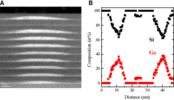
Figure 14. (A) A cross-sectional transmission electron micrograph (TEM) image showing the Si/SiGe NL/CM nanostructure with the very thin SiGe NL fourth from the top (Si) layer, and (B) energy-dispersive X-ray (EDX) measured composition of the sample’s six topmost layers. The arrow shows the direction of the EDX scan. The scale bar in the TEM image is 20 nm in length (Mala et al., 2014).
Two quite different PL spectra obtained using different excitation wavelengths but with approximately the same excitation intensities are compared in Figure 15A. The PL obtained under CW 325 nm excitation is peaked near 0.9 eV; whereas under 365 nm excitation, it is now peaked around 0.8 eV. PL spectra obtained with pulsed photoexcitation at 355 nm from a Nd:YAG laser are shown in Figure 15B. The time-integrated measurements were performed using a lock-in amplifier synchronized with the laser pulse; the accumulation time was in the range of 10−3–10−2 s. The PL peak intensity was measured at different wavelengths using a digital oscilloscope with an adjustable time window and employing a much shorter (~0.1 μs) accumulation time. As for the case of CW excitation at two different wavelengths, the two different techniques, although using the same excitation wavelength in this case, produced quite different PL results: the time-integrated spectrum exhibits a peak near 0.8 eV, while the maximum of the peak-intensity spectrum is at ~ 0.92 eV. Such differences in the PL spectra can be explained by a substantial difference in the lifetimes of the respective PL constituents. Earlier work has shown that the PL lifetime is indeed expected to be much shorter for the 0.92 eV peak compared with the 0.8 eV peak (Kamenev et al., 2005).
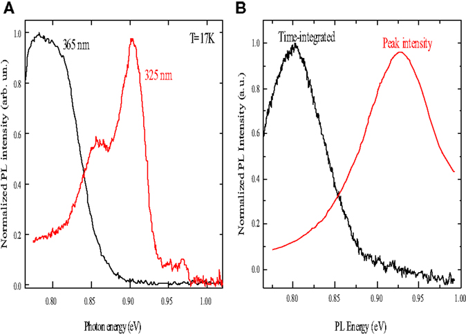
Figure 15. Low-temperature (17 K) PL spectra recorded under (A) CW excitation with the indicated excitation wavelengths and (B) pulsed 355-nm excitation using the time-integrated and peak-intensity methods (Mala et al., 2014).
The intensity of the 0.92 eV PL peak is linearly dependent on the excitation energy density with no saturation evident until an energy density of at least ~50 mJ/cm2, while the 0.8 eV PL peak intensity varies with excitation energy density as the square root (Mala et al., 2014). Also, the rise time of this latter PL peak decreases with both increasing excitation energy density and temperature.
The PL dynamics associated with the SiGe NL and the SiGe clusters using pulsed laser excitation at a wavelength of 355 nm and 6-ns long in duration are illustrated in Figure 16A. The 0.92 eV PL peak rises even faster than the system time resolution, while the 0.8 eV PL peak has a rise time of 2–3 μs. The former PL peak decays considerably faster compared to the latter PL peak. Non-exponential decays are exhibited by both kinds of PL bands. This suggests that in both cases the carrier recombination processes are characterized by a time-dependent recombination rate, Ri, and Figure 16B presents these rates that have been extracted from the PL decay data as a function of time. The recombination rate thus obtained is in the range of 106–107 s−1 for the 0.92 eV PL peak and is ~105–104 s−1 for the 0.8 eV peak PL.
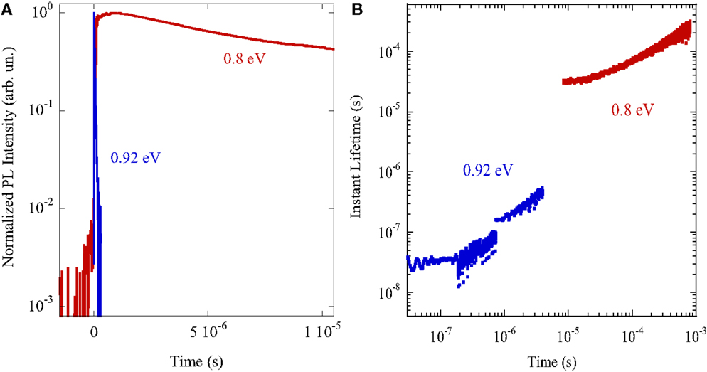
Figure 16. (A) Low-temperature (17 K) time-resolved PL decays under pulsed excitation energy density of 50 mJ/cm2 recorded at photon energies associated with SiGe NL PL (~ 0.92 eV) and SiGe cluster PL (~ 0.8 eV). (B) Carrier recombination rate as a function of time calculated using the PL decay data. The fast and slow PL decays are from the NL and clusters, respectively (Mala et al., 2014).
Interpretation Based on Interfacial Recombination
At low temperatures, carrier diffusion is known to be negligible in Si/SiGe NSs (Modi et al., 2012a). Hence, to account for the difference between the PL spectra obtained using shorter (325 nm) and longer (365 nm) wavelength excitation (see Figure 15A), one must allow for the difference in photoexcitation penetration depth, which is ~10−6 cm at 325 nm and ~10−5 cm at 365 nm (Paul, 2004; Modi et al., 2012a). Thus, the PL at ~ 0.9 eV is mostly associated with the 4–5-nm-thick Si1−xGex NL with x = 8 at.%, while the PL at ~ 0.8 eV is related to SiGe CMs with x reaching a maximum of 40 at.%. The PL in Si1−xGex CMs is shifted toward lower photon energies compared to that in bulk Si1−xGex alloys having a similar composition (Weber and Alonso, 1989), which is most likely due to the presence of strain and strain-induced Si/Si1−xGex interfacial mixing (Cerdeira et al., 1972; Schmidt and Eberl, 2000).
With pulsed laser excitation at 355 nm, the PL arising from both the SiGe NL and the SiGe CMs can be observed. The time-integrated PL signal shown in Figure 15B shows predominantly the PL peak at ~0.8 eV with a weak shoulder at ~0.9 eV, while the PL peak maximum intensity is now at ~0.92 eV (see Figure 15B). This indicates that the PL at 0.92 eV decays much faster than the 0.8 eV PL (Kamenev et al., 2005). It is noteworthy from the crystal quality point of view that in both the CW and time-resolved experiments no PL associated with crystallographic dislocations (Fukatsu et al., 1996) was found.
At a higher excitation energy density, the 0.8 eV peaked PL demonstrates a sub-linear dependence of the PL intensity on excitation energy density. However, the PL intensity of the 0.92 eV peak exhibits a linear dependence on the excitation energy density, indicating that the experimentally determined recombination rate of 106–107 s−1 is mostly due to radiative recombination. Given that Auger recombination is competing with radiative recombination, it is expected that the long-lived PL would saturate sooner than the short-lived PL. The experimental data in Figure 16A confirm that the decay of the PL peaked at 0.8 eV is indeed significantly slower when compared to that of the 0.92 eV PL peak. Figure 16A also shows that the 0.8 eV PL rise time of ~2–3 μs is much longer than the exciting laser pulse duration of ~6 ns. This exceptionally long PL rise time could be associated with a special kind of Auger-assisted carrier spatial redistribution in the Si/SiGe NSs that is termed the Auger fountain (Ohnesorge et al., 1996; Lee et al., 2009).
Non-exponential PL decays have been observed before in Si/SiGe NSs and analyzed by employing a stretched exponential function {exp[(–t/τ)β]}, a power function {1/(1 + αt)m}, or multiple exponential decays (Zrenner et al., 1995; Fukatsu et al., 1996; Kamenev et al., 2005). The stretched exponential PL decay phenomenon has been observed in a wide variety of systems apart from Si/SiGe NSs and it provides a good empirical fit to the data, although it most likely has no fundamental significance (Kuskovsky et al., 1998). Indeed, the underlying physical mechanism involved in non-exponential PL decay has yet to be identified. In a different approach to this issue, we extract the recombination rate directly from the PL decays without requiring any assumption or a specific physical model. Figure 16B indicates that initially both of the PL bands have an almost time-independent recombination rate, exhibiting single-exponential decays of ~9 × 10⁴ s−1 for the 0.8 eV PL band and ~3 × 10⁷ s−1 for the 0.92 eV PL band. The recombination rate decreases with increasing time, and varies as Ri(t)~t−α with α = 0.67 for the 0.8 eV PL band and α = 0.82 for the PL band peaked at 0.92 eV.
In accordance with the donor–acceptor pair recombination model (Thomas et al., 1965), the electron–hole time-dependent recombination rate can be explained by assuming that it depends on the average distance separating electrons and holes, ae–h. Due to the previously discussed type II energy band alignment at the Si/SiGe heterointerfaces, it is assumed that the holes are localized within the SiGe and the electrons are located in the Si. The recombination-rate dependence on this distance can be expressed as
where R0 is the maximum recombination rate (~108 s−1, see Figure 11B) and a0 is the minimal radius of the localized exciton at the Si/SiGe heterointerface (~1.5 nm). For the Si1−xGex NL with x ~ 8 at.%, ae–h ≤ 5 nm (a value that is comparable to the SiGe NL thickness) while in the Si1−xGex CMs where 0 ≤ x ≤ 40 at.%, ae–h is in the range of 9 nm < ae–h < 14 nm (see Figure 17). These results are consistent with the TEM and EDX data (see Figure 14). Thus, we again see that carrier migration and recombination are both strongly influenced by the NS interfacial characteristics.
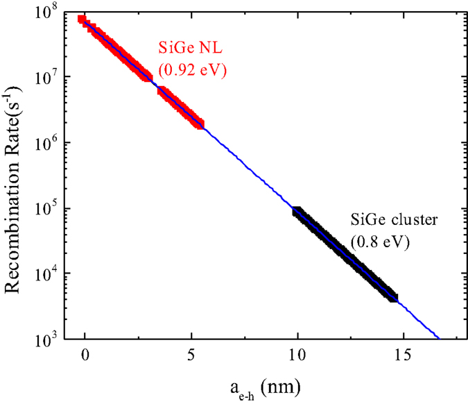
Figure 17. Carrier recombination rates (dots) extracted from the experimental data as a function of the distance between electrons and holes for photon detection energies associated with SiGe NL PL (~ 0.92 eV) and SiGe cluster PL (~ 0.8 eV). The solid line is the theoretically calculated electron–hole recombination rate (Mala et al., 2014).
Conclusion
The earlier studies and most recent investigations reported here of Si–Ge interfacial effects in SiGe NSs all demonstrate that for efficient carrier recombination and, hence, best device performance it is critical to ensure that the as-grown and possibly later-processed heterointerfaces are as sharp as possible. The sharpness is influenced by many factors, such as growth conditions, strain, and thermal processing, which in practice can make it difficult to attain the ideal structures required. This is certainly the case for NS confinement in one dimension.
However, we have demonstrated that axial Si/Ge NW HJs with good core crystallinity and fairly abrupt heterointerfaces can be fabricated using Au-catalyzed VLS growth. Spontaneous intermixing at the Si/Ge heterointerface and lateral expansion of the Ge segment of the nanowire partially relieves the lattice mismatch-induced strain. With a Si/Ge NW diameter in the range of 50–120 nm, surface-related structural defects and imperfections do not fully control carrier recombination in the Si/Ge NW HJs, and the PL signal associated with band-to-band electron–hole recombination at the Si/Ge NW HJ has readily been measured and attributed to a specific interfacial SiGe alloy composition revealed by EDX.
For 3D confinement, the experiments outlined here have shown that two quite different Si1−xGex NLs when amalgamated with a special Si0.6Ge0.4 CM structure exhibit strong PL that can have a characteristic decay time as much as 1000 times shorter than that found for PL in regular Si/SiGe CMs. The non-exponential PL decay observed in Si/SiGe NSs has been ascribed to differences in the distances separating electrons and holes across the Si/SiGe heterointerface. The results demonstrate that sharp Si/SiGe heterointerfaces can significantly reduce the carrier radiative recombination lifetime and thereby increase the PL quantum efficiency. These SiGe NL/CM combined NSs are now possible contenders for applications requiring light-emitting devices in CMOS compatible optoelectronics.
Author Contributions
DL planned and prepared most of this paper as well as participated in the experiments and their interpretation. XHW performed the electron microscopy work. J-MB prepared most of the samples used in this study. SM carried out some of the photoluminescence studies of some samples. XLW carried out some of the photoluminescence and Raman studies of some samples. LT planned and supervised the experimental work in NJIT and provided interpretation of the results.
Conflict of Interest Statement
The authors declare that the research was conducted in the absence of any commercial or financial relationships that could be construed as a potential conflict of interest.
Acknowledgments
This work is supported in part by NSF grant ECCS-1027770, Hewlett-Packard Laboratories and The Foundation at NJIT. We would like to acknowledge the invaluable contributions over a number of years from our many collaborators on this work and whose names are given in the references to our work in this paper. We thank especially B. Kamenev, E.-K. Lee, H. Y. Chang, and N. Modi of New Jersey Institute of Technology, and T. Kamins of Hewlett Packard Laboratories.
References
Abstreiter, G. (1998). “Chapter 2: band gaps and light emission in Si/SiGe atomic layer structures,” in Light Emission in Silicon, ed. D. J. Lockwood (San Diego: Academic Press), 37–76.
Ahn, D., Hong, C., Liu, J., Giziewicz, W., Beals, M., Kimerling, L. C., et al. (2007). High performance, waveguide integrated Ge photodetectors. Opt. Express 15, 3916. doi: 10.1364/OE.15.003916
Alonso, M. I., and Winer, K. (1989). Raman spectra of c-Si1− xGex alloys. Phys. Rev. B Condens. Matter. 39, 10056. doi:10.1103/PhysRevB.39.10056
Apetz, R., Vescan, L., Hartmann, A., Dieker, C., and Lüth, H. (1995). Photoluminescence and electroluminescence of SiGe dots fabricated by island growth. Appl. Phys. Lett. 66, 445–447. doi:10.1063/1.114051
Assefa, S., Xia, F., Bedell, S. W., Zhang, Y., Topuria, T., Rice, P. M., et al. (2010). CMOS-integrated high-speed MSM germanium waveguide photodetector. Opt. Express 18, 4986. doi:10.1364/OE.18.004986
Barbagiovanni, E. G., Cosentino, S., Lockwood, D. J., Costa Filho, R. N., Terrasi, A., and Mirabella, S. (2015). Influence of interface potential on the effective mass in Ge nanostructures. J. Appl. Phys. 117, 154304. doi:10.1063/1.4918549
Barbagiovanni, E. G., Lockwood, D. J., Simpson, P. J., and Goncharova, L. V. (2012). Quantum confinement in Si and Ge nanostructures. J. Appl. Phys. 111, 034307. doi:10.1063/1.3680884
Barbagiovanni, E. G., Lockwood, D. J., Simpson, P. J., and Goncharova, L. V. (2014). Quantum confinement in Si and Ge nanostructures: theory and experiment. Appl. Phys. Rev. 1, 011302. doi:10.1063/1.4835095
Baribeau, J.-M., Delâge, A., Janz, S., Lafontaine, H., Lockwood, D. J., McCaffrey, J. P., et al. (1999). “Wavy SiGe/Si superlattices: structural and optical properties and application to near infrared light detection,” in Advanced Luminescent Materials, Quantum Confinement, eds M. Cahay, S. Bandyopadhyay, N. Koshida, J. P. Leburton, D. J. Lockwood, M. Meyyappan, and T. Sakamoto (Pennington: Electrochemical Society), 45.
Baribeau, J.-M., Lockwood, D. J., and Syme, R. W. G. (1996). Interfaces in Si/Ge atomic layer superlattices on (001)Si: effect of growth temperature and wafer misorientation. J. Appl. Phys. 80, 1450. doi:10.1063/1.363013
Baribeau, J.-M., Pascual, R., and Saimoto, S. (1990). Interdiffusion and strain relaxation in (SimGen)p superlattices. Appl. Phys. Lett. 57, 1502–1504. doi:10.1063/1.103377
Baribeau, J.-M., Wu, X., Rowell, N. L., and Lockwood, D. J. (2006). Ge dots and nanostructures grown epitaxially on Si. J. Phys. Condens. Matter 18, R139. doi:10.1088/0953-8984/18/8/R01
Brey, L., and Tejedor, C. (1987). New optical transitions in Si-Ge strained superlattices. Phys. Rev. Lett. 59, 1022. doi:10.1103/PhysRevLett.59.1022
Camacho-Aguilera, R. E., Cai, Y., Patel, N., Bessette, J. T., Romagnoli, M., Kimerling, L. C., et al. (2012). An electrically pumped germanium laser. Opt. Express 20, 11316. doi:10.1364/OE.20.011316
Cerdeira, F., Dreybrodt, W., and Cardona, M. (1972). Resonant Raman scattering in germanium. Solid State Commun. 10, 591. doi:10.1016/0038-1098(72)90598-4
Chang, H. Y., Tsybeskov, L., Sharma, S., Kamins, T. I., Wu, X., and Lockwood, D. J. (2009). Photoluminescence and Raman scattering in axial Si/Ge nanowire heterojunctions. Appl. Phys. Lett. 95, 133120. doi:10.1063/1.3240595
Cosentino, S., Sungur Ozen, E., Raciti, R., Mio, A. M., Nicotra, G., Simone, F., et al. (2014). Light harvesting with Ge quantum dots embedded in SiO2 or Si3N4. J. Appl. Phys. 115, 043103. doi:10.1063/1.4863124
Eaglesham, D. J., and Cerullo, M. (1990). Dislocation-free Stranski–Krastanow growth of Ge on Si(100). Phys. Rev. Lett. 64, 1943–1946. doi:10.1103/PhysRevLett.64.1943
El Kurdi, M., Sauvage, S., Fishman, G., and Boucaud, P. (2006). Band-edge alignment of SiGe/Si quantum wells and SiGe/Si self-assembled islands. Phys. Rev. B Condens. Matter. 73, 195327–195336. doi:10.1103/PhysRevB.73.195327
Engvall, J., Olajos, J., Grimmeiss, H. G., Kibbel, H., and Presting, H. (1995). Luminescence from monolayer-thick Ge quantum wells embedded in Si. Phys. Rev. B Condens. Matter. 51, 2001. doi:10.1103/PhysRevB.51.2001
Engvall, J., Olajos, J., Grimmeiss, H. G., Presting, H., Kibbel, H., and Kasper, E. (1993). Electroluminescence at room temperature of a SinGem strained-layer superlattice. Appl. Phys. Lett. 63, 491. doi:10.1063/1.110780
Ertekin, E., Greaney, P. A., Chrzan, D. C., and Sands, T. D. (2005). Equilibrium limits of coherency in strained nanowire heterostructures. J. Appl. Phys. 97, 114325. doi:10.1063/1.1903106
Förster, M., Mantz, U., Ramminger, S., Thonke, K., Sauer, R., Kibbel, H., et al. (1996). Electroluminescence, photoluminescence, and photocurrent studies of Si/SiGe p-i-n heterostructures. J. Appl. Phys. 80, 3017. doi:10.1063/1.363129
Froyen, S., Wood, D. M., and Zunger, A. (1987). New optical transitions in strained Si-Ge superlattices. Phys. Rev. B Condens. Matter. 36, 4547. doi:10.1103/PhysRevB.36.4547
Fukatsu, S., Mera, Y., Inoue, M., Maeda, K., Akiyama, H., and Sakaki, H. (1996). Time-resolved D-band luminescence in strain-relieved SiGe/Si. Appl. Phys. Lett. 68, 1889–1891. doi:10.1063/1.116284
Fukatsu, S., Usami, N., Chinzei, T., Shiraki, Y., Nishida, A., and Nakagawa, K. (1992). Electroluminescence from strained SiGe/Si quantum well structures grown by solid source Si molecular beam epitaxy. Jpn. J. Appl. Phys. 31, L1015. doi:10.1143/JJAP.31.L1018
Gnutzman, U., and Clausecker, K. (1974). Theory of direct optical transitions in an optical indirect semiconductor with a superlattice structure. Appl. Phys. 3, 9. doi:10.1007/BF00892328
Grydlik, M., Hackl, F., Groiss, H., Glaser, M., Halilovic, A., Fromherz, T., et al. (2016). Lasing from Glassy Ge Quantum Dots in Crystalline Si. ACS Photonics 3, 298–303. doi:10.1021/acsphotonics.5b00671
Guerra, R., Marsili, M., Pulci, O., and Ossicini, S. (2011). Local-field effects in silicon nanoclusters. Phys. Rev. B 84, 075342. doi:10.1103/PhysRevB.84.075342
Guerra, R., and Ossicini, S. (2010). High luminescence in small Si/SiO2 nanocrystals: a theoretical study. Phys. Rev. B 81, 245307. doi:10.1103/PhysRevB.81.245307
Hannon, J. B., Kodambaka, S., Ross, F. M., and Tromp, R. M. (2006). The influence of the surface migration of gold on the growth of silicon nanowires. Nature 440, 69. doi:10.1038/nature04574
Houghton, D. C., Aers, G. C., Eric Yang, S. R., Wang, E., and Rowell, N. L. (1995). Type I band alignment in Si1-xGex/Si(001) quantum wells: photoluminescence under applied [110] and [100] uniaxial stress. Phys. Rev. Lett. 75, 866–869. doi:10.1103/PhysRevLett.75.866
Hybertsen, M. S., and Schlüter, M. (1987). Theory of optical transitions in Si/Ge (001) strained-layer superlattices. Phys. Rev. B Condens. Matter. 36, 9683. doi:10.1103/PhysRevB.36.9683
Iyer, S. S., Patton, G. L., Stork, J., Meyerson, B. S., and Harame, D. L. (1989). Heterojunction bipolar transistors using Si-Ge alloys. IEEE Trans. Electron Devices 36, 2043. doi:10.1109/16.40887
Jackson, S. A., and People, R. (1986). Optical absorption probability for the zone-folding induced quasi-direct gap in Ge(x)Si(1− x)/Si strained layer superlattices. MRS Proc. 56, 365. doi:10.1557/PROC-56-365
Jesson, D. E., Pennycook, S. J., Tischler, J. Z., Budai, J. D., Baribeau, J.-M., and Houghton, D. C. (1993). Interplay between evolving surface morphology, atomic-scale growth modes, and ordering during SixGe1-x epitaxy. Phys. Rev. Lett. 70, 2293–2296. doi:10.1103/PhysRevLett.70.2293
Kamenev, B. V., Lee, E.-K., Chang, H.-Y., Han, H., Grebel, H., Tsybeskov, L., et al. (2006). Excitation-dependent photoluminescence in Ge/Si Stranski–Krastanov nanostructures. Appl. Phys. Lett. 89, 153106–153108. doi:10.1063/1.2361198
Kamenev, B. V., Tsybeskov, L., Baribeau, J.-M., and Lockwood, D. J. (2004). Photoluminescence and Raman scattering in three-dimensional Si/Si1-xGex nanostructures. Appl. Phys. Lett. 84, 1293. doi:10.1063/1.1650873
Kamenev, B. V., Tsybeskov, L., Baribeau, J.-M., and Lockwood, D. J. (2005). Coexistence of fast and slow luminescence in three-dimensional Si/Si1-xGex nanostructures. Phys. Rev. B 72, 193306–193309. doi:10.1103/PhysRevB.72.193306
Kamins, T. I., Carr, E. C., Williams, R. S., and Rosner, S. J. (1997). Deposition of three-dimensional Ge islands on Si(001) by chemical vapor deposition at atmospheric and reduced pressures. J. Appl. Phys. 81, 211–219. doi:10.1063/1.364084
Kamins, T. I., Li, X., Williams, R. S., and Liu, X. (2004). Growth and structure of chemically vapor deposited Ge nanowires on Si substrates. Nano Lett. 4, 503. doi:10.1021/nl035166n
Kasper, E., and Schäffler, F. (1991). “Strained-layer superlattices,” in Materials Science and Technology, ed. T. P. Pearsall (Boston: Academic Press), 223.
Kästner, G., and Gösele, U. (2004). Stress and dislocations at cross-sectional heterojunctions in a cylindrical nanowire. Philos. Mag. A 84, 3803. doi:10.1080/1478643042000281389
Kato, Y., Fukatsu, S., and Shiraki, Y. (1995). Postgrowth of a Si contact layer on an air-exposed Si1− xGex/Si single quantum well grown by gas-source molecular beam epitaxy, for use in an electroluminescent device. J. Vac. Sci. Technol. B 13, 111. doi:10.1116/1.588002
Kuskovsky, I., Neumark, G. F., Bondarev, V. N., and Pikhitsa, P. V. (1998). Decay dynamics in disordered systems: application to heavily doped semiconductors. Phys. Rev. Lett. 80, 2413–2416. doi:10.1103/PhysRevLett.80.2413
Lauhon, L. J., Gudiksen, M. S., Wang, D., and Lieber, C. M. (2002). Epitaxial core–shell and core–multishell nanowire heterostructures. Nature 420, 57. doi:10.1038/nature01141
Lee, E.-K., Lockwood, D. J., Baribeau, J.-M., Bratkovsky, A. M., Kamins, T. I., and Tsybeskov, L. (2009). Photoluminescence dynamics and Auger fountain in three-dimensional Si/SiGe multilayer nanostructures. Phys. Rev. B Condens. Matter. 79, 233307–233307. doi:10.1103/PhysRevB.79.233307
Lenchyshyn, L. C., Thewalt, M. L. W., Houghton, D. C., Noël, J.-P., Rowell, N. L., Sturm, J. C., et al. (1993). Photoluminescence mechanisms in thin Si1− xGex quantum wells. Phys. Rev. B Condens. Matter. 47, 16655. doi:10.1103/PhysRevB.47.16655
Lenchyshyn, L. C., Thewalt, M. L. W., Sturm, J. C., Schwartz, P. V., Prince, E. J., Rowell, N. L., et al. (1992). High quantum efficiency photoluminescence from localized excitons in Si1− xGex. Appl. Phys. Lett. 60, 3174. doi:10.1063/1.106733
Liu, J., Sun, X., Camacho-Aguilera, R., Kimerling, L. C., and Michel, J. (2010). Ge-on-Si laser operating at room temperature. Opt. Lett. 35, 679. doi:10.1364/OL.35.000679
Liu, J., Sun, X., Kimerling, L. C., and Michel, J. (2009). Direct-gap optical gain of Ge on Si at room temperature. Opt. Lett. 34, 1738. doi:10.1364/OL.34.001738
Lockwood, D. J. (1998). “Light emission in silicon,” in Light Emission in Silicon: From Physics to Devices, ed. D. J. Lockwood (San Diego: Academic Press), 1–36.
Lockwood, D. J., Baribeau, J.-M., Jackman, T. E., Aebi, P., Tyliszczak, T., Hitchcock, A. P., et al. (1993). Influence of annealing on the interface structure and strain relief in Si/Ge heterostructures on (100) Si. Scanning Microsc. 7, 457.
Lockwood, D. J., Rowell, N. L., Barbagiovanni, E. G., Goncharova, L. V., Simpson, P. J., Berbezier, I., et al. (2013a). Photoluminescence efficiency of germanium dots self-assembled on oxides. ECS Trans. 53, 185. doi:10.1149/05301.0185ecst
Lockwood, D. J., Wu, X., Baribeau, J.-M., Modi, N., and Tsybeskov, L. (2013b). Fast luminescence in silicon-germanium nanostructures. ECS Trans. 50, 35–47. doi:10.1149/05041.0035ecst
Lockwood, D. J., and Tsybeskov, L. (2010). “Three-dimensional silicon-germanium nanostructures for CMOS compatible light emitters,” in Nanotechnology for Electronics, Photonics, and Renewable Energy, eds A. Korkin, P. S. Krstić, and J. C. Wells (New York: Springer), 41–84.
Lockwood, D. J., and Tsybeskov, L. (2013). “Light emission in Si/SiGe nanostructures,” in Handbook of Silicon Photonics, eds L. Vivien and L. Pavesi (Boca Raton, FL: CRC Press), 354–371.
Lu, Z. H., Baribeau, J.-M., and Lockwood, D. J. (1994). Surface segregation during Si/Gen/Si(100) interface formation. J. Appl. Phys. 76, 3911. doi:10.1063/1.357399
Lu, Z. H., Lockwood, D. J., and Baribeau, J.-M. (1995). Quantum confinement and light emission in SiO2/Si superlattices. Nature 378, 258–260. doi:10.1038/378258a0
Mala, S. A., Tsybeskov, L., Lockwood, D. J., Wu, X., and Baribeau, J.-M. (2013). Fast and intense photoluminescence in a SiGe nano-layer embedded in multilayers of Si/SiGe clusters. Appl. Phys. Lett. 103, 033103–033103–3. doi:10.1063/1.4813560
Mala, S. A., Tsybeskov, L., Lockwood, D. J., Wu, X., and Baribeau, J.-M. (2014). Carrier recombination in multilayers Si/Si1-xGex nanostructures. Physica B Condens. Matter. 453, 29. doi:10.1016/j.physb.2014.03.084
Mangolini, L. (2013). Synthesis, properties, and applications of silicon nanocrystals. J. Vac. Sci. Technol. B 31, 020801. doi:10.1116/1.4794789
Menczigar, U., Abstreiter, G., Olajos, J., Grimmeiss, H. G., Kibbel, H., Presting, H., et al. (1993). Enhanced bandgap luminescence in strain-symmetrized (Sim)/(Gen) superlattices. Phys. Rev. B Condens. Matter. 47, 4099. doi:10.1103/PhysRevB.47.4099
Menczigar, U., Brunner, J., Freiss, E., Gail, M., Abstreiter, G., Kibbel, H., et al. (1992). Photoluminescence studies of Si/Si1− xGex quantum wells and SimGen superlattices. Thin Solid Films 222, 227. doi:10.1016/0040-6090(92)90074-L
Mi, Q., Xiao, X., Sturm, J. C., Lenchyshyn, L. C., and Thewalt, M. L. W. (1992). Room-temperature 1.3 μm electroluminescence from strained Si1− xGex/Si quantum wells. Appl. Phys. Lett. 60, 3177. doi:10.1063/1.106734
Michel, J., Liu, J., and Kimerling, L. C. (2010). High-performance Ge-on-Si photodetectors. Nat. Photonics 4, 527. doi:10.1038/nphoton.2010.157
Mo, Y. W., Savage, D. E., Swartzentruber, B. S., and Lagally, M. G. (1990). Kinetic pathway in Stranski–Krastanov growth of Ge on Si (001). Phys. Rev. Lett. 65, 1020–1023. doi:10.1103/PhysRevLett.65.1020
Modi, N., Lockwood, D. J., Baribeau, J.-M., Wu, X., and Tsybeskov, L. (2012a). Excitation wavelength dependent photoluminescence in structurally non-uniform Si/SiGe-island heteroepitaxial multilayers. J. Appl. Phys. 111, 114313–114313–5. doi:10.1063/1.4729077
Modi, N., Tsybeskov, L., Baribeau, J.-M., Wu, X., and Lockwood, D. J. (2012b). Photoluminescence fatigue in three-dimensional silicon/silicon-germanium nanostructures. J. Appl. Phys. 111, 064318–064318–3. doi:10.1063/1.3698303
Nayak, D. K., Goto, K., Yutani, A., Murota, J., and Shiraki, Y. (1996). High-mobility strained-Si PMOSFET’s. IEEE Trans. Electron Devices 43, 1709. doi:10.1109/16.536817
Noël, J.-P., Rowell, N. L., Houghton, D. C., and Perovic, D. D. (1990). Intense photoluminescence between 1.3 and 1.8 μm from strained Si1− xGex alloys. Appl. Phys. Lett. 57, 1037. doi:10.1063/1.103558
Noël, J.-P., Rowell, N. L., Houghton, D. C., Wang, A., and Perovic, D. D. (1992). Luminescence origins in molecular beam epitaxial Si1− xGex. Appl. Phys. Lett. 61, 690. doi:10.1063/1.107823
Ohnesorge, B., Albrecht, M., Oshinowo, J., Forchel, A., and Arakawa, Y. (1996). Rapid carrier relaxation in self-assembled InxGa1-xAs/GaAs quantum dots. Phys. Rev. B Condens. Matter. 54, 11532–11538. doi:10.1103/PhysRevB.54.11532
Omura, Y., Gamiz, F., Nguyen, B.-Y., Ishii, H., Martino, J. A., Selberherr, S., et al. (2013). Advanced Semiconductor-on-Insulator Technology and Related Physics 16. Pennington, NJ: Electrochemical Society.
Orner, B. A., Olowolafe, J., Roe, K., Kolodzey, J., Laursen, T., Mayer, J. W., et al. (1996). Band gap of Ge rich Si1− x− yGexCy alloys. Appl. Phys. Lett. 69, 2557. doi:10.1063/1.117738
Paul, D. J. (2004). Si/SiGe heterostructures: from material and physics to devices and circuits. Semicond. Sci. Technol. 19, R75–R108. doi:10.1088/0268-1242/19/10/R02
Pavesi, L., Negro, L. D., Mazzoleni, C., Franzo, G., and Priolo, F. (2000). Optical gain in silicon nanocrystals. Nature 408, 440–444. doi:10.1038/35044012
Pearsall, T. P. (1994). Electronic and optical properties of Ge-Si superlattices. Prog. Quant. Electron. 18, 97–152. doi:10.1016/0079-6727(94)90006-X
Pearsall, T. P., Bevk, J., Feldman, L. C., Bonar, J. M., Mannaerts, J. P., and Ourmarzd, A. (1987). Structurally induced optical transitions in Ge-Si superlattices. Phys. Rev. Lett. 58, 729. doi:10.1103/PhysRevLett.58.1053
People, R., and Jackson, S. A. (1987). Indirect, quasidirect, and direct optical transitions in the pseudomorphic (44)-monolayer Si-Ge strained-layer superlattice on Si (001). Phys. Rev. B Condens. Matter. 36, 1310. doi:10.1103/PhysRevB.36.1310
People, R., and Jackson, S. A. (1990). “Structurally induced states from strain and confinement,” in Strained Layer Superlattices: Physics, ed. T. P. Pearsall (Boston: Academic Press), 119.
Presting, H., Menczigar, U., Abstreiter, G., Kibbel, H., and Kasper, E. (1992a). Electro and photoluminescence from ultrathin SimGen superlattices. MRS Proc. 256, 83. doi:10.1557/PROC-256-83
Presting, H., Kibbel, H., Jaros, M., Turton, R. M., Menczigar, U., Abstreiter, G., et al. (1992b). Ultrathin SimGen strained layer superlattices – a step towards Si optoelectronics. Semicond. Sci. Technol. 7, 1127. doi:10.1088/0268-1242/7/9/001
Presting, H., Zinke, T., Splett, A., Kibbel, H., and Jaros, M. (1996). Room-temperature electroluminescence from Si/Ge/Si1− xGex quantum-well diodes grown by molecular-beam epitaxy. Appl. Phys. Lett. 69, 2376. doi:10.1063/1.117642
Ray, S. K., Maikap, S., Banerjee, W., and Das, S. (2013). Nanocrystals for silicon-based light-emitting and memory devices. J. Phys. D Appl. Phys. 46, 153001. doi:10.1088/0022-3727/46/15/153001
Robbins, D. J., Calcott, P., and Leong, W. Y. (1991). Electroluminescence from a pseudomorphic Si0. 8Ge0. 2 alloy. Appl. Phys. Lett. 59, 1350. doi:10.1063/1.105305
Robbins, D. J., Canham, L. T., Barnett, S. J., Pitt, A. D., and Calcott, P. (1992). Near-band-gap photoluminescence from pseudomorphic Si1-xGex single layers on silicon. J. Appl. Phys. 71, 1407–1414. doi:10.1063/1.351262
Rowell, N. L., Noël, J.-P., Houghton, D. C., and Buchanan, M. (1990). Electroluminescence and photoluminescence from Si1− xGex alloys. Appl. Phys. Lett. 58, 957. doi:10.1063/1.104454
Rowell, N. L., Noël, J.-P., Houghton, D. C., Wang, A., Lenchyshyn, L. C., Thewalt, M. L. W., et al. (1993). Exciton luminescence in Si1− xGex/Si heterostructures grown by molecular beam epitaxy. J. Appl. Phys. 74, 2790. doi:10.1063/1.354628
Saraswat, K., Chui, C. O., Krishnamohan, T., Kim, D., Nayfeh, A., and Pethe, A. (2006). High performance germanium MOSFETs. Mater. Sci. Eng. B 135, 242. doi:10.1016/j.mseb.2006.08.014
Savage, D. E., Liu, F., Zielasek, V., and Lagaly, M. G. (1999). “Fundamental mechanisms of film growth,” in Germanium Silicon: Growth and Materials, Semiconductor and Semimetals, Vol. 56, eds R. Hull and J. C. Bean (New York: Academic Press), 49–96.
Schittenhelm, P., Engel, C., Findeis, F., Abstreiter, G., Darhuber, A. A., Bauer, G., et al. (1998). Self-assembled Ge dots: growth, characterization, ordering, and applications. J. Vac. Sci. Technol. B 16, 1575–1581. doi:10.1116/1.589942
Schittenhelm, P., Gail, M., Brunner, J., Nützel, J. F., and Abstreiter, G. (1995). Photoluminescence study of the crossover from two-dimensional to three-dimensional growth for Ge on Si(100). Appl. Phys. Lett. 67, 1292–1294. doi:10.1063/1.114401
Schmidt, O. G., and Eberl, K. (2000). Multiple layers of self-assembled Ge/Si islands: photoluminescence, strain fields, material interdiffusion, and island formation. Phys. Rev. B Condens. Matter. 61, 13721–13729. doi:10.1103/PhysRevB.61.13721
Schmidt, O. G., Kienzle, O., Hao, Y., Eberl, K., and Ernst, F. (1999a). Modified Stranski–Krastanov growth in stacked layers of self-assembled islands. Appl. Phys. Lett. 74, 1272. doi:10.1063/1.123522
Schmidt, O. G., Lange, C., and Eberl, K. (1999b). Photoluminescence study of the initial stages of island formation for Ge pyramids/domes and hut clusters on Si(001). Appl. Phys. Lett. 75, 1905–1907. doi:10.1063/1.124867
Shah, V. A., Dobbie, A., Myronov, M., and Leadley, D. R. (2010). Reverse graded SiGe/Ge/Si buffers for high-composition virtual substrates. J. Appl. Phys. 107, 064304. doi:10.1063/1.3311556
Shin, H. K., Lockwood, D. J., and Baribeau, J. -M. (2000). Strain in coherent-wave SiGe/Si superlattices. Solid State Commun. 114, 505. doi:10.1016/S0038-1098(00)00111-3
Shiraki, Y., and Sakai, A. (2005). Fabrication technology of SiGe hetero-structures and their properties. Surf. Sci. Rep. 59, 153–207. doi:10.1016/j.surfrep.2005.08.001
Soref, R. A., Atzman, Z., Shaapur, F., Robinson, M., and Westhoff, R. (1996). Infrared waveguiding in Si1− x− y GexCy upon silicon. Optics Lett. 21, 345. doi:10.1364/OL.21.000345
St Amour, A., Liu, C. W., Sturm, J. C., Lacroix, Y., and Thewalt, M. L. W. (1995). Defect-free band-edge photoluminescence and band gap measurement of pseudomorphic Si1− x− yGexCy alloy layers on Si (100). Appl. Phys. Lett. 67, 3915. doi:10.1063/1.115316
Stoica, T., Vescan, L., and Goryll, M. (1998). Electroluminescence of strained SiGe/Si selectively grown above the critical thickness for plastic relaxation. J. Appl. Phys. 83, 3367. doi:10.1063/1.367104
Sturm, J. C. (1998). Advanced column-IV epitaxial materials for silicon-based optoelectronics. MRS Bull. 23, 60.
Sturm, J. C., Manoharan, H., Lenchyshyn, L. C., Thewalt, M. L. W., Rowell, N. L., Noël, J.-P., et al. (1991). Well-resolved band-edge photoluminescence of excitons confined in strained Si1-xGex quantum wells. Phys. Rev. Lett. 66, 1362–1365. doi:10.1103/PhysRevLett.66.1362
Thewalt, M. L. W., Harrison, D. A., Reinhart, C. F., Wolk, J. A., and Lafontaine, H. (1997). Type II band alignment in Si1-xGex/Si(001) quantum wells: the ubiquitous type I luminescence results from band bending. Phys. Rev. Lett. 79, 269–272. doi:10.1103/PhysRevLett.79.269
Thomas, D. G., Hopfield, J. J., and Augustyniak, W. M. (1965). Kinetics of radiative recombination at randomly distributed donors and acceptors. Phys. Rev. 140, A202–A220. doi:10.1103/PhysRev.140.A202
Tsybeskov, L., and Lockwood, D. J. (2009). Silicon-germanium nanostructures for light emitters and on-chip optical interconnects. Proc. IEEE 97, 1284–1303. doi:10.1109/JPROC.2009.2020711
Tsybeskov, L., Moore, K. L., Hall, D. G., and Fauchet, P. M. (1996). Intrinsic band-edge photoluminescence from silicon clusters at room temperature. Phys. Rev. B Condens. Matter. 54, R8361. doi:10.1103/PhysRevB.54.R8361
Van de Walle, C. G., and Martin, R. M. (1986). Theoretical calculations of heterojunction discontinuities in Si/Ge system. Phys. Rev. B Condens. Matter. 34, 5621–5634. doi:10.1103/PhysRevB.34.5621
Vescan, L., and Stoica, T. (1998). Room-temperature SiGe light-emitting diodes. J. Luminescence 80, 485. doi:10.1016/S0022-2313(98)00160-4
Wagner, R. S. (1970). “Growth of crystals by the vapour–liquid–solid mechanism,” in Whisker Technology, ed. A. P. Levitt (New York: Wiley), 47.
Wang, X., Tsybeskov, L., Kamins, T. I., Wu, X., and Lockwood, D. J. (2015). Structural and optical properties of axial silicon-germanium nanowire heterojunctions. J. Appl. Phys. 118, 234301. doi:10.1063/1.4937345
Weber, J., and Alonso, M. I. (1989). Near-band-gap photoluminescence of Si-Ge alloys. Phys. Rev. B Condens. Matter. 40, 5683–5693. doi:10.1103/PhysRevB.40.5683
Xiang, J., Lu, W., Hu, Y., Wu, Y., Yan, H., and Lieber, C. M. (2006). Ge/Si nanowire heterostructures as high-performance field-effect transistors. Nature 441, 489. doi:10.1038/nature04796
Ye, H., and Yu, J. (2014). Germanium epitaxy on silicon. Sci. Technol. Adv. Mater. 15, 024601. doi:10.1088/1468-6996/15/2/024601
Yin, T., Cohen, R., Morse, M. M., Sarid, G., Chetrit, Y., Rubin, D., et al. (2007). 31 GHz Ge nip waveguide photodetectors on silicon-on-insulator substrate. Opt. Express 15, 13965. doi:10.1364/OE.15.013965
Zachai, R., Eberl, K., Abstreiter, G., Kasper, H., and Kibbel, H. (1990). Photoluminescence in short-period Si/Ge strained-layer superlattices. Phys. Rev. Lett. 64, 1055. doi:10.1103/PhysRevLett.64.1055
Zakharov, N. D., Werner, P., Gerth, G., Schubert, L., Sokolov, L., and Gösele, U. (2006). Growth phenomena of Si and Si/Ge nanowires on Si (111) by molecular beam epitaxy. J. Cryst. Growth 290, 6. doi:10.1016/j.jcrysgro.2005.12.096
Zheng, B., Michel, J., Ren, F. Y. G., Kimerling, L. C., Jacobson, D. C., and Poate, J. M. (1994). Room-temperature sharp line electroluminescence at λ=1.54 μm from an erbium-doped, silicon light-emitting diode. Appl. Phys. Lett. 64, 2842–2844. doi:10.1063/1.111977
Zrenner, A., Fröhlich, B., Brunner, J., and Abstreiter, G. (1995). Time-resolved photoluminescence of pseudomorphic SiGe quantum wells. Phys. Rev. B Condens. Matter. 52, 16608–16611. doi:10.1103/PhysRevB.52.16608
Keywords: silicon, germanium, nanostructures, heterointerface, photoluminescence, quantum, confinement, interfaces
Citation: Lockwood DJ, Wu X, Baribeau J-M, Mala SA, Wang X and Tsybeskov L (2016) Si/SiGe Heterointerfaces in One-, Two-, and Three-Dimensional Nanostructures: Their Impact on SiGe Light Emission. Front. Mater. 3:12. doi: 10.3389/fmats.2016.00012
Received: 05 October 2015; Accepted: 15 February 2016;
Published: 07 March 2016
Edited by:
Manuel João Mendes, Centro de Investigação em Materiais – I3N, PortugalReviewed by:
Larysa Yu. Khomenkova, National Academy of Sciences of Ukraine, UkraineTatiana S. Perova, Trinity College Dublin, Ireland
Copyright: © 2016 Lockwood, Wu, Baribeau, Mala, Wang and Tsybeskov. This is an open-access article distributed under the terms of the Creative Commons Attribution License (CC BY). The use, distribution or reproduction in other forums is permitted, provided the original author(s) or licensor are credited and that the original publication in this journal is cited, in accordance with accepted academic practice. No use, distribution or reproduction is permitted which does not comply with these terms.
*Correspondence: David J. Lockwood, david.lockwood@nrc-cnrc.gc.ca