Advances on Sensitive Electron-Injection Based Cameras for Low-Flux, Short-Wave Infrared Applications
 Vala Fathipour
 Alireza Bonakdar
  Hooman Mohseni
- Northwestern University, Evanston, IL, USA
Short-wave infrared (SWIR) photon detection has become an essential technology in the modern world. Sensitive SWIR detector arrays with high pixel density, low noise levels, and high signal-to-noise-ratios are highly desirable for a variety of applications including biophotonics, light detection and ranging, optical tomography, and astronomical imaging. As such many efforts in infrared detector research are directed toward improving the performance of the photon detectors operating in this wavelength range. We review the history, principle of operation, present status, and possible future developments of a sensitive SWIR detector technology, which has demonstrated to be one of the most promising paths to high pixel density focal plane arrays (FPAs) for low flux applications. The so-called electron-injection (EI) detector was demonstrated for the first time in 2007. It offers an overall system-level sensitivity enhancement compared to the p–i–n diode due to a stable internal avalanche-free gain. The amplification method is inherently low noise, and devices exhibit an excess noise of unity. The detector operates in linear-mode and requires only bias voltage of a few volts. This together with the feedback stabilized gain mechanism, makes formation of large-format high pixel density electron-injection FPAs less challenging compared to other detector technologies such as avalanche photodetectors. Detector is based on the mature InP material system and has a cutoff wavelength of 1700 nm. The layer structure consists of 500 nm InP injector/50 nm InAlAs etch stop/50 nm GaAsSb electron barrier (and hole trap)/1 μm InGaAs absorber. The epitaxial layers are grown on InP substrates. Electron-injection detector takes advantage of a unique three-dimensional geometry and combines the efficiency of a large absorbing volume with the sensitivity of a low-dimensional switch (injector) to sense and amplify signals. EI detectors have been designed, fabricated, and tested during two generations of development and optimization cycles. We review our imager results using the first-generation detectors. In the second-generation devices, the dark current is reduced by two orders of magnitude, and bandwidth is improved by four orders of magnitude. The dark current density of the second-generation EI detector is shown to outperform the state-of-the-art technology, the SWIR HgCdTe eAPD by more than one order of magnitude. We demonstrate a performance comparison with other SWIR detector technologies with internal amplification and show that the electron-injection detectors offer more than three orders of magnitude better noise-equivalent sensitivity compared with state-of-the-art phototransistors operating at similar temperature. Second-generation devices provide high-speed response ~6 ns rise time, low jitter ~12 ps, high amplification of more than 1000, unity excess noise factor, and operate at bias voltage of –3 V, at room temperature. The internal dark current density is ~1 μA/cm2 at room temperature decreasing to 1 nA/cm2 at 210 K. These improvements have opened up many applications for these detectors in the medical field, remote sensing, and exoplanet detection.
Introduction
Highly sensitive detector arrays in the short-wave infrared (SWIR) band spanning from 1 to 2.5 μm in the electromagnetic spectrum have wide applications. These include biophotonics (Matousek and Stone, 2013), astronomy (Schindler et al., 2014), optical tomography (Hu et al., 2001), spectroscopy,1 non-invasive diagnosis, and environmental monitoring systems (Demarco et al., 2006; Diamanti et al., 2006; Haddadi et al., 2015). The mainstream, but still highly researched, detector technologies for SWIR detection today include p–i–n detectors and avalanche photodetectors (APDs).
The noise-equivalent power (NEP) of the SWIR p–i–n detectors is as low as a few fW/√Hz at room temperature2. These detectors have a high-speed response and ultra-low jitter (Poloczek et al., 2007). However, the equivalent input noise of the read-out-integrated-circuit (ROIC), which determines the detection limit of the p–i–n detector, has been nearly constant over the past 20 years (Joshi et al., 2004). This is shown in Figure 1, which illustrates the trend in noise reduction for imaging arrays with cutoff wavelength (λc) ~1–1.5 μm developed for use in telescopes, and as such, demonstrates the state-of-the-art performance. In this paper, cutoff wavelength is defined as the long wavelength point at which the detector responsivity falls to 50% of the peak responsivity.
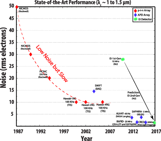
Figure 1. The trend in noise reduction for state-of-the-art SWIR imaging arrays with cutoff wavelength (λc) ~1–1.5 μm over the past 30 years: the equivalent input noise of the ROIC determines the detection limit of the p–i–n detectors and has been nearly constant over the past 20 years. On the other hand, detectors with an internal amplification mechanism, such as the linear-mode avalanche photo diodes can reduce the input ROIC noise. Pixel rate is also indicated in this plot. APD technology allows for significantly higher pixel rates. With Northwestern University’s (NU) first-generation EI detectors and using an off-the-shelf CMOS ROIC with 575–870 electrons rms noise, the measured imager noise was reduced to 28 electrons rms at a frame rate of 1950 frames/s and at 0.5 ms integration time. On-going efforts are for the future development of large-format second-generation EI detector arrays with lower noise. Data obtained from Hodapp (2000), Bai et al. (2004, 2008b), Baker et al. (2004), Destéfanis et al. (2011), McKeag et al. (2011), Finger et al. (2012), Jack et al. (2012), and Feautriera et al. (2015).
Detectors with an internal amplification mechanism, on the other hand, such as the linear-mode APDs can reduce the input ROIC noise. An overall system-level sensitivity enhancement is offered by such a detector compared to p–i–n diodes. The signal-to-noise-ratio (SNR) of the photodetection system utilizing a detector with internal amplification (G) is expressed as , where S is the signal at the input, Namplifier is the preamplifier input noise, and Ndetector is the detector noise (Spieler, 2005). This expression implies that although the noise contribution of the detector is unavoidable, and is always higher than a p–i–n diode, the contribution from the amplifier can be suppressed in the presence of gain in the detector. Another benefit of the internal amplification in APDs is that the arrays can satisfy the significantly increased demands on high pixel rates. Figure 1 illustrates that APD arrays allow for a higher pixel rate compared to p–i–n arrays, and at the same time, they provide a suppressed overall system noise. APD detector arrays with as high as 1-GHz pixel rate have been reported in the literature (Itzler et al., 2011).
Unfortunately, avalanche photodiodes require high bias voltages and are sensitive to material inhomogeneity. As such, to benefit from their advantages in focal plane arrays (FPAs), specifically designed readout circuits capable of applying a high bias and with very low noise are critical. Furthermore, due to a super-exponential gain characteristic, the yield in achieving uniform arrays is low. For example a mere fraction of a percent variation in the epilayer thickness or doping concentration, results in sizeable shifts in the APD output voltage that may render an array unusable (Clark et al., 2006). The large electric field in the device leads to surface breakdown mechanisms and consequently guard rings are required to prevent this phenomenon (Dasgupta et al., 1997). The guard rings increase the pixel pitch and reduce the fill factor. Furthermore, the APD pixels need to be spaced apart to prevent crosstalk due to carrier re-emission. Hence, realization of high-resolution imagers has remained a challenging task for APD based imagers. Recent advances in device design and epitaxial growth have made formation of 256 × 320 pixels and 30 μm pixel pitch APD arrays possible (de Borniol et al., 2010; Rothman et al., 2014). Furthermore, APDs suffer from afterpulsing, which results in long deadtimes (Ribordy et al., 2004), and increases the jitter of the device (Itzler et al., 2007). On the other hand, p–i–n detectors operate at low (CMOS compatible) bias voltages. The electric field in the p–i–n detector active region is less than APDs, and this feature makes p–i–n detectors less sensitive to material inhomogeneities. As shown in Figure 2, the p–i–n imaging focal plane array sizes has increased in proportion to the ability of readout integrated circuit technology to read, process, and demonstrate the detector array signals. Currently, the most advanced sensors are based on the Hawaii-4RG, with 4096 × 4096 pixels and 10 μm pixel pitch (Bai et al., 2008a; Finger et al., 2009).
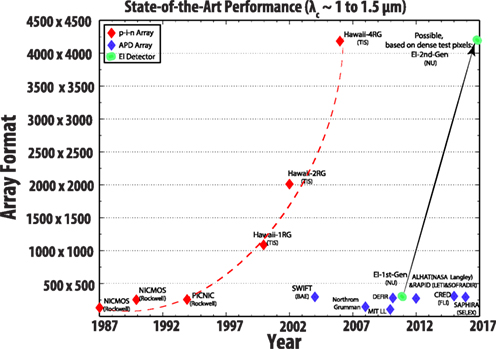
Figure 2. The trend in array size for state-of-the-art SWIR imaging arrays with cutoff wavelength (λc) ~1–1.5 μm over the past 30 years: array format for p–i–n detectors have continued to increase is in proportion to the ability of readout integrated circuit technology to process the detector array signals. For APDs, on the other hand, array size and pixel pitch are limited fundamentally as a result of the high electric fields in the device and the super-exponential gain characteristic of detector with bias voltage. Array size of Northwestern University’s (NU) first-generation EI detectors is also marked in the plot. On-going efforts are currently for the development of large-format EI detector arrays using second-generation EI devices. Data obtained from Hodapp (2000), Bai et al. (2004, 2008b), Baker et al. (2004), Destéfanis et al. (2011), McKeag et al. (2011), Finger et al. (2012), Jack et al. (2012), and Feautriera et al. (2015).
Avalanche photodetectors based on III-V material have another important limitation as well. They exhibit an inherent uncertainty in the multiplication process, which significantly elevates their noise levels (McIntyre, 1966; Lau et al., 2006). They have typical noise factors of F ~ 4–5 (Feautriera et al., 2015). As such, huge amount of work has been reported in the literature to reduce the multiplication noise in such APDs (Saleh et al., 2000; Hayat et al., 2002; Kwon et al., 2003). Mercury Cadmium Telluride (HgCdTe) is the most important semiconductor alloy system for IR detectors in the mid-wave infrared (MWIR) and long-wave infrared (LWIR) spectral range and has addressed this issue. HgCdTe material system can offer an excess noise factor of near unity (Leveque et al., 1993; Vojetta et al., 2012), which is the result of a nearly exclusive impaction ionization of the electrons (Feautriera et al., 2015). APDs based on HgCdTe material system are denoted as “electron initiated APDs or eAPDs.” Unfortunately, in the SWIR region between 1 and 2.5 μm, these detectors do not offer any gain (Rogalski, 2011). For SWIR region, to obtain gain with a near unity excess noise, detectors with a bandgap in MWIR are typically cooled to ~60 K (Rogalski, 2012; Gach and Feautrier, 2015). The extensive cooling is due to the fact that HgCdTe eAPDs utilize a bandgap that is much smaller than what is needed for SWIR detection. Furthermore, low pass filters are utilized to filter out the longer wavelengths (Dhar et al., 2013).
Electron-injection (EI) detectors are an alternative approach to above detection technologies for SWIR band, and are based on an electron-injection process. They utilize the exact band gap required for SWIR detection and, as such, compared to the SWIR HgCdTe eAPD, require much less cooling. Similar to p–i–n diodes, they operate at CMOS compatible bias voltages (Fathipour et al., 2014a). Similar to linear-mode APDs, they provide an internal amplification to suppress the readout noise. On the other hand, unlike APDs, due to an inherent negative feedback inside the device, the amplification mechanism is avalanche-free and stable. Furthermore, they have an excess noise of near unity (Memis et al., 2008a,b; Fathipour et al., 2014b; Fathipour and Mohseni, 2015a). The low electric field in the device (~40 KV/cm) together with a sub-linear gain dependence on the bias voltage makes formation of high yield large-format high pixel density FPAs less challenging with this technology for low photon flux applications. Another benefit of this technology is that it satisfies the significantly increased demands on pixel rates due to increased collection area (as a result of its gain). EI detectors are based on the mature InP material system, and have a cutoff wavelength of 1700 nm.
Electron-injection detectors are similar to phototransistors (Campbell et al., 1981a,b; Lin et al., 2000), but with two distinct differences: a unique 3-D geometry, and a type-II band alignment as we have reported earlier, and will discuss in more detail in this paper (Fathipour et al., 2016). EI detectors operate by absorbing photons in a large volume, confining the photo-excited holes into a small sensor, and then amplifying the signal through electron-injection. Detector output pulse is intrinsically proportional to the number of photons absorbed (Memis et al., 2008b, 2010a; Fathipour et al., 2013a; Fathipour and Mohseni, 2015b). Due to the different charge-carrier multiplication process compared to an APD, EI detectors have typically a lower bandwidth [approximately few nano second rise time at 20 μW optical power at 1550 nm (Movassaghi et al., 2016)]. Nonetheless, detector can achieve a higher theoretical bandwidth, once its structure is optimized. Last but not least, EI detectors utilize a less expensive material system compared to HgCdTe APDs, as InP foundries are available.
This review aims to act as an introduction to the principle of operation of the electron-injection detectors, their design, layer structure, status, and future directions. It provides a broad overview to their characteristics including optical gain, dark current, and response time. Detectors were demonstrated for the first time in 2007, and have been fabricated and tested during two generations of development and optimization cycles. First-generation detectors yielded large dark currents with a limited bandwidth of ~3 KHz. The low bandwidth and large dark current limited the application of first-generation devices in many fields. A prototype 320 × 256 pixel and 30-μm pixel pitch EI imager was demonstrated in 2010. An off-the-shelf CMOS ROIC with 575–870 electrons rms noise was utilized for hybridization. As a result of the internal charge amplification mechanism in the detector, the measured imager noise was reduced to 28 electrons rms at a frame rate of 1950 frames/s. The results of the fist generation devices are indicated by green markers in Figures 1 and 2.
The shortcomings of the first-generation devices were addressed in the second-generation detectors. Second-generation devices achieved high gain, high bandwidth, and low leakage current in a single structure at room temperature. Compared with first-generation detectors, the second-generation devices achieved two orders of magnitude lower dark current and four orders of magnitude enhancement in bandwidth. We demonstrate the first and the second-generation results. We compare the second-generation of detectors with first-generation devices, as well as the best-reported linear-mode APD, which is based on HgCdTe. We demonstrate a performance comparison with other SWIR detector technologies with internal amplification in terms of noise-equivalent sensitivity. Finally, we illustrate the benefit of scaling of the injector diameter with respect to the trapping/absorbing layer diameter using an analytical model and confirm it by experimental data. We discuss future development of large-format EI detector arrays based on second-generation of devices (also shown using arrows in Figures 1 and 2). These improvements have opened up applications for these detectors in medical field (optical coherence tomography), remote sensing (light detection and ranging), and astronomy (exoplanet detection). These are the focus of our current research.
Electron-Injection Detector Layer Structure
The schematic diagram of the detector together with the energy band diagram as a function of depth along the central axis of the device, in darkness (blue), and under illumination (red) are shown in Figures 3A,B, respectively. Detectors have a type-II band alignment. The layer structure consists of 1000 nm n− doped (<1015 cm−3) In0.53Ga0.47 absorber, 50 nm p+ doped (5 × 1018 cm−3) GaAs0.52Sb0.48 hole trap (electron barrier), 50 nm undoped In0.52Al0.48As etch stop, 500 nm n+ doped (1017 cm−3) InP injector, and 50 nm n+ doped (1019 cm−3) In0.53Ga0.47As cap layer. The epitaxial layers are grown with metal organic chemical vapor deposition (MOCVD) on 2″ InP substrates (Fathipour et al., 2014).
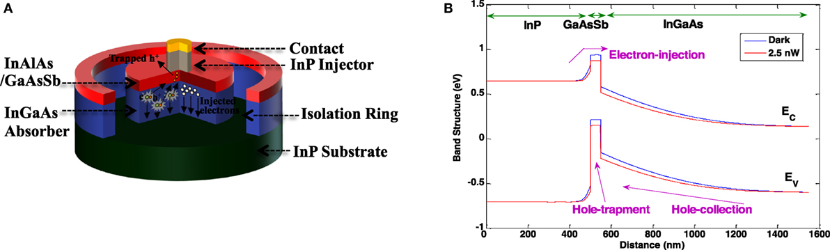
Figure 3. (A) The schematic diagram with a cross section showing the operation mechanism (B) the band diagram through the central axis as a function of depth: in darkness (blue), and under illumination (red) for an electron-injection detector. The InAlAs layer is not included in (B).
Detection Mechanism
Due to the doping level of each layer, an internal electric field exists in the InGaAs absorber (Figure 3B), which gets stronger when the device is biased correctly.
Photon absorption results in generation of an electron–hole pair in the InGaAs absorber. The large volume of the absorber ensures that the incoming photons are captured with high efficiency. Under negative bias, the electron and the hole are separated. The injector is responsible for altering the potential of the GaAsSb layer such that the minimum potential for holes will be formed in the GaAsSb region under the injector. As a result, the hole gets trapped in the GaAsSb trap layer for the period of its lifetime. This leads to a change of barrier potential, and results in a large electron injection, and hence internal amplification in the device. As the electrons pass over the barrier, they lower the local potential and increase the barrier height, opposing the flow of more electrons. This negative feedback mechanism results in a stable low noise internal amplification, and an excess noise factor of unity (Memis et al., 2008b). The trapped hole finally recombines with an electron, relaxing the bands (Fathipour et al., 2013b).
As shown in Movassaghi et al. (2016), the charging rate of the GaAsSb trapping layer by electrons (and the neutralizing holes) is ultimately limited by the minority-electron lifetime in the GaAsSb layer (τe). The ultimate bandwidth of device is thus dictated by the electron lifetime in the GaAsSb layer. The ratio of the minority-electron lifetime in the GaAsSb layer to electron transit time (τB) dictates the ultimate device gain. As such, the ultimate gain-bandwidth product of the device is dictated by the GaAsSb trapping layer transit time.
Fabrication Process
Electron-injection detectors are fabricated by patterning the wafers with photo (e-beam) lithography to form the contact metals. E-beam lithography is used for formation of submicron injectors (contacts). Conventional metallization with an e-beam evaporator is used to lift off multi-layer metal contacts, which act as hard mask for reactive ion etching with methane-hydrogen (CH4/H2) chemistry to form the injector pillars. This etch selectively etches InP and InGaAs versus InAlAs.
In the second-generation of electron-injection detectors an absorber diameter of 30 μm is obtained by physically etching the active region. To form the isolating trenches, wafers are patterned by photolithography. This is followed by utilization of two selective wet etches and one dry etch with a high verticality. The first etch is HCl:H3PO4:H2O (16:7:4) at 5°C, which selectively etches InP (&InAlAs) versus InGaAs/GaAsSb (Bhat et al., 1996). The second selective etch removes InGaAs (&GaAsSb) versus InP (Stano, 1987). It consists of H2SO4:H2O2:H2O (10:1:1) cooled at 5°C. To etch InGaAs absorber, we used methane-hydrogen dry etch. The dry etching recipe is optimized to obtain minimum surface and sidewall damage for detector mesas.
The SEM image of an electron-injection detector with 30 μm diameter absorber and 10 μm diameter injector is shown in Figure 4A. Figure 4B is a cross sectional SEM image of the device and the inset shows a zoomed SEM image of the InP injector, InAlAs etch stop/GaAsSb trapping layer and part of InGaAs absorber. The dielectric in Figure 4B is silicon on glass, which is used for planarization purposes. The schematic diagram of fabrication process is shown in Figure 4C.
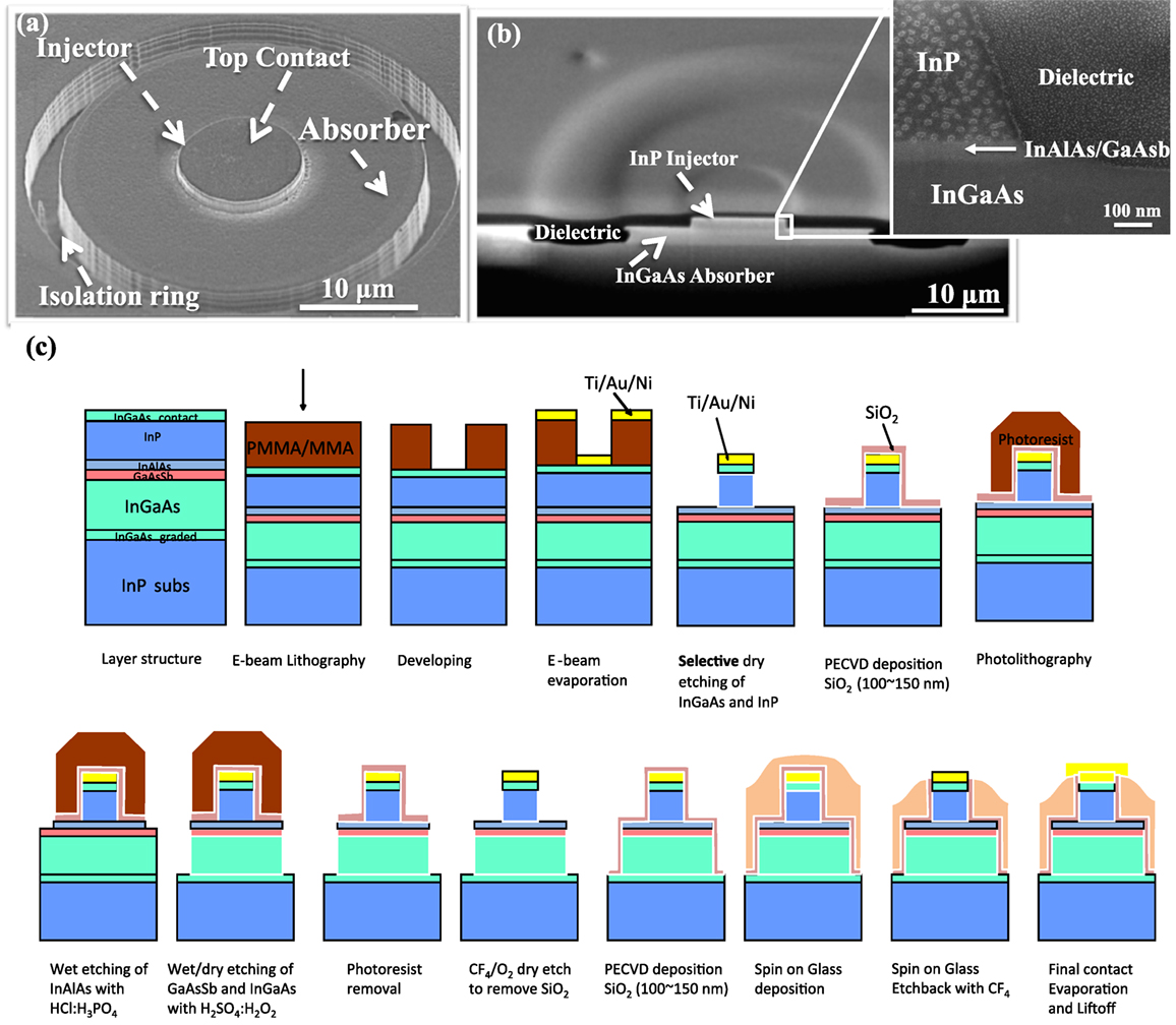
Figure 4. (A) SEM image of a second-generation electron-injection detector with 30 μm diameter absorber and 10 μm diameter injector. (B) A cross sectional SEM of the device through its center. Detector is planarized by a dielectric material (Silicon on Glass). Inset shows a zoomed SEM of InP injector, GaAsSb trapping layer/InAlAs etch stop and part of InGaAs absorber. (C) Schematic diagram of process flow. Reproduced with permission from Fathipour et al. (2015). Copyright 2015 AIP Publishing LLC.
Besides device isolation, in the second-generation devices, contact resistance was minimized through removal of surface oxides and an organic-free all dielectric lift-off process. Low contact resistance is inevitably required for any high-speed device. Due to the inherent high gain and the small contact size in the electron-injection detector, having a poor contact resistance can be detrimental in the device pulse response. The utilized high-speed voltage preamplifier in our measurements has a nominal input impedance of 50 Ω, and any comparable contact resistance will drop the voltage seen on the preamplifier. For example, a contact resistance of 100 Ω, which is negligible compared to the device impedance, can drop the voltage to a third of what it should be. In parallel, it would increase the RC time constant in the pre-amplification loop slowing the device response. A good contact requires sharpest and cleanest lift-off patterns. Patterned resists commonly leave small traces of resistive organics on the surface. This residue is extremely problematic in submicron contacts as it can result in contact resistivity to become noticeably larger. We developed an organic-free quad layer lift-off pattern with 250 nm SiO2/100 nm SiN/5 nm SiO2/PMMA for e-beam or 250 nm SiO2/100 nm SiN/5 nm SiO2/Photoresist for photolithography. After patterning and development, this dielectric layer stack can be dry etched by CF4 plasma followed by buffered oxide etch to form undercut (Figure 5). This process prevents any organic residue on the semiconductor surface, while forming a reliable negative profile for thick metal evaporation.
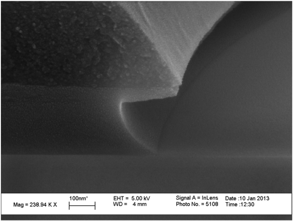
Figure 5. SEM images of the organic-free quad layer lift-off pattern with SiO2/SiN/SiO2/Photoresist stack ready for thick metal evaporation.
To remove surface oxides, a short surface treatment with ammonium hydroxide was used followed by Ti/Au/Ni evaporation of contact metals. The ammonium hydroxide was responsible for removing the surface oxides and any parasitic series capacitances (i.e., due to native oxide/organics on semiconductor); however, it also attacked the resists, so the treatment time was kept short at 10–15 s. In the second-generation devices the contact resistance was measured using 40 μm × 10 μm TLM patterns. The resulting contact resistivity was 2 × 10⁻⁵ Ω cm2. Above contact resistivity was limited by the resistance of our measurement system. Furthermore, due to the size difference between large TLM patterns and the electron-injectors contacts, above resistivity might not be necessarily the same for the electron-injection contacts.
Electron-Injection Detector Results
First-Generation Results
First-generation of electron-injection detectors were not isolated from each other (Figure 6A). The injector diameter was 10 μm. These detectors showed a large stable gain of ~6,802 (Memis et al., 2008a) and a dark current of 6 μA at −1.5 V bias (Figure 6B). Furthermore, these devices yielded a low bandwidth of ~3 KHz. The optical gain of 6802 corresponds to a responsivity of 3762 A/W at 1550 nm wavelength. When devices were passivated, the active area of the detector increased to beyond 100 μm by 100 μm, and their bandwidth increased, but they suffered from a reduced optical gain of ~2–5. The jitter of the passivated detectors was measured to be ~14 ps at room temperature (Memis et al., 2008a).
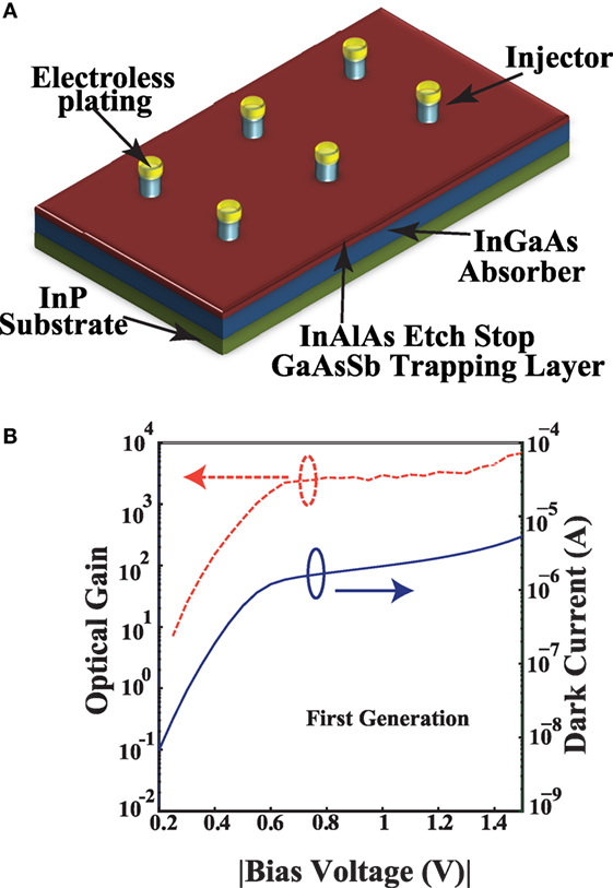
Figure 6. (A) Schematic diagram of first-generation of electron-injection detectors. (B) Plots of electron-injection detector characteristics: dark current and optical gain versus bias voltage characteristic at room temperature. Detectors have 10-μm injector diameters. Please note that a negative bias is applied to the injector and (B) shows the magnitude of bias voltage.
To form an infrared camera (Memis et al., 2010a), after characterization of individual electron-injection detectors, 320 by 240 pixel arrays of detectors were formed with 30-μm pixel pitch. The FPA common plane was connected to the backside contacts through the highly doped graded layer of InGaAs, which is at the interface of InP substrate and the InGaAs absorber. Figure 7A shows an optical microscope image of the FPA, the detector common hybridization ring and alignment marks. Indium bump bonding was used to hybridize the detector array with off-the-shelf silicon CMOS readout integrated circuit, ISC9705 from Indigo. Scanning electron microscope images of the indium plated FPA, with 30-μm pixel pitch is shown in Figure 7B. Figure 7C illustrates the hybridized electron-injection imager placed on a leadless chip carrier (LCC) and wire bonded. Figure 7D shows the camera, which contains a vacuum dewar for cooling of the LCC, and also houses the controlling electronics.
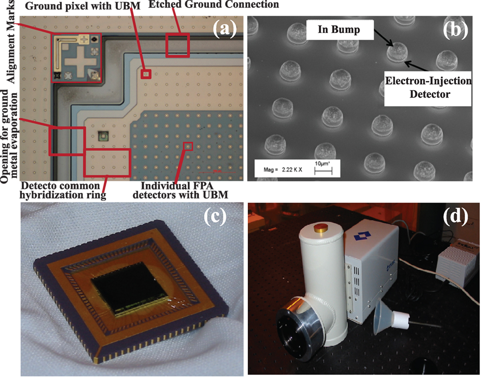
Figure 7. (A) Optical Microscope image of electron-injection imager showing the focal plane array, the detector common hybridization ring, Under-Bump-Metallurgy (UBM) for Indium plating and alignment marks. (B) SEM image of the detectors with indium bumps on top ready for integration (Memis et al., 2010b) (C) A picture of the final electron-injection imager on a leadless chip carrier (D) A picture of the infrared camera housing. Reproduced with permission from Memis et al. (2010a).
The electron-injection camera was compared with a commercial SWIR camera (AlphaNIR from FLIR). The rms noise level of the (ISC9705) CMOS ROIC was 575–870 electrons. The readout noise of electronics in the commercial camera from FLIR was more than 10 times smaller than our readout noise (50 electron noise rms). The integration time was set to 0.5 ms and f/1.8 lenses were used for both cameras. The dynamic range of both cameras was equalized by disabling the auto gain and contrast in both cameras while they were imaging the same scene. FLIR camera has the same pixel size and resolution as the electron-injection imager and was internally thermoelectric (TE) cooled (to its optimal operating temperature of −7°C). The electron-injection imager was placed in an evaluation kit from Indigo, and was cooled to −7°C and −75°C. Besides the visual comparison of the cameras in a low-light-level scene (Figure 8A), we measured the SNR histograms of the two cameras (Figure 8B), as well as the absolute SNR of our camera (Figure 8C).
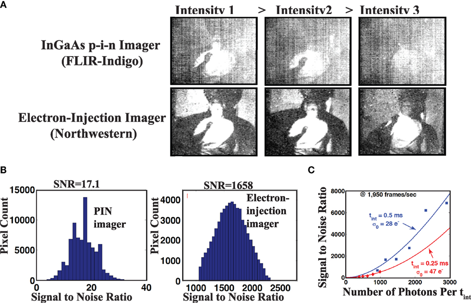
Figure 8. (A) Comparison images of a commercial camera (AlphaNIR, from FLIR) and the first-generation electron-injection imager. Both cameras are cooled, coupled with f/1.8 lens, and used at the same integration time of 0.5 ms. (B) The SNR histograms of the commercial AlphaNIR camera (left) and the first-generation electron-injection imager (center), acquired by imaging the same source at equal dynamic range. (C) The plot of the SNR versus the number of photons per integration time of the first-generation electron-injection imager. The data was fitted to the theoretical equation, and the noise parameters were extracted from the fit (Memis et al., 2010a).
First, the images of a calibrated, uniform, and adjustable light source were acquired with both cameras for comparison. The ratio of the signal squared to standard deviation squared yielded the SNR for each pixel. Signal was calculated from the subtraction of the dark from the illuminated scene, and standard deviation of each pixel was calculated from its time evolution.
At −7°C, 11% SNR improvement was achieved for the electron-injection imager compared with the AlphaNIR. Under further cooling, the p–i–n based FLIR camera became limited by the temperature independent ROIC noise level and did not offer improved SNR. However, cooling the electron-injection detector to −75°C, resulted in improvement of SNR by two orders of magnitude compared with the commercial SWIR camera (1656 versus 17.1) (Figure 8B). This is the result of the internal amplification in the electron-injection imager (Memis et al., 2010a).
Second, a NIST calibrated laser at 1.55 μm was focused onto the electron-injection camera, and images were acquired. The measured data was fitted to the SNR expression (Personick, 2013) to obtain the excess noise factor and the overall pixel noise (Memis et al., 2010b):
where , Φ is photon flux/second, tint is the integration time, G is the detector internal amplification, F is the excess noise factor, σ is the noise, N is the number of photons, σ′ is the overall input noise of the system, Popt is the calibrated optical power, and Eph is the photon energy.
As shown in Figure 8C, at an integration time of 0.5 ms and a frame rate of 1,950 frames/s, the SNR analysis revealed that the overall noise of the imager was 28 electrons rms. This was much less than our nominal read-out noise of 575–870 electrons rms. More importantly, the imager excess noise was about unity. When the integration time (tint) was halved, the noise almost doubled (at about 47 e− rms), in agreement with the expected inverse scaling with integration time (Saleh et al., 1990). The large dark current of the first-generation detectors prevented longer integration times. However, extrapolating the integration time shows that an overall noise of less than 2 e− at tint = 10 ms (100 frames/s) is achievable (Memis et al., 2010b).
The limitation of the first-generation of electron-injection detectors was that they could only achieve high gain performance at very low bandwidths. Furthermore, these devices suffered from high leakage currents. We have addressed these challenges in the second-generation electron-injection detectors, which simultaneously achieve high gain, high bandwidth, low jitter, and low dark current in a single structure. These improvements have opened up application for these devices in a variety of fields.
Second-Generation Results
Our experimental studies as well as simulation results (Fathipour et al., 2014; Movassaghi et al., 2016) demonstrated that in order to achieve very low dark current and fast response time, in a single device, it is necessary to physically separate individual pixels. This results in a pre-defined active area for each detector and allows the charge localization dynamics to be accurately controlled with the active area of each detector.
In this section, we report the experimentally measured characteristics of the second-generation electron-injection detectors, which have physically isolated individual pixels, and compare them with those of the first-generation devices. Here, we compare devices with same size injector diameter (10 μm) for both generations. The second-generation electron-injection detector has further been compared with the state-of-the-art semiconductor technology [SWIR HgCdTe eAPD (Foubert et al., 2013)] in terms of dark current density. We demonstrate a performance comparison with other SWIR detector technologies with internal amplification and show that the electron-injection detectors offer more than three orders of magnitude better noise-equivalent sensitivity compared with state-of-the-art phototransistors operating at similar temperature. Finally, we demonstrate the reason for scaling the injector diameter with respect to the trapping/absorbing layer diameters.
Dark Current and Gain Characteristics
Figure 9A shows schematic diagram of an array of second- generation isolated electron-injection detectors, and Figure 9B plots the measured dark current and optical gain characteristic. The isolated electron-injection detectors achieve more than two orders of magnitude lower dark current compared with the first- generation and sustain the high internal amplification. At −3 V bias voltage, the gain is measured as approximately ~3000 and the dark current is ~10 nA.
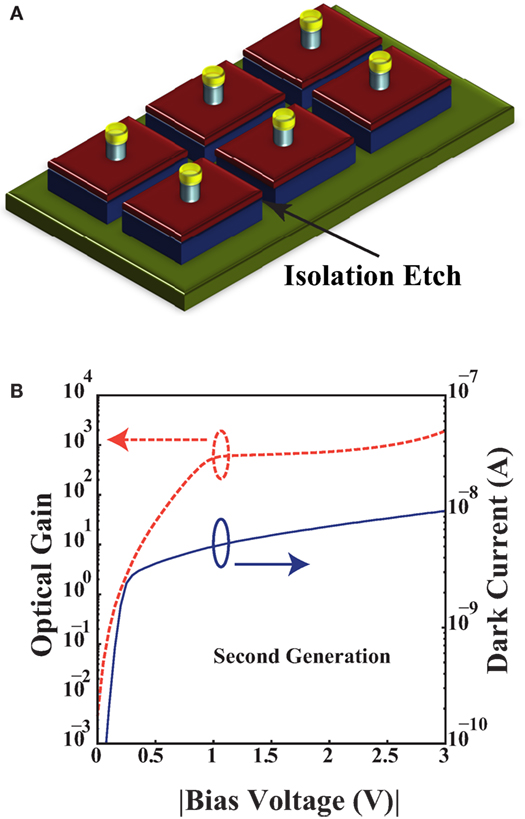
Figure 9. (A) Schematic diagram of second-generation of electron-injection detectors. (B) Plots of second-generation electron-injection detector characteristics in log scales: dark current and optical gain versus bias voltage characteristic at room temperature. Detectors have 10 μm injector diameters and 30 μm absorber diameters. Please note that a negative bias is applied to the injector and (B) shows the magnitude of bias voltage (Fathipour et al., 2013b).
To measure the detector optical gain, a continues-wave monochromatic source at 1550 nm central wavelength illuminated the device from the topside. The beam was focused beside the injector using a microscope setup, to a spot of approximately 3 μm in diameter. The detector photo current was amplified using a trans-impedance amplifier, which also provided the device bias. Laser power was calibrated using a NIST calibrated p–i–n detector. Using the data from calibrated photocurrent and dark current measurements, the responsivity (R) and consequently the optical gain were extracted. Responsivity in an electron-injection detector is the composite of the internal quantum efficiency (ηint) and the internal gain (M) and it can be difficult to separate the two by a measurement technique (Fathipour et al., 2016):
In Eq. 2, q is the electric charge, and Eph is the photon energy. Here, we equate the internal quantum efficiency to 100% and underestimate the internal gain. The external quantum efficiency (ηext) was calculated from the uncoated surface reflectivity (r ~ 30%), the thickness of the absorbing layer (L ~ 1 μm) and its absorption coefficient (α ~ 1 μm−1 at 1550 nm).
Temperature Dependence of Dark Current
Figure 10A is a logarithmic plot of dark current versus bias voltage for temperatures ranging from 300 to 160 K. For temperatures below 160 K, the leakage current of our measurement setup dominates the measured current.
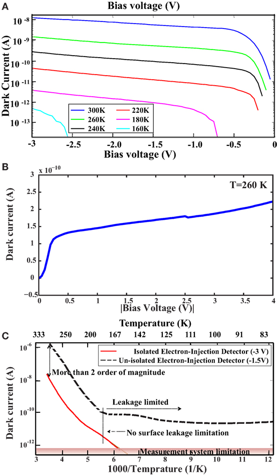
Figure 10. (A) Logarithmic plot of dark current versus bias voltage at different temperatures. (B) Dark current versus bias characteristic at 260 K. Please note that a negative bias is applied to the injector with respect to the backside substrate and (B) shows the magnitude of bias voltage. (C) Arrhenius comparison of the dark current of an isolated electron-injection detector with 10 μm injector and 30 μm absorber diameter (at −3 V bias) with our previously reported result of un-isolated devices with 10 μm injector (at −1.5 V bias). More than two orders of magnitude reduction in dark current is achieved. Furthermore, in the isolated detectors, no sign of temperature independent dark current was observed below 175 K, down to 160 K (Fathipour et al., 2013b, 2014b).
Figure 10B shows the dark current characteristic of an isolated electron-injection detector (linear scale) at a temperature of 260 K. The sub-linear dependence of dark current on bias voltage is an advantage for the electron-injection detector when compared with APDs/eAPDs, in which the dark current raises exponentially with bias voltage. As a result, when utilized in large format FPAs, the electron-injection detector gain does not vary much by the voltage and process variations across the FPA.
Figure 10C compares the dark current as a function of temperature for the first and the second-generation detectors (Memis et al., 2010a; Fathipour et al., 2014,b). It is illustrated that the second-generation detector provides more than two orders of magnitudes reduction of the dark current at any temperature. Furthermore, no sign of surface leakage limited dark current, which would result in a significant change in the slope of the plot, is observed (Memis et al., 2010a).
Rise Time and Jitter
To evaluate the speed of response of the isolated devices, a pulsed laser, with ~3 ns rise time, at 1550 nm central wavelength was used. Detectors were biased at −3 V, using a DC power supply fed through a bias-tee. The RF signal coming from the device was extracted using the bias-tee and amplified by our low noise voltage amplifier with 1.1 GHz nominal bandwidth. The amplified signal was then acquired by a high-speed oscilloscope (2.5 GHz bandwidth). The devices exhibited a 10–90% rise time of ~6 ns at 40 μW optical power. The pulse response is shown in Figure 11.
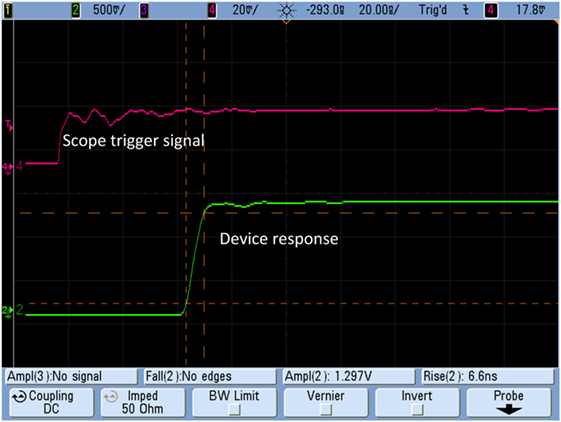
Figure 11. Detector pulse response at −3 V bias voltage: showing 6.6 ns rise time.
As mentioned in “Detection Mechanism” section it is worth noting that due to the feedback stabilized gain mechanism, electron-injection detectors do not suffer from afterpulsing and their ultimate bandwidth is limited by minority-carrier lifetime in the GaAsSb layer (~1–10 ns reported in the literature) (Movassaghi et al., 2016).
To measure the jitter, a femtosecond pulsed laser with <70 fs jitter was attenuated and focused onto the detector. The RF signal coming from the device was extracted using the bias-tee. The amplified signal was then acquired by a high-speed sampling oscilloscope, Agilent 86100C (jitter: 1.7 ps), which directly measured jitter. The timing signal was generated by a low-jitter (1.2 ps) p–i–n detector connected to the second output port of the laser. Jitter of 12 ps at room temperature was measured for second-generation of devices at optical powers ~ >10 uW.
Comparison with the State-of-the-Art Semiconductor Technology
Figure 12 compares the temperature dependence of the dark current density of the second-generation electron-injection detector and the best-reported SWIR HgCdTe eAPD(λc ~ 3 μm) (Vojetta et al., 2012; Foubert et al., 2013). As shown in this figure, the dark current density of the isolated electron-injection detector is close to two orders of magnitude lower than the HgCdTe eAPD.
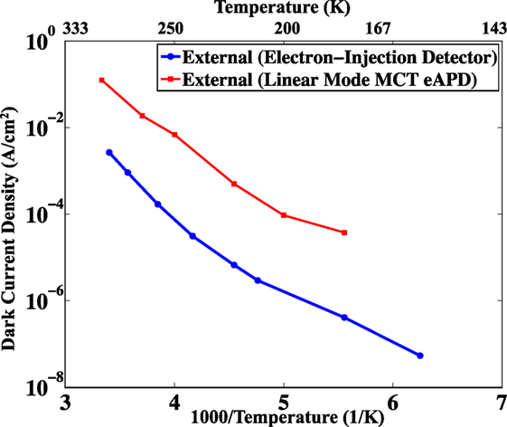
Figure 12. Temperature dependence of the dark current density of the best-reported SWIR HgCdTe eAPD (Vojetta et al., 2012; Foubert et al., 2013) and the electron-injection detector: electron-injection detector has more than an order of magnitude lower dark current density (Fathipour et al., 2014b).
Comparison with SWIR APDs and HPTs in Terms of Noise-Equivalent Sensitivity
Electron-injection detectors have been compared in terms of noise-equivalent sensitivity to a number of APDs, and heterojunction phototransistors (HPTs) in Fathipour et al. (2016). Figure 13 plots the measured SNR at 260 K. The black line represents the maximum achievable signal-to-noise-ratio (SNRsh), which is dictated by the statistical nature of incoming photons: , where BW is the measurement bandwidth (limited by our trans-impedance amplifier bandwidth ~100 KHz), PRF is pulse repetition frequency (50 KHz), F is the excess noise factor (unity), and η is the total quantum efficiency. The electronic noise of the amplifier was measured to be 2600 electrons rms in a 10 μs laser pulse. The green solid curve shows SNR of a detector with zero dark current, same quantum efficiency as the electron-injection detector, and no internal amplification (such as an ideal p–i–n detector). As shown in this figure, the ideal p–i–n detector requires at least 5806 photons to achieve a unity SNR. On the other hand, the electron-injection detector achieves noise-equivalent sensitivity of ~670 photons in a 10 μs laser pulse. Thus, the contribution from the amplifier noise (~2,600 electrons rms) is suppressed in the presence of the gain in the EI detector. Our sensitivity is still limited by the amplifier noise, and better amplifiers – such as ones used by others in similar measurements – (Vojetta et al., 2012; Foubert et al., 2013), could lead to better results with the current devices. Our model shows that under the condition of suppression of the injector/trapping layer recombination current, (as explained in the next section) such that an amplification of ~3000 for the EI detector is maintained at all photon numbers, one can achieve a noise-equivalent sensitivity of 25 photon (limited by dark current) at 260 K with the current amplifier. This is shown by the red curve in Figure 13. For comparison purposes, the measured noise-equivalent sensitivity of a number of SWIR APDs and HPTs reported in the literature is also included in this plot. Black markers show room temperature data and red markers show data at similar temperature (260 K). Here, we took the conservative approach of equating external quantum efficiency of all detectors to 100% unless otherwise stated in the reference. The corresponding value for EI detector was ~44%. As shown in this plot, HPTs typically show a larger value of noise-equivalent sensitivity compared to APDs. The EI detector technology achieves a better performance compared to both technologies. Our theoretical calculations confirm the measurement data.
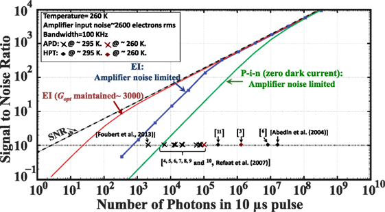
Figure 13. The minimum number of photons that the EI detector can detect (~670 photons) is limited by the electronic noise from the post-detection circuitry amplifier noise (~2600 electrons root mean squared in 10 μs pulse width). Performance comparison with other SWIR detector technologies demonstrated that the electron-injection detectors offer more than three orders of magnitude better noise-equivalent sensitivity compared with state-of-the-art phototransistors operating at similar temperature (Fathipour et al., 2016). Data available in3–11, Abedin et al. (2004), and Refaat et al. (2007).
Impact of the Unique Three-Dimensional Geometry on the Performance of Electron-injection Detectors
In this section, we present a quantitative study of the influence of three-dimensional geometry of the isolated electron-injection detectors on their characteristics. Analytical expressions are derived for the electron-injection detector optical gain to qualitatively explain the significance of scaling the injector with respect to the trapping/absorbing layers. Detailed information of the effect of scaling the injector with respect to absorber on rise time, dark current and gain can be found from Movassaghi et al. (2016). Devices with about ten times smaller injector area with respect to the trapping/absorbing layer areas show more than an order of magnitude lower dark current, as well as an order of magnitude higher optical gain compared with devices of same size injector and trapping/absorbing layer areas.
To study the impact of scaling of the injector with respect to the trapping/absorbing layer areas, two types of detector geometries were fabricated: type A detectors have mesa structures with equal trapping/absorbing layer diameter (d1) and injector diameter (d2) and type B detectors have a smaller injector diameter compared with the trapping/absorbing layer diameter (Figure 14). Different sizes of both detector types were fabricated. For type A detectors, d1 = d2 varied between 274, 174, 123, 82, and 33 μm, and for type B detectors, injector diameter was 10 μm and the trapping/absorbing layer diameter was 30 μm. Our current probing method for electrical measurements does not allow reliable results for contact diameters below 10 μm.
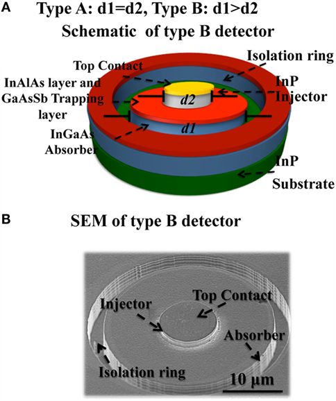
Figure 14. (A) Schematic diagram and (B) SEM of type B electron-injection detector with 10 μm injector diameter and 30 μm absorber diameter. d1 and d2 refer to the trapping/absorbing layer and injector diameters respectively. Reproduced with permission from Fathipour et al. (2015). Copyright 2015 AIP Publishing LLC.
Figure 15A shows the measured dark current versus bias voltage characteristic for type A and type B devices at room temperature. To obtain statistically correct data, for each detector type, dark current of an average number of 10 devices was measured per device size. Dark current of type A detectors with mesa sizes ≥80 μm scales proportional with the device area and follows the expected sub-linear relation with bias voltage. Dark current of the scaled injector type B device is an order of magnitude lower than that of a type A device with a similar mesa size (33 μm mesa).
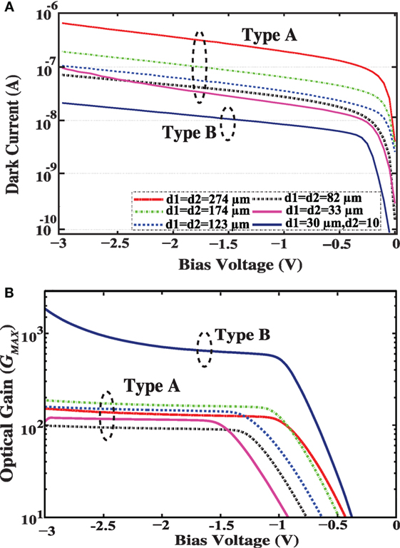
Figure 15. (A) Measured electron-injection detector dark current versus bias voltage characteristic. Data were obtained by averaging over 10 detectors per device size. (B) Measured optical gain (GMAX) versus bias voltage characteristic. Color-coding for part (A,B) is the same. Reproduced with permission from Fathipour et al. (2015). Copyright 2015 AIP Publishing LLC.
Figure 15B shows the extracted optical gain (GMAX) versus bias voltage for type A and type B devices at room temperature. Optical gain increases with bias at small negative bias voltages, and beyond bias voltage of ~−1.5 V, a stable gain of ~100 for type A devices and ~2000 for type B device is achieved. From Figures 15A,B, one can conclude that the internal dark current densities (obtained by dividing the external dark current densities by the optical gain) of all device structures have similar values with the exception of the smallest mesa type A device, which may possibly be dominated by surface effects. The surface effects seem to be not very significant despite the rather large exposed surfaces in the type B devices.
Optical gain was measured at room temperature for various incident optical power levels in both types of detectors. The corresponding plot of the measured optical gain versus the photogenerated current density at −3 V bias voltage is shown in Figure 16. Optically generated holes are trapped in the GaAsSb trapping layer, and their accumulation causes an increase in the forward bias voltage (VBE) of the injector/trapping layer heterojunction. To derive an analytical expression for the optical gain, the device is assumed to be operating in the forward operation regime. Both the photogenerated current, Igen, and the resulting amplified photo current injected from the injector into the absorber, Iamp-photo, are driven by the forward bias voltage (Lin et al., 2000):
where is the saturation current injected to the absorber, ISS is the saturation current for recombination in the undepleted part of GaAsSb layer, and ISE is the saturation current for recombination in injector/trapping layer space charge region primarily at low optical power levels. This current is more significant than ISS and is usually large in heterojunction devices due to the strong and dominant recombination in the base emitter space charge region (Campbell and Ogawa, 1982; Chandrasekhar et al., 1991; Lin et al., 2000; Tan et al., 2004; Park et al., 2010). As we shall see shortly, scaling of the injector with respect to the trapping layer reduces this recombination current ideally by the ratio of trapping layer to injector area (AB/AE). The factor represents the ratio of (hole) minority carrier injection to InP, to (electron) majority carrier injection to GaAsSb. In the expression for γ−1, Dn and Dp are the minority carrier diffusion coefficients in GaAsSb and InP layers, Wp and Wn are the respective layer thicknesses, and NpA and NnD are the doping concentrations (acceptor and donor, respectively). Furthermore, , and are the effective masses of electron and hole in GaAsSb and InP layers, and Egp and Egn are the relative bandgap energies. In the expression for IS, niP is the GaAsSb intrinsic carrier concentration, and ηF and ηE are the injector and trapping layer current ideality factors. Using published experimental parameters given in http://www.ioffe.ru/SVA/NSM/, Maneux et al. (2005), and Iverson et al. (2014), we find γ = 2.95 × 10¹⁰. Under large optical power levels (tens of microwatts), optical gain, which is the ratio of Iamp-photo to Igen has maximum value of and its value can be read from measurement data of Figure 15B or Figure 16.
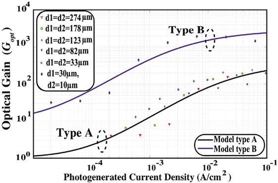
Figure 16. Optical gain as a function of the photogenerated current density at −3 V bias voltage: markers show the measured data and the solid lines show our developed analytical model. Reproduced with permission from Fathipour et al. (2015). Copyright 2015 AIP Publishing LLC.
Using GMAX in Eqs 3 and 4, optical gain can be expressed as:
where IS = ABJS and ISE = AEJSE. Assuming that the effective cross section of saturation current IS is related to the base area AB, we get a good fit to our measurement data. Using above equation, curves were fitted to measurement data for type A and type B devices (Figure 16). The corresponding values used to obtain the curves are presented in Table 1, where the first three rows show the constants, and the last three rows show the fitting parameters. Although the epitaxial structures are the same, the slight difference in the value of JS for type A and type B devices might be the result of possible variation in the epitaxial growth (e.g., actual doping levels, thicknesses, and compositions). Furthermore, it has been assumed that the recombination current in depletion region dominates the surface/defect components in the injector/trap heterojunction, i.e., ηE = 2. Measurement data together with Eq. 5 suggest both higher optical gain and lower photogenerated current density for the gain drop in the type B devices. These are possibly the result of a reduced recombination current in the injector/trap depletion region of a scaled injector device. Similar behavior has also been observed in heterojunction bipolar phototransistors (Park et al., 2010). A common issue with heterojunction phototransistors is the reduction of gain at low optical powers. The gain in such devices drops to half of its peak value at photogenerated current density values of ~100–10−2 Acm−2 (Campbell et al., 1981a,b; Lin et al., 2000), which is similar to the measured values in the type A devices. However, this value is pushed back by at least one order of magnitude in the type B devices (Figure 16). Our model together with the measurement results suggest that scaling of the emitter with respect to the base in such devices could possibly address this issue. This improvement may be further enhanced with smaller AE/AB ratio.
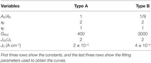
Table 1. Values used in plot of Figure 16.
Conclusion and Future Directions
We have developed a detector that utilizes a noise-free amplification mechanism in an unconventional non-planar topology to boost the signal-to-noise-ratio. The detector, called the electron-injection detector, couples a large, thick absorber with a small sensory injector to sense and amplify the signal. The amplification method is inherently low noise, and the devices show an excess noise of unity. Detectors can be formed into large format high pixel density FPAs with high yield for low photon flux applications.
With the first-generation of detectors, a 320 × 256 pixel imager was demonstrated. The imager provided two orders of magnitude higher signal-to-noise ratio compared to a commercial short-wave infrared imager. The first-generation electron-injection detectors were plagued with high dark current (6 μA at −1.5 V) and low bandwidth (3 KHz). They demonstrated stable signal amplification with gain values exceeding ~2000. The large dark current and slow response time limited their application in many fields.
The second-generation of detectors were designed to get beyond these limitations while retaining the high gain and the unity excess noise factor. Compared to our previous reports, isolated detectors achieved more than two orders of magnitude reduction in dark current and more than four orders of magnitude reduction in rise time. Concurrent high gain (more than ~1000) and high-speed response ~6 ns at optical power levels higher than 10 nW, low leakage (~10 nA), unity excess noise, and low jitter (~12 ps) were measured at room temperature for the second-generation devices at a low bias voltage of −3 V. The gain-bandwidth product approaches tens of giga hertz at optical power levels higher than 10 nW. These characteristics are very difficult to achieve in conventional SWIR detectors at room temperature. The detectors were further compared with the state-of-the-art infrared detector, the best-reported linear-mode SWIR HgCdTe eAPD. Electron-injection detectors showed close to two orders of magnitude lower dark current density at all measured temperatures. Through a detailed experimental measurement and theoretical modeling, we demonstrated the importance of scaling the injector with respect to the absorber.
The improvement in material growth, fabrication, and device design resulted in excellent performance in the second generation of electron-injection detectors compared with the fist-generation. We are currently developing 320 × 256 pixel with 30-μm pixel pitch camera using the second-generation electron-injection detector FPAs. Ultimately, this camera promises to impact astronomy, medical imaging (e.g., deep tissue optical coherence tomography), 3D imaging (e.g., light detection and ranging for self-driving vehicles) and photon-number resolving (e.g., for scalable quantum computing).
While the 320 × 256 arrays find diverse scientific applications, our ultimate emphasis is on the development of ultra-low noise, high pixel density, and larger format camera. On-going efforts are for the future development of large-format EI detector arrays with 4K × 4K readout chips, such as the Hawaii SWIR chips that are already designed to be compatible with p–i–n detectors.
Author Contributions
VF wrote the paper with contributions from all authors.
Conflict of Interest Statement
The authors declare that the research was conducted in the absence of any commercial or financial relationships that could be construed as a potential conflict of interest.
Funding
Authors would like to acknowledge partial support from NSF Award No. ECCS-1310620, ARO Award No. W911NF-13-1-0485, ARO Award No. W911NF-11-1-0390, ARO Award No. W911NF-12-1-0324. Authors would like to also acknowledge the use of Argonne National Laboratory Center for Nanoscale Materials. Use of the Center for Nanoscale Materials was supported by the U. S. Department of Energy, Office of Science, Office of Basic Energy Sciences, under Contract No. DE-AC02-06CH11357. VF would like to acknowledge Ryan Fellowship support.
Footnotes
- ^http://www.sensorsinc.com/applications/spectroscopy/swir-spectroscopy
- ^OSI Optics Product. Available at: http://www.osioptoelectronics.com/application-notes/AN-Photodiode-Parameters-Characteristics.pdf
- ^Data from LICEL GmbH: InGaAs APD Module [Online]. Available at: http://licel.com/datasheets/InGaAs.pdf
- ^Data from MICRO ELECTRONICS (VAR-001 & -501) [Online]. Available at: http://www.esterline.com/LinkClick.aspx?fileticket=KPcRPYPnHN8%3D&tabid=3663&mid=4998&language=en-US
- ^Data from MICRO ELECTRONICS (VAR-002 & -502) [Online]. Available at: http://www.esterline.com/LinkClick.aspx?fileticket=KPcRPYPnHN8%3D&tabid=3663&mid=4998&language=en-US
- ^Data from Excelitas’ (C30662EH APD) [Online] LLAM-1550-R2AH LLAM-1550E-R2AH. Available at: http://www.excelitas.com/Downloads/DTS_LLAM.pdf
- ^Data from Princeton Lightwave Inc (PLA-6XX) [Online]. Available at: http://www.photonicsonline.com/doc/pla-6xx-high-sensitivity-apd-frontend-receiv-0001
- ^Data from Lasercomponents (IAG 350X) [Online]. Available at: http://www.lasercomponents.com/de/?embed-ded=1&file=fileadmin/user_upload/home/Datasheets/lcd/iag-series_ingaas.pdf&no_cache=1
- ^Data from Lasercomponents (IAG 080H0) [Online]. Available at: http://www.lasercomponents.com/de/?embed-ded=1&file=fileadmin/user_upload/home/Datasheets/lcd/h0-series_apd_receiver.pdf&no_cache=1
- ^Data from Lasercomponents (IAG 200H0) [Online]. Available at: http://www.lasercomponents.com/de/?embed-ded=1&file=fileadmin/user_upload/home/Datasheets/lcd/h0-series_apd_receiver.pdf&no_cache=1
- ^Data from Thorlabs [Online]. Available at: https://www.thorlabs.com/thorcat/MTN/APD110C-Manual.pdf
References
Abedin, M. N., Refaat, T. F., Sulima, O. V., and Singh, U. N. (2004). AlGaAsSb-InGaAsSb HPTs with high optical gain and wide dynamic range. IEEE Trans. Electron Devices 51, 2013–2018. doi: 10.1109/TED.2004.838328
Bai, Y., Bajaj, J., Beletic, J. W., Farris, M. C., Joshi, A., Lauxtermann, S., et al. (2008a). “Teledyne imaging sensors: silicon CMOS imaging technologies for x-ray, UV, visible, and near infrared,” in SPIE Astronomical Telescopes + Instrumentation, 702102–702116.
Bai, Y., Bajaj, J., Beletic, J. W., Farris, M. C., Joshi, A., Lauxtermann, S., et al. (2008b). “Teledyne imaging sensors: silicon CMOS imaging technologies for x-ray, UV, visible, and near infrared,” in Proc. SPIE 7021, High Energy, Optical, and Infrared Detectors for Astronomy III, 702102. doi:10.1117/12.792316
Bai, Y., Bernd, S. G., Hosack, J. R., Farris, M. C., Montroy, J. T., and Bajaj, J. (2004). “Hybrid CMOS focal plane array with extended UV and NIR response for space applications,” in Proc. SPIE 5167, Focal Plane Arrays for Space Telescopes, 83. doi:10.1117/12.508446
Baker, I. M., Duncan, S. S., and Copley, J. W. (2004). “A low-noise laser-gated imaging system for long-range target identification,” in Proc. SPIE 5406, Infrared Technology and Applications XXX, 133. doi:10.1117/12.541484
Bhat, R., Hong, W.-P., Caneau, C., Koza, M. A., Nguyen, C.-K., and Goswami, S. (1996). InP/GaAsSb/InP and InP/GaAsSb/InGaAsP double heterojunction bipolar transistors with a carbon-doped base grown by organometallic chemical vapor deposition. Appl. Phys. Lett. 68, 985.
Campbell, J., and Ogawa, K. (1982). Heterojunction phototransistors for long-wavelength optical receivers. J. Appl. Phys. 53, 1203–1208. doi:10.1063/1.330570
Campbell, J. C., Dentai, A. G., Burrus, C. A. Jr., and Ferguson, J. F. (1981a). InP/InGaAs heterojunction phototransistors. IEEE J. Quantum Electron. 17, 264–269. doi:10.1109/JQE.1981.1071072
Campbell, J. C., Burrus, C. A., Dentai, A. G., and Ogawa, K. (1981b). Small-area high-speed InP/InGaAs phototransistor. Appl. Phys. Lett. 39, 820. doi:10.1063/1.92570
Chandrasekhar, S., Hoppe, M. K., Dentai, A. G., Joyner, C. H., and Qua, G. J. (1991). Demonstration of enhanced performance of an InP/InGaAs heterojunction phototransistor with a base terminal. IEEE Electron Device Lett. 12, 550–552. doi:10.1109/55.119185
Clark, W. R., Davis, A., Roland, M., and Vaccaro, K. (2006). A 1 cm × 1 cm In 0.53 Ga 0.47 As-In 0.52 Al 0.48 As avalanche photodiode array. IEEE Photonics Technol. Lett. 18, 19–21. doi:10.1109/LPT.2005.860032
Dasgupta, P., Majumder, A., and Bhattacharya, P. (1997). V_THR: an adaptive load balancing algorithm. J. Parallel Distrib. Comput. 42, 101–108. doi:10.1006/jpdc.1997.1321
de Borniol, E., Guellec, F., Rothman, J., Perez, A., Zanatta, J.-P., Tchagaspanian, M., et al. (2010). “HgCdTe-based APD focal plane array for 2D and 3D active imaging: first results on a 320 x 256 with 30 µm pitch demonstrator,” in Proc. SPIE 7660, Infrared Technology and Applications XXXVI, 76603D. doi:10.1117/12.850689
Demarco, I. A., Periasamy, A., Booker, C. F., and Day, R. N. (2006). Monitoring dynamic protein interactions with photoquenching FRET. Nat. Methods 3, 519. doi:10.1038/nmeth889
Destéfanis, G., Tribolet, P., Vuillermet, M., and Lanfrey, D. B. (2011). “MCT IR detectors in France,” in Proc. SPIE 8012, Infrared Technology and Applications XXXVII, 801235. doi:10.1117/12.886904
Dhar, N. K., Dat, R., and Sood, A. K. (2013). ‘‘Advances in Infrared Detector Array Technology,’’ in Optoelectronics – Advanced Materials and Devices, ed. S. Pyshkin (InTech Open Access Publisher).
Diamanti, E., Langrock, C., Fejer, M., Yamamoto, Y., and Takesue, H. (2006). 1.5 μm photon-counting optical time-domain reflectometrywith a single-photon detector based on upconversion in a periodically poledlithium niobate waveguide. Opt. Lett. 31, 727–729. doi:10.1364/OL.31.000727
Fathipour, V., Jang, S., Hassaninia, I., and Mohseni, H. (2014). “Approaching high temperature photon counting with electron-injection detectors,” in Proc. SPIE 9220, Infrared Sensors, Devices, and Applications IV, 92200J, doi:10.1117/12.2060482
Fathipour, V., Jang, S. J., and Mohseni, H. (2014a). ‘‘New generation of isolated electron-injection imagers,’’ in Information Optics (WIO), 2014 13th Workshop on (Neuchatel), 1–3. doi:10.1109/WIO.2014.6933282
Fathipour, V., Memis, O. G., Jang, S. J., Brown, R. L., Nia, I. H., and Mohseni, H. (2014b). Isolated electron injection detectors with high gain and record low dark current at telecom wavelength. IEEE J. Sel. Top. Quantum Electron. 20, 65–70. doi:10.1109/JSTQE.2014.2358077
Fathipour, V., Jang, S. J., Nia, I. H., and Mohseni, H. (2015). Impact of 3D geometry on performance of electron-injection infrared detectors. Appl. Phys. Lett. 106, 021116. doi:10.1063/1.4905864
Fathipour, V., Memis, O. G., Jang, S. J., Brown, R., and Mohseni, H. (2013a). Nano-injection Infrared Photon Detectors with Record Internal Gain and Dark Current, ISDRS 2013, Maryland, USA.
Fathipour, V., Memis, O. G., Jang, S. J., Khalid, F., Brown, R. L., Hassaninia, I., et al. (2013b). “Isolated nanoinjection photo detectors for high-speed and high-sensitivity single-photon detection,” in Proc. SPIE 8868, Infrared Sensors, Devices, and Applications III, 886803. doi:10.1117/12.2024711
Fathipour, V., and Mohseni, H. (2015a). Electron-injection Detectors for Swept Source Optical Coherence Tomography. CLEO: 2015, OSA Technical Digest (online) (Optical Society of America), paper AM2J.3.
Fathipour, V., and Mohseni, H. (2015b). “Enhancement of electron-injection detector performance by their unique three-dimensional geometry,” in Proc. SPIE 9609, Infrared Sensors, Devices, and Applications V, 960909. doi:10.1117/12.2187270
Fathipour, V., Nia, I. H., Bonakdar, A., and Mohseni, H. (2016). On the sensitivity of electron-injection detectors at low light level. IEEE Photonics J. 8, 1–7. doi:10.1109/JPHOT.2016.2558508
Feautriera, P., Gachb, J.-L., and Wizinowichd, P. (2015). State of the Art IR Cameras for Wavefront Sensing Using e-APD MCT Arrays. Available at: http://english.pmo.cas.cn/ns/Seminars/201509/t20150917_152577.html
Finger, G., Baker, I., Alvarez, D., Ives, D., Mehrgan, L., Meyer, M., et al. (2012). “Evaluation and optimization of NIR HgCdTe avalanche photodiode arrays for adaptive optics and interferometry,” in Proc. SPIE 8453, High Energy, Optical, and Infrared Detectors for Astronomy V, 84530T. doi:10.1117/12.926288
Finger, G., Dorn, R., Mehrgan, L., Meyer, M., and Stegmeier, J. (2009). Evolution of IR detection and possible outcomes for astrophysics. EAS Publ. Ser. 37, 343–353. doi:10.1051/eas/0937040
Foubert, K., Lasfargues, G., Mathieu, L., Benahmed, S., Vojetta, G., Rothman, J., et al. (2013). “Development of HgCdTe single-element APDs based detectors for low flux short wave infrared applications,” in Proc. SPIE 8621, Optical Components and Materials X, 86210F. doi:10.1117/12.2004109
Gach, J., and Feautrier, P. (2015). Advances in imaging: electron-initiated APDs improve high-speed SWIR imaging. Laser Focused World 51, 9.
Haddadi, A., Suo, X. V., Adhikary, S., Dianat, P., Chevallier, R., Hoang, A. M., et al. (2015). High-performance short-wavelength infrared photodetectors based on type-II InAs/InAs1-xSbx/AlAs1-xSbx superlattices. Appl. Phys. Lett. 107, 141104. doi:10.1063/1.4932518
Hayat, M. M., Kwon, O.-H., Shuling, W., Campbell, J. C., Saleh, B. E. A., and Teich, M. C. (2002). Boundary effects on multiplication noise in thin heterostructure avalanche photodiodes: theory and experiment [Al0.6Ga0.4As/GaAs]. IEEE Trans. Electron Devices 49, 2114–2123. doi:10.1109/TED.2002.805573
Hodapp, K.-W. (2000). ‘‘Near-infrared detector arrays: current state of the art,’’ in Proc. SPIE 4008, Optical and IR Telescope Instrumentation and Detectors, 1228. doi:10.1117/12.395442
Hu, X. H., Fang, Q., Cariveau, M., Pan, X., and Kalmus, G. W. (2001). Mechanism study of porcine skin ablation by nanosecond laser pulses at 1064, 532, 266 and 213 nm. IEEE J. Quantum Electron. 37, 322–328. doi:10.1109/3.910440
Itzler, M. A., Ben-Michael, R., Hsu, C.-F., Slomkowski, K., Tosi, A., Cova, S., et al. (2007). Single photon avalanche diodes (SPADs) for 1.5 μ m photon counting applications. J. Mod. Opt. 54, 283–304. doi:10.1080/09500340600792291
Itzler, M. A., Entwistle, M., Owens, M., Patel, K., Jiang, X., Slomkowski, K., et al. (2011). “Comparison of 32 x 128 and 32 x 32 Geiger-mode APD FPAs for single photon 3D LADAR imaging,” in Proc. SPIE 8033, Advanced Photon Counting Techniques V, 80330G. doi:10.1117/12.884693
Iverson, E., Low, T., Wu, B., Iwamoto, M., and D’Avanzo, D. (2014). “Measurement of base transit time and minority electron mobility in GaAsSb-Base InP DHBTs,” in CS MANTECH Conference. Denver.
Jack, M., Chapman, G., Edwards, J., McKeag, W., Veeder, T., Wehner, J., et al. (2012). “Advances in ladar components and subsystems at Raytheon,” in Proc. SPIE 8353, Infrared Technology and Applications XXXVIII, 83532F. doi:10.1117/12.923683
Joshi, A., Stevens, J., Kononenko, A., and Blackwell, J. (2004). “Ultra-low-noise high-frame-rate ROIC for visible and infrared focal plane arrays,” in Proc. SPIE 5499, Optical and Infrared Detectors for Astronomy, 228. doi:10.1117/12.551062
Kwon, O.-H., Hayat, M. M., Shuling, W., Campbell, J. C., Holmes, A. Jr., Yi, P., et al. (2003). Optimal excess noise reduction in thin heterojunction Al0.6Ga0.4As-GaAs avalanche photodiodes. IEEE J. Quantum Electron. 39, 1287–1296. doi:10.1109/JQE.2003.817671
Lau, K., Tan, C., Ng, B., Li, K., Tozer, R., David, J., et al. (2006). Excess noise measurement in avalanche photodiodes using a transimpedance amplifier front-end. Meas. Sci. Technol. 17, 1941. doi:10.1088/0957-0233/17/7/036
Leveque, G., Nasser, M., Bertho, D., Orsal, B., and Alabedra, R. (1993). Ionization energies in CdxHg1-xTe avalanche photodiodes. Semicond. Sci. Technol. 8, 1317. doi:10.1088/0268-1242/8/7/021
Lin, C. C., Martin, W., Harris, J. S. Jr., and Sugihwo, F. (2000). Optical gain and collector current characteristics of resonant-cavity phototransistors. Appl. Phys. Lett. 76, 1188. doi:10.1063/1.125978
Maneux, C., Belhaj, M., Grandchamp, B., Labat, N., and Touboul, A. (2005). Two-dimensional DC simulation methodology for InP/GaAs 0.51 Sb 0.49/InP heterojunction bipolar transistor. Solid State Electron. 49, 956–964. doi:10.1016/j.sse.2005.03.007
Matousek, P., and Stone, N. (2013). Recent advances in the development of Raman spectroscopy for deep non-invasive medical diagnosis. J. Biophotonics 6, 7–19. doi:10.1002/jbio.201200141
McIntyre, R. J. (1966). Multiplication noise in uniform avalanche diodes. IEEE Trans. Electron Devices ED-13, 164–168. doi:10.1109/T-ED.1966.15651
McKeag, W., Veeder, T., Wang, J., Jack, M., Roberts, T., Robinson, T., et al. (2011). “New developments in HgCdTe APDs and LADAR receivers,” in Proc. SPIE 8012, Infrared Technology and Applications XXXVII, 801230. doi:10.1117/12.888099
Memis, O. G., Katsnelson, A., Mohseni, H., Yan, M., Zhang, S., Hossain, T., et al. (2008a). On the source of jitter in a room-temperature nanoinjection photon detector at 1.55. IEEE Electron Device Lett. 29, 867–869. doi:10.1109/LED.2008.2001123
Memis, O. G., Katsnelson, A., Kong, S.-C., Mohseni, H., Yan, M., Zhang, S., et al. (2008b). Sub-Poissonian shot noise of a high internal gain injection photon detector. Opt. Express 16, 12701–12706. doi:10.1364/OE.16.012701
Memis, O. G., Kohoutek, J., Wu, W., Gelfand, R. M., and Mohseni, H. (2010a). A short-wave infrared nano-injection imager with 2,500 A/W responsivity and low excess noise. IEEE Photonics J. 2, 85. doi:10.1109/JPHOT.2010.2073695
Memis, O. G., Kohoutek, J., Wu, W., Gelfand, R. M., and Mohseni, H. (2010b). Signal-to-noise performance of a short-wave infrared nanoinjection imager. Opt. Lett. 35, 2699–2701. doi:10.1364/OL.35.002699
Movassaghi, Y., Fathipour, V., Fathipour, M., and Mohseni, H. (2016). Analytical modeling and numerical simulation of the short-wave infrared electron-injection detectors. Appl. Phys. Lett. 108, 121102. doi:10.1063/1.4944602
Park, M. S., Kim, D. S., and Jang, J. H. (2010). “Floating-base InGaP/GaAs heterojunction phototransistors with low doped extrinsic base,” in Indium Phosphide & Related Materials (IPRM), 2010 International Conference on (Kagawa), 1–4.
Personick, S. D. (2013). Fiber Optics: Technology and Applications. Springer Science & Business Media.
Poloczek, A., Weiss, M., Fedderwitz, S., Stoehr, A., Prost, W., Jaeger, D., et al. (2007). “Integrated InGaAs pin-diode on exactly oriented silicon (001) substrate suitable for 10 Gbit/s digital applications,” in Lasers and Electro-Optics Society, 2007. LEOS 2007. The 20th Annual Meeting of the IEEE (Lake Buena Vista, FL), 180–181. doi:10.1109/LEOS.2007.4382336
Refaat, T. F., Ismail, S., Mack, T. L., Abedin, M. N., Mayor, S. D., Spuler, S. M., et al. (2007). Infrared phototransistor validation for atmospheric remote sensing application using the Raman-shifted eye-safe aerosol LIDAR. Opt. Eng. 46, 086001. doi:10.1117/1.2772280
Ribordy, G., Gisin, N., Guinnard, O., Stuck, D., Wegmuller, M., and Zbinden, H. (2004). Photon counting at telecom wavelengths with commercial InGaAs/InP avalanche photodiodes: current performance. J. Mod. Opt. 51, 1381–1398. doi:10.1080/09500340408235280
Rogalski, A. (2011). Recent progress in infrared detector technologies. Infrared Phys. Technol. 54, 136–154. doi:10.1016/j.infrared.2010.12.003
Rogalski, A. (2012). Progress in focal plane array technologies. Prog. Quantum Electron. 36, 342–473. doi:10.1016/j.pquantelec.2012.07.001
Rothman, J., Foubert, K., Lasfargues, G., Largeron, C., Zayerb, I., Sodnikc, Z., et al. (2014). High operating temperature SWIR HgCdTe APDs for remote sensing. Proc. SPIE, Emerging Technologies in Security and Defence II; and Quantum-Physics-based Information Security III, 92540–92541. doi:10.1117/12.2069486
Saleh, B. E., Hayat, M. M., and Teich, M. C. (1990). Effect of dead space on the excess noise factor and time response of avalanche photodiodes. IEEE Trans. Electron Devices 37, 1976–1984. doi:10.1109/16.57159
Saleh, M. A., Hayat, M. M., Sotirelis, P. P., Holmes, A. L., Campbell, J. C., Saleh, B. E. A., et al. (2000). Impact-ionization and noise characteristics of thin III-V avalanche photodiodes. IEEE Trans. Electron Devices 48, 2722–2731. doi:10.1109/16.974696
Schindler, K., Wolf, J., and Krabbe, A. (2014). “Characterization of InGaAs-based cameras for astronomical applications using a new VIS-NIR-SWIR detector test bench,” in Proc. SPIE 9145, Ground-Based and Airborne Telescopes V, 91450X. doi:10.1117/12.2057052.
Stano, A. (1987). Chemical etching characteristics if InGaAs/InP and InAlAs/InP heterostructures. J. Electrochem. Soc. 134, 448–452.
Tan, S. W., Chen, W. T., Chu, M. Y., and Lour, W. S. (2004). “A new model for the phototransistor,” in Junction Technology, 2004. IWJT ‘04. The Fourth International Workshop on, 232–235.
Keywords: imaging, infrared detector, photodetector, phototransistor, focal plane array, electron-injection detector, low light level, short wave infrared
Citation: Fathipour V, Bonakdar A and Mohseni H (2016) Advances on Sensitive Electron-Injection Based Cameras for Low-Flux, Short-Wave Infrared Applications. Front. Mater. 3:33. doi: 10.3389/fmats.2016.00033
Received: 13 March 2016; Accepted: 01 July 2016;
Published: 05 August 2016
Edited by:
Shinichi Saito, University of Southampton, UKReviewed by:
Jifeng Liu, Thayer School of Engineering, USAJunichi Fujikata, Photonics Electronics Technology Research Association, Japan
Pei-Wen Li, National Central University, Taiwan
Copyright: © 2016 Fathipour, Bonakdar and Mohseni. This is an open-access article distributed under the terms of the Creative Commons Attribution License (CC BY). The use, distribution or reproduction in other forums is permitted, provided the original author(s) or licensor are credited and that the original publication in this journal is cited, in accordance with accepted academic practice. No use, distribution or reproduction is permitted which does not comply with these terms.
*Correspondence: Hooman Mohseni, hmohseni@northwestern.edu