Different Device Architectures for Bulk-Heterojunction Solar Cells
 Getachew Adam1
 Battulga Munkhbat2
 Patrick Denk1
 Christoph Ulbricht1
 Calin Hrelescu2
  Markus C. Scharber1*
- 1Linz Institute for Organic Solar Cells, Johannes Kepler University Linz, Linz, Austria
- 2Institute of Applied Physics, Johannes Kepler University Linz, Linz, Austria
We report different solar cell designs which allow a simple electrical connection of subsequent devices deposited on the same substrate. By arranging the so-called standard and inverted solar cell architectures next to each other, a serial connection of the two devices can easily be realized by a single compound electrode. In this work, we tested different interfacial layer materials, such as polyethylenimine and PEDOT:PSS, and silver as a non-transparent electrode material. We also built organic light-emitting diodes applying the same device designs demonstrating the versatility of applied layer stacks. The proposed design should allow the preparation of organic bulk-heterojunction modules with minimized photovoltaically inactive regions at the interconnection of individual devices.
Introduction
Due to their favorable properties and simple manufacturing organic photovoltaic devices (OPV) such as bulk-heterojunction solar cells (BHJ) are promising candidates for the efficient conversion of solar radiation into electricity. BHJ solar cells can be solution processed or printed in a roll-to-roll fabrication scheme, they can be light-weight and flexible and have the potential to become a truly low-cost PV technology (Machui et al., 2014; Rand and Richter, 2014) The power conversion efficiency of OPV devices has increased from around 1% to over 11% in the past 15 years (Scharber, 2016; Zhao et al., 2016). Especially, the design of new organic semiconductors and the control of the molecular arrangement of the donor and acceptor components in the absorber layer lead to the tremendous improvement of the device performance (Xu and Yu, 2014; Etxebarria et al., 2015). It is believed that the achieved power conversion efficiencies are already sufficient for the implementation of OPVs into products (www.solarte.de). Due to their mechanical properties and their low weight especially portable applications are considered as promising candidates for the first commercialization phase of BHJ. As the voltage delivered by a single solar cell (typically in the range of 0.5–1 V) is usually not sufficient to recharge batteries or to power even very small devices, several solar cells have to be connected in series to obtain the desired output voltage. This is usually achieved by connecting the top electrode of the first device to the bottom electrode of the second device and so on. Figure 1A displays the connection scheme often called monolithic interconnection (Markvart and Castaner, 2005). The layer stack of the cells used in this module design is the so-called standard device layout of organic solar cells. The transparent electrode in combination with a transparent interlayer forms the anode of the device. The top electrode comprising a combination of an interlayer and a metal layer serves as the cathode. The main disadvantage of this configuration is that the spacing between two solar cells needs to be relatively wide to ensure a sufficient overlap of the two contacts and a low contact resistance. The area required for interconnects does not produce any photocurrent and does not contribute to the power conversion of the module. Therefore, it should be as small as possible. An alternative connection scheme is shown in Figure 1B (Gaudian, 2010; Lee et al., 2012, 2013). Solar cells with alternating electrode polarity are deposited on a carrier substrate.
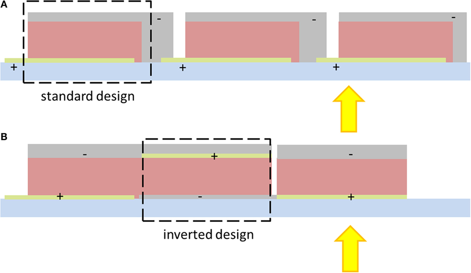
Figure 1. (A) Monolithic module interconnection and (B) alternative module design.
Individual cells are connected by extending the top/bottom electrode layer to the neighboring solar cell. This design has favorable electrical properties and the spacing between solar cells, i.e., the inactive module area can be very small. The standard device stack is often made of the following layers: a transparent electrode layer over-coated with PEDOT:PSS (poly(3,4-ethylenedioxythiophene):poly(styrenesulfonate)), followed by the photoactive layer and a metal electrode with a low work function. The inverted device comprises a transparent electrode, an interlayer which forms an electron-selective contact to the photoactive layer [e.g., zinc oxide (ZnO) or titanium oxide (TiOx)] (Waldauf et al., 2006) or converts the transparent electrode into electron-selective contact (e.g., polyethyleneimine) (Zhou et al., 2012; Udum et al., 2014). On top of the interlayer, the photoactive layer is deposited followed by a hole-selective interlayer [PEDOT:PSS or molybdenum oxide (MoOx)] and a metal electrode.
The inverted device design offers many advantages including improved device stability when exposed to ambient conditions. In the standard design, often a low work-function metal is required as top electrode (e.g., calcium or aluminum) which oxidizes quickly in the presence of oxygen and/or water. By contrast, high work-function metals such as silver or gold can be used for the hole-selective metal top electrode in inverted solar cells. Fully printed inverted devices have been demonstrated which turned out to be very difficult for the standard device design (Krebs, 2008).
In this contribution, we summarize our work on different device designs which could be applied to realize simple interconnects between individual solar cells. We used PEDOT:PSS or MoOx as hole-selective interlayers, and polyethylenimine (PEI) to modify indium tin oxide (ITO) electrodes into electron-selective contacts. As absorber materials, we applied a blend of poly(3-hexylthiophene-2,5-diyl) (P3HT) and different fullerene derivatives. The overall goal was to realize a set of interconnected solar cells following the scheme illustrated in Figure 1B, which can be manufactured using printing and coating methods. All processes should be compatible with flexible polymeric substrates such as polyethylene terephthalate (PET). In the performed experiments, we use blade coating and spin coating for the deposition of the interlayers and the absorber layer. MoOx and metal electrodes were thermally deposited. This process may be compatible with roll-to-roll deposition or one may apply silver-pastes or nano-wire materials as the top-contact electrode layer. We also built organic light-emitting diodes applying the same device designs to demonstrate the versatility of applied layer stacks and to learn more about the limitations of the investigated interfacial layers.
Experimental Section
Regio-regular poly(3-hexylthiophene-2,5-diyl) (P3HT, Rieke Metals), [6,6]-phenyl-C61-butyric acid methyl ester (PCBM), bis(1-[3-(methoxycarbonyl)propyl]-1-phenyl)-[6,6]C62 (bis-PCBM) (Solenne BV), PEI (branched, Mw = 800 g mol−1, Sigma Aldrich), poly(3,4-ethylenedioxythiophene):poly(styrenesulfonate) (PEDOT:PSS, Clevios PH 1000, and PVP Al 4083, Heraeus), Zonyl® FS-300 fluorosurfactant (40% in H2O, Fluka), dimethyl sulfoxide (DMSO, Anal R, VWR chemicals), and poly(2-methoxy-5-(2-ethylhexyloxy)-1,4-phenylene-vinylene) (MEH-PPV) end capped with polysilsesquioxane (POSS)-coded ADS200RE (Mw = 100,000 g mol−1, American Dye Source Inc.) were used as received without further purification. The chemical structures of the used organic semiconductors and interlayer materials are shown in Figure 2. All manipulations for the fabrication of devices were performed in ambient atmosphere if not stated otherwise. For the fabrication of either standard or inverted BHJ, solutions of P3HT:PCBM and P3HT:bis-PCBM (1:0.8 and 1:1 weight ratio, respectively) were prepared in chlorobenzene (40 mg ml−1). For OLEDs, the orange-emitting polymer ADS200RE was dissolved in chlorobenzene (8 mg ml−1). Pre-patterned glass/ITO and bare glass substrates were cleaned by ultrasonication in acetone, isopropanol, Helmanex® detergent, and deionized water successively. Flexible ITO-coated PET substrates were cleaned using, isopropanol, Helmanex® detergent, and deionized water successively. PEDOT:PSS (Clevios PH1000, 5% DMSO, 0.7 vol% Zonyl) was spin coated at 1000 rpm for 60 s, patterned and annealed at 140°C for 10 min, then rinsed with isopropanol to remove the excess Zonyl, and then annealed for another 10 min at 140°C. For all inverted devices, PEI in n-butanol (0.27 mg ml−1) was spin coated on top of cleaned and O2-plasma-treated glass/ITO, PET/ITO, and PEDOT:PSS (Clevios PH 1000, 5% DMSO, 0.7 vol% Zonyl)-coated glass substrate at 3000 rpm and then annealed on a hot plate (105°C for 10 min). After cooling down, P3HT:PCBM or P3HT:bis-PCBM solution for OPVs and ADS200RE solution for OLEDs was spin coated on top of PEI. A layer of PEDOT:PSS (Clevios PVP Al 4083, 0.7 vol% Zonyl) was spin coated on top of the active layer and then annealed at 110°C for 20 min inside a glove box (dry N2 atmosphere), or MoOx (10 nm) was deposited via thermal evaporation before the devices were finalized by the deposition of a silver electrode (ca. 100 nm).
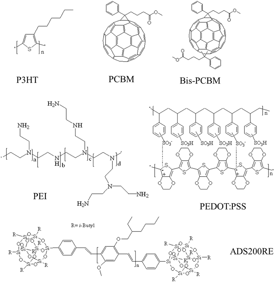
Figure 2. Photoactive and interlayer materials.
For the standard device, low conductivity PEDOT:PSS PVP Al 4083 was spin coated onto the cleaned ITO followed by the deposition of the active layer. In the next step, samples were transferred into a glove box and annealed for 10 min at 120°C (OPVs) and 90°C (OLEDs). Standard OPVs and OLEDs were completed by vacuum evaporation (~3 × 10⁻⁶ bar) of the top contact [0.8 nm LiF and 100 nm aluminum (OPVs), or 20 nm of calcium and 100 nm of silver (OLEDs)].
For blade-coated devices, pre-patterned glass/ITO substrates were cleaned, as described earlier. For the inverted solar cells, PEI (0.27 mg ml−1 dissolved in butanol) was coated on a heated substrate (70°C, blade speed of 5 mm s−1). The PEI-film was dried at 105°C on a hot plate for 10 min before the deposition of the photoactive layer. For standard devices, PEDOT:PSS (PVP Al 4083) diluted with water (1:2 volume ratio) was coated on a heated substrate (70°C, blade speed of 5 mm s−1). The absorber layer solution [P3HT (12 mg ml−1) and PCBM (8 mg ml−1) dissolved in chlorobenzene] was blade coated on a heated substrate coated with PEI or PEDOT:PSS (75°C, blade speed of 15 mm s−1). Inverted devices were finalized with the deposition of MoOx (10 nm) and silver (100 nm). For another standard devices layout, a thin layer of a PEI:PCBM blend [1 mg ml−1 PCBM, 0.8 mg ml−1 PEI dissolved in a butanol/anisole solution (19:1 volume ratio)] was coated on top of the photoactive layer at a temperature of 80°C and a blade speed of 10 mm s−1. These standard devices were finalized with a silver electrode (100 nm) deposited by thermal evaporation.
Current density–voltage (J–V) characteristics were measured under AM 1.5 white light illumination (100 mW cm−2 solar simulator) using a Keithley 2400 Source-Meter-Unit. External quantum efficiency (EQE) measurements were conducted using 90 W Xenon lamp as light source connected via an optical fiber to an ACTON Spectra Pro150 monochromator and an EG&G 7260 DSP Lock-in amplifier. The performance of the fabricated OLEDs was measured using an Agilent B1500 parameter analyzer with two source meter units, one driving the OLED and one measuring the resulting photocurrent of a silicon photodiode. The electroluminescence (EL) spectra of OLEDs were recorded using a Photo Research Spectra scan PR-655 CCD camera and by applying constant current density with Keithley SMU 2401.
Results and Discussion
Figure 3 shows all the device stacks prepared in this study. Figure 3E illustrates the realized alternative interconnection of two solar cells with alternating polarities. The performance of the different solar cells is discussed below in detail. In addition, we built light-emitting diodes based on the layer stacks (Figures 3A–D). Although we found that the performance of all inverted OLEDs is significantly reduced compared with the reference device, it is interesting to see that all tested configurations allow the preparation of working devices. The luminance–current density–voltage (L–J–V) curves are also shown below for the different device designs.
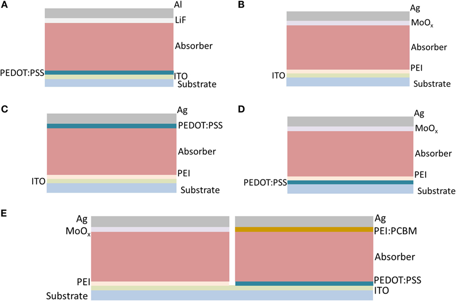
Figure 3. (A) Standard device (reference), (B) inverted device with MoOx as hole-selective interlayer, (C) inverted device with PEDOT:PSS as hole-selective interlayer, (D) inverted device with PEDOT:PSS as electron-selective interlayer, (E) inverted and standard device connected through the ITO electrode.
ITO as an Electron-Selective Electrode and MoOx as a Hole-Selective Layer
Figure 4A shows the J–V curves of standard OPV devices with the layer stack glass/ITO/PEDOT:PSS/P3HT:PCBM or bis-PCBM/LiF/Al (Figure 3A). In Figure 4B, the J–V curves of inverted devices (Figure 3B) with the structure glass/ITO/PEI/P3HT:PCBM or bis-PCBM/MoOx/Ag are plotted. The inverted and standard devices showed comparable diode dark currents, short circuit currents, and fill factors. For inverted devices, slightly higher open-circuit voltages and electrical fill factors (FF) were found yielding about 10% higher power conversion efficiencies. It is interesting to note that the ITO/PEI electrode can form excellent contacts to fullerene derivatives with different electron affinities (Lenes et al., 2008).
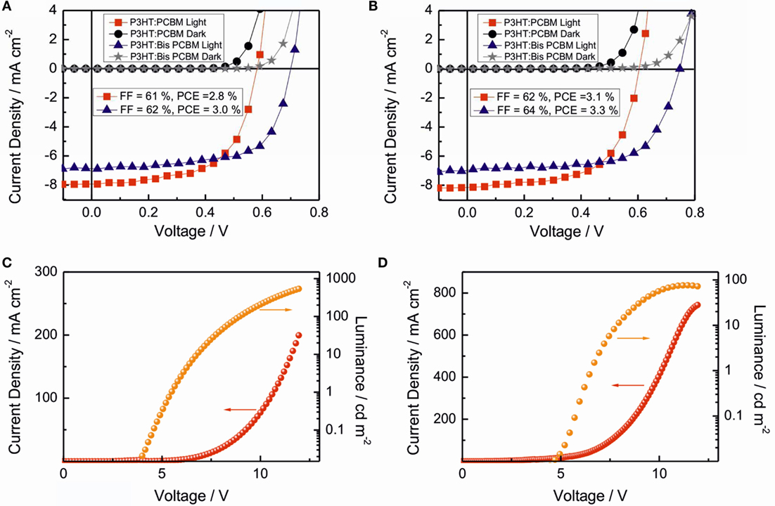
Figure 4. J–V and L–J–V characteristics of standard and inverted BHJ OPVs and OLEDs: (A) glass/ITO/PEDOT:PSS/P3HT:PCBM or bis-PCBM/LiF/Al, (B) glass/ITO/PEI/P3HT:PCBM or bis-PCBM/MoOx/Ag, (C) glass/ITO/PEDOT:PSS/ADS200RE/Ca/Ag, and (D) glass/ITO/PEI/ADS200RE/MoOx/Ag configurations, respectively.
The L–J–V characteristics of ADS200RE-based OLEDs prepared in the standard and inverted configuration are illustrated in Figures 4C,D. Both devices exhibit similar onset and operating voltages. However, a lower luminance of ~58 cd m−2 at 10 V and a maximum luminance of ~80 cd m−2 were found in the inverted OLEDs, while the standard OLEDs showed 208 cd m−2 at 10 V and highest luminance of ~847 cd m−2. These findings illustrate that the PEI/MoOx interlayers are not ideal for the selected polymer emitter. Despite the high injection currents found for the inverted device, the luminance is about one order of magnitude lower. This might be an indication for an unbalanced charge carrier (electrons and holes) injection into the emitter layer caused by different injection barriers formed at the interlayer–semiconductor interface. The work function of the ITO-PEI stack was found to be in the range of 3.5 eV, whereas the LUMO position of the emitter polymer is ~3 eV (Zhou et al., 2012). This large offset may be the origin of the reduced luminance of the studied inverted OLEDs.
As expected, the stability of inverted OLEDs was found to be much better compared with the standard devices with low work-function metal electrode, when operated under ambient conditions. While standard devices showed a gradual reduction of the EL and showed no emission after about 90 min of continuous operation in air, the OLEDs with the air-stable top electrodes could be operated for several hours without a significant reduction of the EL intensity.
PEDOT:PSS as a Hole-Selective Layer and ITO as an Electron-Selective Electrode
By replacing the inorganic hole-selective layer MoOx by PEDOT:PSS, efficient BHJ OPVs and OLEDs can be prepared (Figure 3C). In Figure 5A, the inverted BHJ with the layer sequence glass/ITO/PEI/P3HT:PCBM or bis-PCBM/PEDOT:PSS/Ag showed photovoltaic performances comparable to solar cells with a MoOx interlayer and the reference devices (Figures 4A,B). The same device stack was also built on a flexible substrate and comparable efficiencies were found for rigid and flexible solar cells (Figures 5A,B). These results suggest that the vacuum-deposited MoOx layer can be replaced by a solution-processed PEDOT:PSS without significant performance losses in inverted BHJ solar cells.
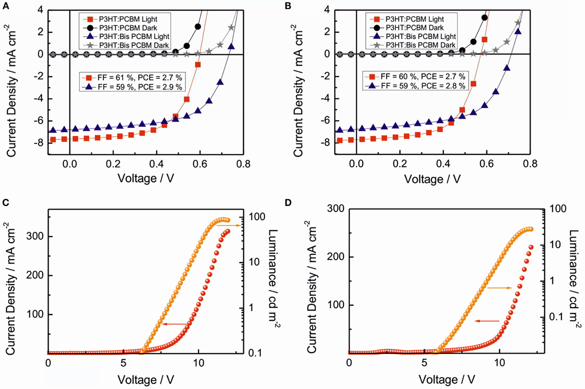
Figure 5. J–V characteristics of the OPVs: (A) glass/ITO/PEI/P3HT:PCBM or bis-PCBM/PEDOT:PSS/Ag, (B) PET/ITO/PEI/P3HT:PCBM or bis-PCBM/PEDOT:PSS/Ag and L–J–V characteristics of OLEDs: (C) glass/ITO/PEI/ADS200RE/PEDOT:PSS/Ag, and (D) PET/ITO/PEI/ADS200RE/PEDOT:PSS/Ag.
Figures 5C,D show the characteristics of OLEDs with the layer sequence glass/ITO/PEI/ADS200RE/PEDOT:PSS/Ag and PET/ITO/PEI/ADS200RE/PEDOT:PSS/Ag, respectively. Devices exhibited a luminance of ~100 cd m−2 on glass (Figure 5C) and ~30 cd m−2 on PET (Figure 5D) which is comparable to the OLEDs fabricated with a MoOx layer (Figure 4D). The presented results indicate the investigated MoOx/Ag and PEDOT:PSS/Ag electrodes exhibit similar charge extraction and injection efficiencies.
Figure 6A shows the EQE spectra of flexible solar cells with PET/ITO/PEI/P3HT:PCBM or bis-PCBM/PEDOT:PSS/Ag with its maximum at 525 nm. Figure 6B shows the photograph of the corresponding flexible solar cell. In Figure 6C, the normalized extinction and spectrum of the OLED with PET/ITO/PEI/ADS200RE/PEDOT:PSS/Ag is displayed. Photographs of the corresponding flexible OLED are shown in Figure 6D. The presented results demonstrate that the explored device architectures can easily be transferred to flexible substrates.
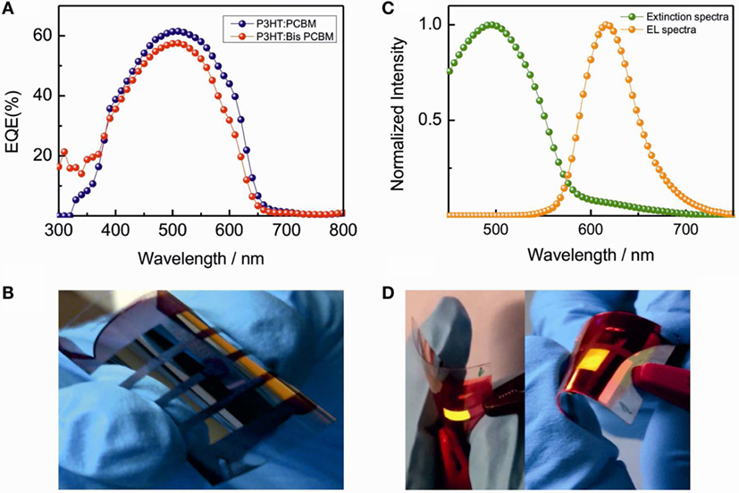
Figure 6. (A,B) EQE spectra of the solar cells with PET/ITO/PEI/P3HT:PCBM or bis-PCBM/PEDOT:PSS/Ag, and the photograph of the corresponding flexible solar cell, respectively, and (C) normalized extinction and electroluminescence spectra of the OLEDs with PET/ITO/PEI/ADS200RE/PEDOT:PSS/Ag, and (D) the photograph of the corresponding flexible OLED while operated in air.
Highly Conductive PEDOT:PSS as an Electron-Selective Electrode and MoOx or PEDOT:PSS as a Hole-Selective Layer
The second type of inverted design realized in this work is based on a high conductivity PEDOT:PSS/PEI stack used as an electron-selective electrode and MoOx (Figure 3D) or PEDOT:PSS (Clevios PVP Al 4083) as hole selective contact. In this structure, ITO is replaced by PEDOT:PSS. A silver bus bar deposited between the substrate and the PEDOT:PSS layer can be used to support the conductivity of the semitransparent electrode. Applying PEDOT:PSS electrodes on both sides of the photoactive layer leads to a semitransparent device and a fully solution processed device stack. As shown in Figure 7A, with glass/PEDOT:PSS/PEI/P3HT:PCBM or bis-PCBM/MoO3/Ag stacks, reasonable solar cell performances could be achieved with good fill factor (>60%). The smaller short circuit current density compared with the ITO-based devices might be caused by additional optical losses in the PEDOT:PSS layer.
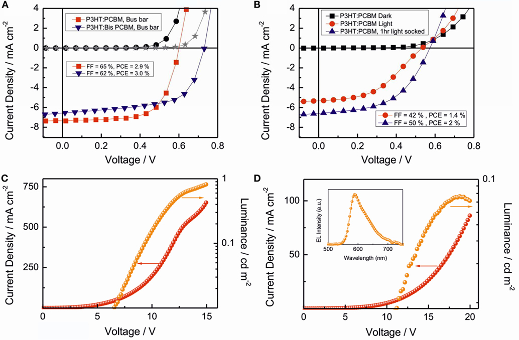
Figure 7. J–V characteristics of the OPVs: (A) glass/PEDOT:PSS/PEI/P3HT:PCBM or bis-PCBM/MoOx/Ag, and (B) glass/PEDOT:PSS/PEI/P3HT:PCBM/PEDOT:PSS/Ag; L–J–V characteristics of OLEDs: (C) glass/PEDOT:PSS/PEI/ADS200RE/MoOx/Ag, and (D) glass/PEDOT:PSS/PEI/ADS200RE/PEDOT:PSS/Ag. The inset in (D) displays the EL spectrum of corresponding OLEDs.
Figure 7B shows the results obtained when using low conductivity PEDOT:PSS (Clevios PVP Al 4083) instead of MoOx. The freshly prepared device showed losses in all electrical parameters but after light soaking for 1 h, a significant improvement in all the electrical parameters was observed. This suggests that defects or traps states are present in the as-prepared devices. Residual water which is trapped in the PEDOT:PSS layers and forming interface dipoles may be responsible for the S-shaped J–V curve observed for fresh devices. Upon long-term illumination, dipoles re-arrange and the expected J–V curve can be measured. The S-shaped J–V curve recovered when the device is stored in the dark overnight.
Prepared OLEDs exhibited, despite reasonable current densities, a much lower luminance compared to the standard OLEDs (Figure 4C). The device based on a MoOx/Ag top electrode showed a luminance of ~1 cd m−2 at 15 V (Figure 7C) while for the OLED with two PEDOT:PSS electrodes only 0.1 cd m−2 were found at very high operating voltages (Figure 7D). The relatively high onset voltage and the weak EL found in both devices suggests that the PEDOT:PSS/PEI electrode is not ideal for the injection of electrons into the emitter layer. Also unbalanced electron and hole injection and the presence of interface dipoles or traps, causing the S-shaped J–V characteristics in the corresponding solar cells, may limit the performance of the investigated OLEDs. By contrast, in solar cells, the extraction of photo-generated electrons through the PEDOT:PSS/PEI is working well. This suggests that a selective contact is formed between the tested fullerene acceptors and the cathode.
PEDOT:PSS as a Hole-Selective and PCBM:PEI as an Electron-Selective Layer
The last layer stack we tested was a standard device with high work-function top electrode (Figure 3E). In the first set of experiments, we deposited thin layers of PEI on top of the absorber layer and finished the device with a vacuum-deposited silver electrode. This approach did not result in working solar cells. Either we found non-selective contacts and the solar cells showed very small open-circuit voltages and poor diode characteristics or the contact was blocking any electrical current flow through the device. The non-selective contacts may be caused by too thin or inhomogenous PEI layers, while in the case of blocking contacts the layers were too thick. To overcome this problem, we added small amounts of PCBM to the PEI solution. With this we tried to mimic the approach by Page et al. (2014). By introducing a thin layer of a fullerene derivative with amine substitutions as an interlayer between the absorber layer and the metal electrode, the authors built highly efficient solar cells using a high work-function metal such as Au, Ag, or Cu as top electrode. In our experiments, the PEI:PCBM blend should play the role of the amine-substituted fullerene derivative. With this approach, we were able to build working solar cells with reasonable performance. However, the deposition of the PEI:PCBM layer by blade- or spin-coating was found to be very tricky. The different solubility characteristics of the two components, PEI and PCBM, required the usage of a solvent mixture, butanol and anisol. The resulting solution, however, interacted with the photoactive layer during the deposition process resulting in inhomogeneities and defects in the layer stack. All this leads to a low device preparation yield, and clearly more work is required to establish a stable and reproducible manufacturing process. Applying amine-substituted fullerene derivatives or fullerenes compatible with PEI solvents appear to be the most promising strategies to overcome the current limitations. The current–voltage curve of a solar cell prepared after some optimization of the PEI:PCBM formulation is shown in Figure 8A. The devices still suffers from a reduced open-circuit voltage, electrical fill factor, and photocurrent compared with typical P3HT/PCBM devices.
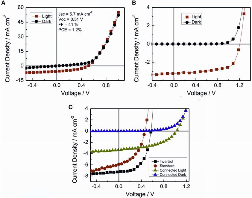
Figure 8. J–V curves of (A) a standard device with a PEI:PCBM electron-selective interlayer and silver top contact, (B) a standard (glass/ITO/PEDOT:PSS/P3HT:PCBM/LiF/Al) and an inverted (glass/ITO/PEI/P3HT:PCBM/MoOx/Ag) device connected in series by a common ITO electrode, (C) a standard device with a PEI:PCBM electron-selective interlayer and silver top electrode, and an inverted (glass/ITO/PEI/P3HT:PCBM/MoOx/Ag) device connected in series with a common ITO electrode measured combined and independently.
In the next step, we used this device architecture to build small modules based on standard and inverted solar cells processed on the same substrate.
Interconnected Standard and Inverted Solar Cells
The different device designs discussed earlier were used to test the interconnect scheme suggested in Figure 1B. Using blade-coating for the deposition of the organic layers, a standard and an inverted cell stack were fabricated on an ITO-coated substrate. In the first configuration, the standard and the inverted solar cells were based on the layer stacks glass/ITO/PEDOT:PSS/Absorber/LiF/Al and glass/ITO/PEI/Absorber/MoOx/Ag, respectively. The ITO contact was acting as interconnect between the two devices. The resulting J–V curves measured with and without illumination are shown in Figure 8B. As the devices were connected in series, the voltages delivered by the two solar cells add up yielding an open-circuit voltage of ~1.2 V. Excellent electrical fill factors in the range of 65% were observed for the interconnected inverted and standard solar cells. As the active device area is doubled, the short circuit current density is reduced by a factor of 2. The only drawback of this configuration is that the top electrode of the standard device degrades quickly under ambient conditions and cannot be solution processed.
Figure 8C shows the individual J–V curves of a standard and an inverted solar cell processed on the same ITO-coated substrate with the structures glass/ITO/PEDOT:PSS/Absorber/PEI:PCBM/Ag and glass/ITO/PEI/Absorber/MoOx/Ag recorded under illumination and the resulting J–V characteristics when the two devices are connected via the ITO electrode. We measured an open-circuit voltage of 0.57 V, a fill factor of 0.55, and a short circuit current density of 7.4 mA cm−2 for the inverted device. For the standard device with the PEI:PCBM interlayer, a Voc of 0.46 V, a FF of 0.46, and a short circuit current density of 5.9 mA cm−2 were found.
For the interconnected devices, the voltages add up resulting in an open-circuit voltage of 1.03 V but due to the moderate performance of the involved standard device the overall performance is rather low with a FF of 0.47 and a short circuit current density of 3.33 mA cm−2 (Figure 8C). The two examples illustrate that the presented device designs allow the realization of the improved interconnection scheme proposed in Figure 1. Upon further optimization of the electron-selective (PEI:PCBM), a very simple procedure to build organic photovoltaic modules on a transparent electrode with a small number of components (PEDOT:PSS, PEI, absorber blend, and vacuum-deposited silver) appears to be feasible. The vacuum-deposited silver may also be replaced by a printed silver layer, leading to a fully printable organic photovoltaic module with improved electrical interconnects.
Summary
We have explored organic bulk-heterojunctions solar cells and light-emitting diodes in the so-called standard and inverted configuration testing different interlayer materials. Obtained device parameters are summarized in Table 1.
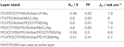
Table 1. Device parameter obtained for the indicated layer stack.
While all tested interlayer combinations allowed the preparation of BHJ with reasonable performance, only a combination of ITO/PEI and MoOx/Ag interlayers resulted in OLEDs with a performance comparable to the reference device. We speculate that a reduced charge injection efficiency is limiting the luminance of the other OLEDs prepared in the study. Based on the tested layer stacks, we demonstrated modules of two solar cells with alternating electrode polarity on a common electrode forming the interconnect. The proposed device architectures and the module design can be manufactured by printing and coating methods and could be a highly relevant alternative to the monolithic interconnect scheme used today.
Author Contributions
GA, BM, CU, and PD prepared and characterized the solar cells and light-emitting diodes described in the manuscript. CH and MS supervised the research. All authors contributed to the manuscript preparation.
Conflict of Interest Statement
The authors declare that the research was conducted in the absence of any commercial or financial relationships that could be construed as a potential conflict of interest.
Funding
GA and MS would like to acknowledge the Austrian Research Promotion Agency (FFG) (flex!PV 838621, flex!PV_2.0 853603) for financial support. BM acknowledges financial support by the Erasmus Mundus Mobility Project GATE.
References
Etxebarria, I., Ajuria, J., and Pacios, R. (2015). Solution-processable polymeric solar cells: a review on materials, strategies and cell architectures to overcome 10%. Org. Electron. 19, 34–60. doi:10.1016/j.orgel.2015.01.014
Gaudian, R. (2010). “Photovoltaic Module,” World Intellectual Property Organization, Patent Application WO2010083161 (A1).
Krebs, F. C. (2008). Air stable polymer photovoltaics based on a process free from vacuum steps and fullerenes. Sol. Energy Mater. Sol. Cells 92, 715–726. doi:10.1016/j.solmat.2008.01.013
Lee, J., Back, H., Kong, J., Kang, H., Song, S., Suh, H., et al. (2013). Seamless polymer solar cell module architecture built upon self-aligned alternating interfacial layers. Energy Environ. Sci. 6, 1152. doi:10.1039/c3ee24454g
Lee, J., Back, H., Kong, J., Park, D.-W., and Lee, K. (2012). New series connection method for bulk-heterojunction polymer solar cell modules. Sol. Energy Mater. Sol. Cells 98, 208–211. doi:10.1016/j.solmat.2011.11.008
Lenes, M., Wetzelaer, G. A. H., Kooistra, F. B., Veenstra, S. C., Hummelen, J. C., and Blom, P. W. M. (2008). Fullerene bisadducts for enhanced open-circuit voltages and efficiencies in polymer solar cells. Adv. Mater. 20, 2116–2119. doi:10.1002/adma.200702438
Machui, F., Hösel, M., Li, N., Spyropoulos, G. D., Ameri, T., Søndergaard, R. R., et al. (2014). Cost analysis of roll-to-roll fabricated ITO free single and tandem organic solar modules based on data from manufacture. Energy Environ. Sci. 7, 2792. doi:10.1039/C4EE01222D
Page, Z. A., Liu, Y., Duzhko, V. V., Thomas, P., Emrick, T., Russell, T. P., et al. (2014). Fulleropyrrolidine interlayers: tailoring electrodes to raise organic solar cell efficiency. Science 346, 441. doi:10.1126/science.1255826
Scharber, M. C. (2016). On the efficiency limit of conjugated polymer:fullerene-based bulk heterojunction solar cells. Adv. Mater. 28, 1994–2001. doi:10.1002/adma.201504914
Udum, Y., Denk, P., Adam, G., Apaydin, D. H., Nevosad, A., Teichert, C., et al. (2014). Inverted bulk-heterojunction solar cell with cross-linked hole-blocking layer. Org. Electron. 15, 997–1001. doi:10.1016/j.orgel.2014.02.009
Waldauf, C., Morana, M., Denk, P., Schilinsky, P., Coakley, K., Choulis, S. A., et al. (2006). Highly efficient inverted organic photovoltaics using solution based titanium oxide as electron selective contact. Appl. Phys. Lett. 89, 233517. doi:10.1063/1.2402890
Xu, T., and Yu, L. (2014). How to design low bandgap polymers for highly efficient organic solar cells. Mater. Today 17, 11–15. doi:10.1016/j.mattod.2013.12.005
Zhao, J., Li, Y., Yang, G., Jiang, K., Lin, H., Ade, H., et al. (2016). Efficient organic solar cells processed from hydrocarbon solvents. Nat. Energy 1, 15027. doi:10.1038/nenergy.2015.27
Keywords: bulk-heterojunction solar cell, interlayer, module design, photovoltaics, solar energy
Citation: Adam G, Munkhbat B, Denk P, Ulbricht C, Hrelescu C and Scharber MC (2016) Different Device Architectures for Bulk-Heterojunction Solar Cells. Front. Mater. 3:39. doi: 10.3389/fmats.2016.00039
Received: 12 April 2016; Accepted: 29 July 2016;
Published: 23 August 2016
Edited by:
Theodoros Dimopoulos, Austrian Institute of Technology, AustriaReviewed by:
Josep Albero, Institute of Chemical Technology (CSIC-UPV), SpainIoanna Giouroudi, Vienna University of Technology, Austria
Copyright: © 2016 Adam, Munkhbat, Denk, Ulbricht, Hrelescu and Scharber. This is an open-access article distributed under the terms of the Creative Commons Attribution License (CC BY). The use, distribution or reproduction in other forums is permitted, provided the original author(s) or licensor are credited and that the original publication in this journal is cited, in accordance with accepted academic practice. No use, distribution or reproduction is permitted which does not comply with these terms.
*Correspondence: Markus C. Scharber, markus_clark.scharber@jku.at