Low-Loss Slot Waveguides with Silicon (111) Surfaces Realized Using Anisotropic Wet Etching
 Kapil Debnath1*
 Ali Z. Khokhar2
 Stuart A. Boden1
 Hideo Arimoto1
 Swe Zin Oo1
 Harold M. H. Chong1
 Graham T. Reed2
  Shinichi Saito1
- 1Faculty of Physical Sciences and Engineering, University of Southampton, Southampton, UK
- 2Optoelectronics Research Centre, University of Southampton, Southampton, UK
We demonstrate low-loss slot waveguides on silicon-on-insulator platform. Waveguides oriented along the (11-2) direction on the Si (110) plane were first fabricated by a standard e-beam lithography and dry etching process. A tetramethylammonium hydroxide-based anisotropic wet etching technique was then used to remove any residual side wall roughness. Using this fabrication technique, propagation loss as low as 3.7 dB/cm was realized in silicon slot waveguide for wavelengths near 1550 nm. We also realized low propagation loss of 1 dB/cm for silicon strip waveguides.
Introduction
The slot waveguide structure was first proposed by Almeida et al. (2004) as a simple way to achieve extremely strong optical confinement in a low refractive index medium. Typically, an all-dielectric slot waveguide is formed by two high index waveguiding regions (e.g., silicon) separated by a narrow region of low index material (e.g., air, silica or polymer). Due to the discontinuity in the electric field at the high index contrast interfaces, such a structure supports an optical mode which can confine and guide light along the nanometer-size region of low index material, as shown in Figure 1. This unique property of slot waveguides has been exploited in many areas such as sensing (Barrios et al., 2007; Carlborg et al., 2010), non-linear optics (Muellner et al., 2009; Martínez et al., 2010), electro-optic modulation (Baehr-Jones et al., 2008; Chen et al., 2009; Koos et al., 2009), light sources (Guo et al., 2012; Tengattini et al., 2013), etc. However, a major limitation of slot waveguides is their high propagation loss. Since the light is more confined in the slot region, any surface roughness, introduced during the fabrication process, causes significant scattering loss. Therefore, fabrication of low-loss slot waveguides is challenging and the lowest reported propagation loss was 10 dB/cm (Baehr-Jones et al., 2005), from a standard vertical slot waveguide. There are different approaches proposed in the literature to reduce this propagation loss. For example, strip-loaded slot waveguides have been proposed with improved propagation loss of 6.5 dB/cm (Ding et al., 2010); albeit for a reduced mode confinement in the slot region. Spott et al. (2011) reported a record low propagation loss of 1.7 dB/cm from a slot waveguide by introducing different silicon arm widths. This geometry also compromises the mode confinement in the slot region due the asymmetry in the waveguide geometry. Alasaarela et al. (2011) adopted a different approach to reduce the propagation loss by coating the waveguide surface by a thin layer of titanium dioxide. This layer with intermediate refractive index effectively reduces the optical field intensity at the high index contrast interface, and they reported a propagation loss of 7 dB/cm for a slot waveguide.
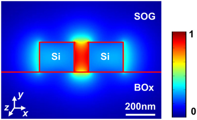
Figure 1. Dominant electric field (│Ex│) of the fundamental TE mode guided by the silicon slot waveguide on a buried oxide (BOx) substrate with a spin-on glass (SOG) surrounding medium. The waveguide is 220 nm high, and the slot width is 100 nm with 225 nm wide silicon arms on both sides.
In this letter, we present a new and simple method of reducing waveguide loss by surface smoothening using a combination of dry and anisotropic wet etching processes. The wet etching process was used to smoothen the residual side wall roughness after dry etching. Here, we used an aqueous solution of tetramethylammonium hydroxide (TMAH), which is widely used for anisotropic wet etching of silicon. Due to its strong alkalinity, TMAH reacts very differently with silicon depending on the crystallographic orientation of the exposed region. For example, while (100) and (110) planes are etched by a TMAH solution, (111) plane remains almost unaffected. Since this is a completely chemical process and strongly depends on the crystallographic orientation of the etched surface, ideally we should expect an ultra-smooth surface with atomic level irregularity. Previously sub-dB propagation loss in silicon strip waveguides has been demonstrated using TMAH-based wet etching process (Lee et al., 2001; Debnath et al., 2016). In this work, by combining dry and wet etching processes, we managed to reduce the propagation loss of a slot waveguide with 200-nm slot width from 10.5 to 3.7 dB/cm and for a strip waveguide from 2.7 to 1 dB/cm.
Fabrication Process
The fabrication process flow is shown in Figure 2. The slot waveguides were fabricated on two silicon-on-insulator (SOI) substrates, namely sample A and sample B. Both the SOI substrates had 220 nm thick layers of Si with (110) surface orientation on 2 μm thick buried oxide (BOx). The advantage of choosing the (110)-oriented substrate lies in the fact that (111) planes are normal to the (110) surface along (112) direction. As a result, when the waveguides are designed along the (112) directions, the (111) planes will act as an etch stop during the smoothening process. During the fabrication process, first a 20-nm thick layer of SiO2 was thermally grown by annealing the SOI substrates at 1000°C in O2 (dry anneal) for 6 min in a quartz furnace tube. The substrates were then spin coated with a 250-nm thick ZEP-520A positive e-beam resist layer. Using e-beam lithography, the desired waveguide patterns were exposed onto the ZEP layer via a 5-nm spot size. The waveguides were designed to align along the (11-2) direction on the SOI substrates. After developing the exposed resist layer, the waveguide patterns were transferred to the SiO2 hard mask and subsequently to the SOI layer in an inductively coupled plasma (ICP) etcher using a SF6/C4F8 chemistry. After the dry etching process, the remaining resist was removed in an O2 plasma asher. Final cleaning was carried out in fuming nitric acid and then diluted hydrofluoric acid. Surface roughness smoothening using anisotropic wet etching was carried out only on sample B. To avoid the formation of any native oxide layer, immediately after the HF cleaning process, the substrate was immersed in a 25% aqueous solution of TMAH at room temperature for 10 min. This duration was sufficient to significantly reduce the roughness from the waveguide surfaces. During this wet etching process, the top surfaces of the waveguides were protected by the SiO2 hard mask while any roughness on the waveguide side walls was reduced. Since the etch rate is very slow along the (111) direction, we expect an atomically flat and vertical side walls after the wet etching process. For comparison, the wet-etching step was omitted for sample A. Figures 3A,B show the SEM images of the slot waveguides without (sample A) and with (sample B) roughness smoothening using TMAH wet etching, respectively. From the images, it is obvious that the surface roughness has been significantly reduced after the wet etching process. We have further carried out a detailed sidewall roughness analysis using atomic force microscopy (AFM). We have used a special tapered AFM tip from Bruker (CDF100) to easily access the vertical side walls of the waveguides. The AFM image was then processed using Gwyddion AFM analysis software to extract the surface roughness information of the sidewalls. In the Figures 3C,D, the y-axis is along the length and the x-axis is along the height of the waveguide, whereas the surface roughness is represented along z-axis. The AFM images clearly reveals that the roughness reduces from an rms value of 6.7 nm (Figure 3C) for the dry etched waveguide to 1.4 nm (Figure 3D) for the wet etched waveguide. It is also important to note here that the slot waveguides which had undergone the wet etching step had 20 nm larger slot width than designed, due to the slow etching of (111) plane. This slow etching of the (111) plane can also be used to precisely control the slot width by simply optimizing the wet etching time. Although, in this work, we have used e-beam lithography due to its quick turned around time, the same wet etching process can be used to smoothen the waveguide surfaces realized using standard photolithography processes. Finally, another thermal oxidation was carried on both the substrates to grow a 5-nm thick layer of SiO2, which acts as a surface passivation layer. In most applications, the slot waveguides are cladded with low index materials, such as polymers (Koos et al., 2009) or silica (Martínez et al., 2010). Here, we spin coated the substrate with 500-nm thick spin-on glass (SOG; Fox-16, Dow Corning) and annealed at 400°C in N2 environment for 4 h to cure the SOG. This acts as a low-loss cladding for the slot waveguides which has the refractive index of around 1.45, similar to silica.
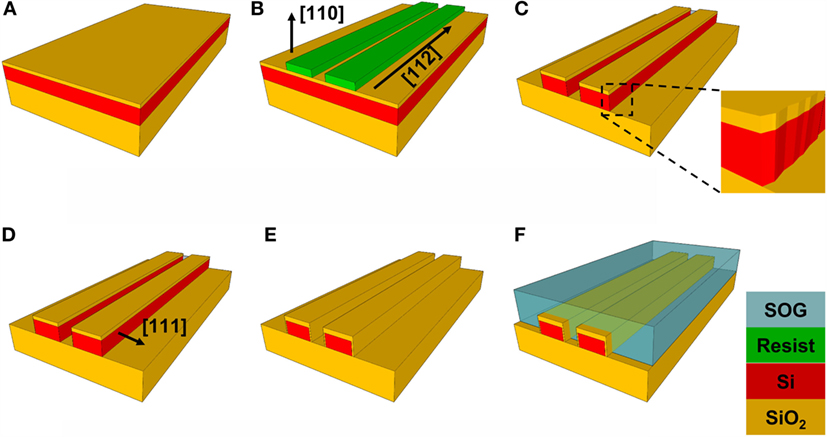
Figure 2. Fabrication process flow: (A) a 20-nm thick layer of SiO2 was thermally grown on SOI substrate; (B) slot and strip waveguide patterns were written on the resist layer using e-beam lithography; (C) waveguide patterns were transferred to the silicon layer using ICP dry etching process; (D) SOI substrate was dipped into TMAH solution to remove any surface roughness (only for sample B); (E) a thin SiO2 layer was thermally grown to serve as surface passivation; and (F) finally, 500 nm thick layer of SOG was spin coated and cured.
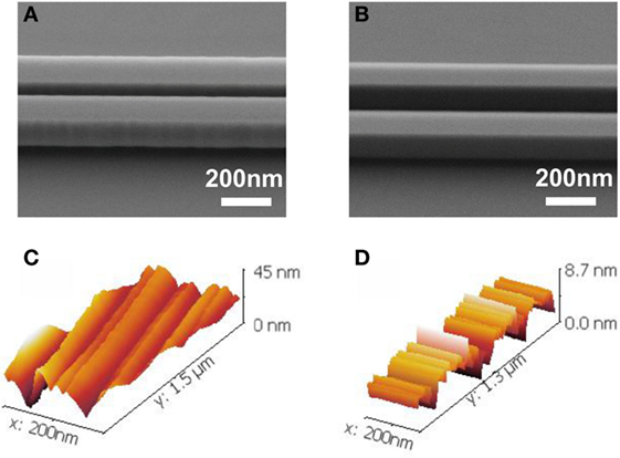
Figure 3. SEM images of a waveguide (A) on the dry etched only sample (sample A) and (B) on the TMAH-treated sample (sample B), imaged at an angle of 45°; (C) AFM image of the side wall of dry etched waveguide with rms roughness of 6.7 nm; (D) AFM image of the side wall of wet etched waveguide with rms roughness of 1.4 nm.
Measurement and Results
The transmission through the fabricated slot waveguides was measured using a fiber-coupled tunable laser source with a tuning range from 1530 to 1630 nm. For all the measurements, 10-dBm laser power was used. Since the slot mode is a TE mode, the input of only TE-polarized light was ensured with a fiber polarization controller. Coupling light onto the chip was achieved by fiber-grating couplers (Covey and Chen, 2013). The wavelength was scanned using the built-in sweeping ability of the laser, and the detector automatically recorded the output spectra. For both samples, the total fiber to fiber insertion loss was around 20 dB, which includes the system loss and the grating coupler losses. For estimating the propagation loss in the strip waveguide and slot waveguides, a cut-back method was used. Waveguides with four different lengths ranging from 2 to 8 mm were designed. For strip waveguides, the waveguide width was 450 nm. For slot waveguides, we designed three different slot widths of 100, 150, and 200 nm with 225-nm wide silicon arms on both sides. Figure 4 shows the normalized transmission spectra, represented in light colors, of a set of slot waveguides with fixed slot width of 100 nm and varied lengths. The peak transmission values for each length were estimated from the fitted curve using a quadratic function to match the grating coupler spectrum. The fitted curves are represented in dark colors in Figure 4. We also observed ~1 dB ripple in the measured transmission spectra. We attribute such fluctuations to the imperfect coupling region between the strip and slot section of the waveguide (shown in the inset of Figure 4). This is caused due to sudden change in effective index of the optical mode at the coupling region. The coupling efficiency between the strip and slot waveguide region can be improved by carefully designing the coupling region as proposed previously by Han et al. (2016), Säynätjoki et al. (2011), and Passaro and La Notte (2012).
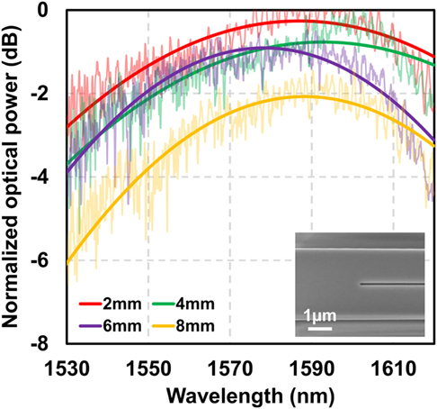
Figure 4. Spectrum and quadratic function fitting for different waveguide lengths with slot width of 100 nm. The inset shows the coupling region between the strip region and the slot region of the waveguide.
Figure 5 shows the cut-back measurement results for different waveguide geometries under different etching conditions. In order to avoid any unwanted variation in the coupling condition, for each propagation length, we have measured a set of four waveguides and considered the average value for estimating the propagation loss. To emphasize the effect of our surface smoothening process on the waveguide loss, we have also normalized the waveguide transmission by setting the background loss (i.e., setup and coupling loss) to 0 dB. In Figures 5A–D, the black circles represent the normalized transmission for dry etched waveguides on sample A and the red squares represent the normalized transmission of the waveguides after the surface smoothening step on sample B. The dashed lines represent the linear fits for the transmission data. For every waveguide geometry, we observed a significant reduction in the propagation loss. For strip waveguides the propagation loss reduced from 2.7 to 1 dB/cm, and for slot waveguides with 100, 150, and 220 nm the propagation loss dropped from 12 to 4.1, 10.7 to 5, and 10. 5 to 3.7 dB/cm, respectively. We expected the slot waveguide loss to monotonically reduce with increasing slot width, since the optical confinement also reduces with increasing slot width. However, we found that, although waveguide with 200 nm slot has lower loss in comparison to waveguide with 100 nm slot, the loss of 150 nm slot is relatively higher. We believe this is due to experimental error and within our error limit. Also, we would like to mention that 20 nm increase in slot width after wet etching should not have a significant effect on the propagation loss, and, according to our experimental results, for such variation in the slot width, we expect to see the loss value to change by less than 0.3 dB/cm.
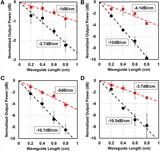
Figure 5. Normalized optical output power vs. waveguide length after dry etching (black circle) and wet etching (red square) for (A) strip waveguide with no slot and slot waveguides with slot widths of (B) 100 nm, (C) 150 nm, and (D) 200 nm.
Conclusion
To summarize, in this letter, we have proposed and demonstrated a simple fabrication technique to realize low-loss strip and slot waveguides on SOI platform. Here, we combined both dry and anisotropic wet etching processes to reduce propagation loss. The waveguides were first defined during the dry etching process and then the anisotropic wet etching process was used to remove any sidewall roughness. Using this fabrication technique, we realized a slot waveguide with a minimum propagation loss of 3.7 dB/cm for a slot width of 200 nm. There are several advantages of our proposed fabrication technique. First, without using any asymmetry or multilayer structures, the propagation loss can be reduced in a symmetric slot waveguide. Second, our surface smoothening technique can be applicable to patterns realized using standard photolithography. Finally the slow etching rate of the (111) plane can be used to precisely control the slot width.
Anisotropic wet etching is very selective to crystallographic orientation of silicon. Although, on the one hand, this allowed us to realize atomically flat surfaces and reduce propagation loss through silicon waveguides; due to its dependence on the crystallographic planes, our fabrication process restricts designing of nanophotonic components only along certain directions. This limitation can be avoided by adopting a hybrid fabrication process, where only certain components of the photonic integrated circuit, e.g., slot waveguide, undergoes the roughness smoothening process using anisotropic wet etching.
Data Availability
All data supporting this study are available upon request from the University of Southampton repository at http://dx.doi.org/10.5258/SOTON/397774.
Author Contributions
KD and SS conceived the idea. KD performed the device design and simulation. KD and AK performed the fabrication. SB performed the SEM imaging. SO performed the AFM imaging. KD wrote the manuscript. All the authors were involved in the analysis of the results and revision of the manuscript.
Conflict of Interest Statement
The authors declare that the research was conducted in the absence of any commercial or financial relationships that could be construed as a potential conflict of interest.
Funding
This work is supported by EPSRC Standard Grant (EP/M009416/1), EPSRC Manufacturing Fellowship (EP/M008975/1), EPSRC Platform Grant (EP/N013247/1), EU FP7 Marie-Curie Carrier-Integration-Grant (PCIG13-GA-2013-618116), University of Southampton Zepler Institute Research Collaboration Stimulus Fund, and Hitachi.
References
Alasaarela, T., Korn, D., Alloatti, L., Säynätjoki, A., Tervonen, A., Palmer, R., et al. (2011). Reduced propagation loss in silicon strip and slot waveguides coated by atomic layer deposition. Opt. Express 19, 11529–11538. doi:10.1364/OE.19.011529
Almeida, V. R., Xu, Q., Barrios, C. A., and Lipson, M. (2004). Guiding and confining light in void nanostructure. Opt. Lett. 29, 1209–1211. doi:10.1364/OL.29.001209
Baehr-Jones, T., Hochberg, M., Walker, C., and Scherer, A. (2005). High-Q optical resonators in silicon-on-insulator-based slot waveguides. Appl. Phys. Lett. 86, 081101. doi:10.1063/1.1871360
Baehr-Jones, T., Penkov, B., Huang, J., Sullivan, P., Davies, J., Takayesu, J., et al. (2008). Nonlinear polymer-clad silicon slot waveguide modulator with a half wave voltage of 0.25 V. Appl. Phys. Lett. 92, 163303. doi:10.1063/1.2909656
Barrios, C. A., Gylfason, K. B., Sánchez, B., Griol, A., Sohlström, H., Holgado, M., et al. (2007). Slot-waveguide biochemical sensor. Opt. Lett. 32, 3080–3082. doi:10.1364/OL.32.003080
Carlborg, C. F., Gylfason, K. B., Kaźmierczak, A., Dortu, F., Polo, M. B., Catala, A. M., et al. (2010). A packaged optical slot-waveguide ring resonator sensor array for multiplex label-free assays in labs-on-chips. Lab. Chip 10, 281–290. doi:10.1039/B914183A
Chen, X., Chen, Y. S., Zhao, Y., Jiang, W., and Chen, R. T. (2009). Capacitor-embedded 0.54 pJ/bit silicon-slot photonic crystal waveguide modulator. Opt. Lett. 34, 602–604. doi:10.1364/OL.34.000602
Covey, J., and Chen, R. T. (2013). Efficient perfectly vertical fiber-to-chip grating coupler for silicon horizontal multiple slot waveguides. Opt. Express 21, 10886–10896. doi:10.1364/OE.21.010886
Debnath, K., Arimoto, H., Husain, M. K., Prasmusinto, A., Al-Attili, A., Petra, R., et al. (2016). Low loss silicon waveguides and grating couplers fabricated using anisotropic wet etching technique. Front. Mater. 3:10. doi:10.3389/fmats.2016.00010
Ding, R., Baehr-Jones, T., Kim, W. J., Xiong, X., Bojko, R., Fedeli, J. M., et al. (2010). Low-loss strip-loaded slot waveguides in silicon-on-insulator. Opt. Express 18, 25061–25067. doi:10.1364/OE.18.025061
Guo, R., Wang, B., Wang, X., Wang, L., Jiang, L., and Zhou, Z. (2012). Optical amplification in Er/Yb silicate slot waveguide. Opt. Lett. 37, 1427. doi:10.1364/OL.37.001427
Han, K., Kim, S., Wirth, J., Teng, M., Xuan, Y., Niu, B., et al. (2016). Strip-slot direct mode coupler. Opt. Express 24, 6532–6541. doi:10.1364/OE.24.006532
Koos, C., Vorreau, P., Vallaitis, T., Dumon, P., Bogaerts, W., Baets, R., et al. (2009). All-optical high-speed signal processing with silicon–organic hybrid slot waveguides. Nat. Photonics 3, 216–219. doi:10.1038/nphoton.2009.25
Lee, K. K., Lim, D. R., and Kimerling, L. C. (2001). Fabrication of ultralow-loss Si/SiO2 waveguides by roughness reduction. Opt. Lett. 26, 1888–1890. doi:10.1364/OL.26.001888
Martínez, A., Blasco, J., Sanchis, P., Galán, J. V., García-Rupérez, J., Jordana, E., et al. (2010). Ultrafast all-optical switching in a silicon-nanocrystal-based silicon slot waveguide at telecom wavelengths. Nano Lett. 31, 1506–1511. doi:10.1021/nl9041017
Muellner, P., Wellenzohn, M., and Hainberger, R. (2009). Nonlinearity of optimized silicon photonic slot waveguides. Opt. Express 17, 9282–9287. doi:10.1364/OE.17.009282
Passaro, V., and La Notte, M. (2012). Optimizing SOI slot waveguide fabrication tolerances and strip-slot coupling for very efficient optical sensing. Sensors (Basel). 12, 2436–2455. doi:10.3390/s120302436
Säynätjoki, A., Karvonen, L., Alasaarela, T., Tu, X., Liow, T. Y., Hiltunen, M., et al. (2011). Low-loss silicon slot waveguides and couplers fabricated with optical lithography and atomic layer deposition. Opt. Express 19, 26275–26282. doi:10.1364/OE.19.026275
Spott, A., Baehr-Jones, T., Ding, R., Liu, Y., Bojko, R., O’Malley, T., et al. (2011). Photolithographically fabricated low-loss asymmetric silicon slot waveguides. Opt. Express 19, 10950–10958. doi:10.1364/OE.19.010950
Keywords: silicon photonics, waveguide, anisotropic wet etching, slot waveguide, integrated photonics
Citation: Debnath K, Khokhar AZ, Boden SA, Arimoto H, Oo SZ, Chong HMH, Reed GT and Saito S (2016) Low-Loss Slot Waveguides with Silicon (111) Surfaces Realized Using Anisotropic Wet Etching. Front. Mater. 3:51. doi: 10.3389/fmats.2016.00051
Received: 12 September 2016; Accepted: 04 November 2016;
Published: 22 November 2016
Edited by:
Petra Granitzer, University of Graz, AustriaReviewed by:
Tatiana S. Perova, Trinity College Dublin, IrelandShinji Yae, University of Hyogo, Japan
Bernard Gelloz, Nagoya University, Japan
Copyright: © 2016 Debnath, Khokhar, Boden, Arimoto, Oo, Chong, Reed and Saito. This is an open-access article distributed under the terms of the Creative Commons Attribution License (CC BY). The use, distribution or reproduction in other forums is permitted, provided the original author(s) or licensor are credited and that the original publication in this journal is cited, in accordance with accepted academic practice. No use, distribution or reproduction is permitted which does not comply with these terms.
*Correspondence: Kapil Debnath, k.debnath@soton.ac.uk