A Simple Fabrication Process Based on Micro-masonry for the Realization of Nanoplate Resonators with Integrated Actuation and Detection Schemes
 Adhitya Bhaswara1,2
 Hohyun Keum3
 Fabrice Mathieu1,2
Bernard Legrand1,2
Fabrice Mathieu1,2
Bernard Legrand1,2
 Seok Kim3
 Liviu Nicu1,2*
  Thierry Leïchlé1,2*
- 1Laboratory for Analysis and Architecture of Systems (LAAS), Centre national de la recherche scientifique, Toulouse, France
- 2Laboratory for Analysis and Architecture of Systems (LAAS), Université de Toulouse, Toulouse, France
- 3University of Illinois at Urbana-Champaign, Champaign, IL, USA
In this work, we use the micro-masonry technique to fabricate nanoplate resonators with integrated electrostatic actuation and capacitive detection in a few steps. Our approach is an alternative solution to the current fabrication methods used to create membranes and plates that usually rely on the selective etching of a sacrificial layer. Highly doped silicon plates were transfer printed using microtip elastomeric stamps onto insulated bases displaying cavities in order to form suspended structures with airtight gaps. By post-processing adequate interconnections, the fabricated resonators were actuated and their resonant frequency measured in a fully integrated manner. The tested nanoplate devices behave as predicted by theory and offer quality factors of more than 30 in air.
Introduction
Resonant microelectromechanical and nanoelectromechanical systems (MEMS and NEMS) have been recently proven to be excellent candidates for bio- and chemical sensing because of their label-free approach, their excellent sensitivity, and their high level of integration. These devices possibly enable real-time detection of biomolecules in their natural liquid environment provided they can actually operate in such fluid during the measurement (Alava et al., 2010). This imposes great constraints onto the device design, namely, an actuation/sensing scheme that is compatible with the presence of a conductive medium surrounding the structure and a minimum damping from the environment when forced to vibrate and operate in dynamic mode, which offers a better sensitivity (Rollier et al., 2006; Lu et al., 2012).
In that regard, nanoscale membranes and plate resonators offer advantages over more common cantilever shapes that include higher quality factor (Q factor) for an equivalent mass and better suitability to mass sensing applications in liquid or gas (Vishwakarma et al., 2014). While many fabrication approaches can be used to create such devices where freestanding structures are obtained through the etching of a sacrificial layer (Ergun et al., 2003; Ismail et al., 2006) or the backside of a silicon wafer (Aslam, 2013), these techniques are limited in terms of materials and thickness range of the fabricated structure and some can potentially cause stiction (Mastrangelo and Hsu, 1993; Tas et al., 1996).
Lately, transfer printing, a technique that is used to transfer diverse materials from DNA molecules or photoresist (PR), to semiconductor nanowires (Carlson et al., 2012), has been proven useful for the fabrication of various static (Keum et al., 2012) and mobile structures, e.g., micro-mirrors (Yang et al., 2015), under the name of micro-masonry. As a follow-up to our previous work (Bhaswara et al., 2014), where we have used micro-masonry to fabricate passive nanoplate resonators, here we demonstrate that micro-masonry enables the realization of similar devices with integrated electrostatic actuation and capacitive sensing. More specifically, on top of being very simple and straightforward, the advantage of using micro-masonry for resonant nanoplate fabrication is the ability to create an enclosed air-gap underneath the freestanding structure for proper actuation/sensing, which might potentially be appropriate for liquid operation.
An illustration of a nanoplate device with integrated electrostatic actuation and capacitive detection is shown in Figure 1A. The device consists of four parts: a top silicon layer, an insulating base structure, a bottom electrode, and metal interconnects. The freestanding resonating structure is formed by the portion of the top silicon layer suspended above the circular cavity that is created within the base structure. Such structure is simply obtained by transfer printing a silicon layer onto the previously patterned base. In our approach, both top and bottom layers/electrodes consist of highly doped silicon to allow electrostatic actuation and capacitive detection. In our design, devices are set up in pairs in order to facilitate capacitance compensation for the detection scheme (Figure 1B).
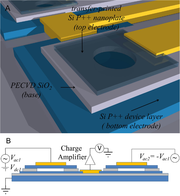
Figure 1. (A) Illustration of the device. (B) Cross-sectional view showing the electrical scheme used to enable the electrostatic actuation of the plate and the capacitive detection of its resonance frequency.
Three important parameters were considered in the device design: the cavity (i.e. resonating plate) radius r, the plate thickness t, and the gap height h. In terms of electrical detection, it is favorable to increase the device capacitance by maximizing r and minimizing h. In terms of vibration mechanics, minimizing r and maximizing t lead to an increase of the resonance frequency of the device and thus of its Q factor. However, one needs to keep in mind that the device resonant frequency cannot exceed the bandwidth of the measurement electronics. In terms of fabrication, it is preferable to minimize r and maximize h and t. Indeed, thinner and larger plates can be difficult to transfer print and are prone to buckling because of compressive stress induced during the high-temperature sealing process. To best satisfy the aforementioned considerations, we have thus selected the following trade-off values: a gap height h = 200 nm, a plate thickness t = 340 nm, and a cavity radius r between 8 and 20 μm (Bhaswara et al., 2014).
Materials and Methods
Device Fabrication
The fabrication process of the device is illustrated in Figure 2. Two silicon-on-insulator (SOI) wafers were used as starting substrates to fabricate the nanoplate resonators: first, a 0.34/1/500-μm thick P-type wafer (from BT electronics) was used as the donor substrate; second, a 2/1/500-μm thick P++-type wafer (from BT electronics) was used as the acceptor substrate. The donor SOI wafer was further doped with boron at a dose of 106 atoms/cm2, followed by thermal annealing at 1000°C during 20 min in order to reduce the electrical resistance of the top layer. Low resistance top layers for both donor and acceptor wafers were necessary in order to use silicon directly as top and bottom electrodes of the device.
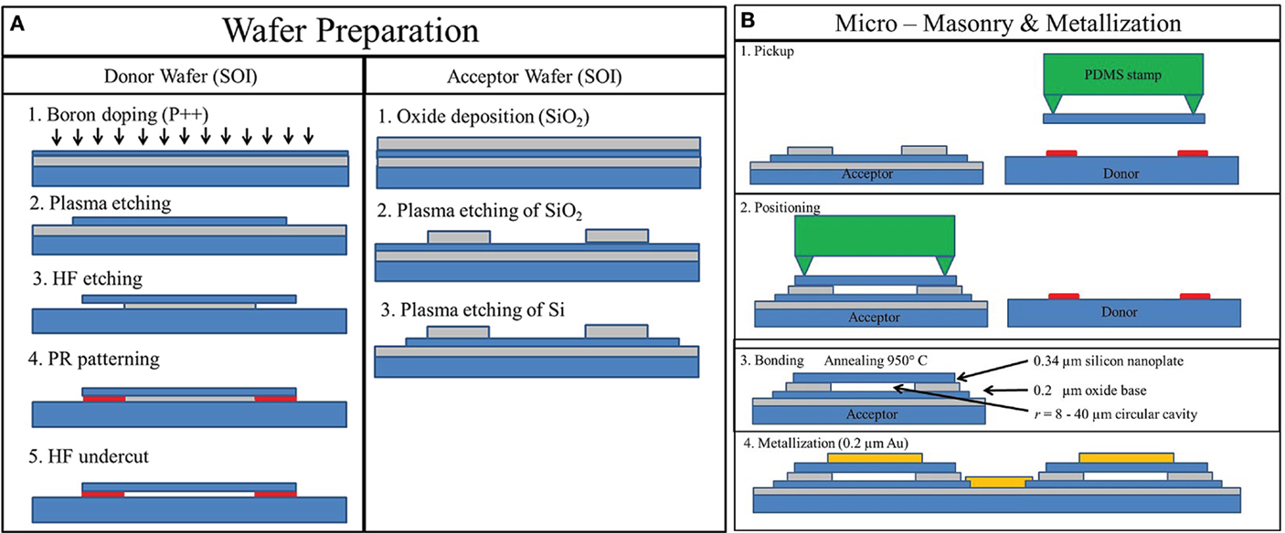
Figure 2. Fabrication process involving (A) the preparation of both donor and acceptor substrates and (B) the micro-masonry step used to transfer and bond nanoplates onto base structures followed by metallization to create interconnect lines.
The nanoplate inks were fabricated from the donor wafer as follows. First, 100 μm × 100 μm squares were patterned using photolithography to define the ink shapes in the silicon device layer. Then, dry reactive ion etching (RIE) was performed to form the nanoplates that remained attached to the buried oxide layer. Subsequently, HF solution was utilized to remove the unnecessary box oxide layer as well as a small region beneath the silicon nanoplates. This undercut region was filled with PR followed by complete removal of oxide layer resulting in suspended nanoplates with PR anchors. The suspended nanoplates were then transfer printed through micro-masonry, leaving PR anchors behind on the donor substrate. The thickness of the silicon nanoplate ink was defined by the thickness of the top silicon layer of the SOI donor wafer (0.34 μm in our case).
The acceptor chips were fabricated from the acceptor wafer as follows. First, a 200-nm thick PECVD oxide layer was deposited at 300°C, 1 mbar on top of a bulk silicon wafer. Then, the base structure was patterned using photolithography followed by RIE. The base structures consisted of square shapes (120 μm side lengths) with one or more circular cavities with radius r ranging from 8 to 20 μm. Base structures with multiple cavities resulted in multiple nanoplate devices obtained in a single transfer-printing step, thus enabling a parallel fabrication capability. Another lithography step followed by RIE was carried out to separate the bottom electrodes below each base structure in order to electrically address them separately. Finally, and prior to the transfer printing of the ink onto the base structure, the receiver wafer was diced into 1 cm × 1 cm chips.
Transfer printing of the silicon nanoplate inks was achieved by means of PDMS microtip stamps (Kim et al., 2010; Keum et al., 2012). These stamps have pyramidal tips that provide suitable adhesion force to enable the pickup and the printing steps. While the transfer printing of Si layers onto SiO2 surfaces was previously demonstrated (Keum et al., 2012), the nanometer thick Si layer suspended above the cavity is prone to buckle during high-temperature annealing process due to the differences in thermal expansion coefficients, thus possibly leading to the delamination of the nanoplate. In order to improve adhesion between the Si layer and the SiO2 base, the base was exposed to O2 plasma prior to transfer printing of the Si nanoplates (Suni et al., 2002). On the surface-activated SiO2 base substrate, the inks were aligned and transferred using appropriate speed and force profiles. A manual stage equipped with an optical microscope was utilized to manipulate the donor substrate while the stamp was stationary under the microscope. Afterwards, the nanoplates were pressed along the circumference of the cavities to ensure good contact using a single tip stamp. The chip was finally annealed at 600°C to permanently bond the base and the nanoplate. Afterwards, the combined structures underwent metallization to create electrical interconnects to the top electrode (silicon nanoplate, i.e., top silicon layer of the donor wafer) and the bottom electrode (top silicon layer of the acceptor substrate), and to ground the bulk silicon acceptor wafer. In order to do so, Cr and Au layers were evaporated and patterned by lift-off at the single chip level. For packaging purposes, each chip was finally wire-bonded and mounted onto a specifically designed and fabricated printed circuit board (PCB). Typical fabricated devices are shown in Figure 3: the device on the right-hand side with double cavities of radius r = 14 μm is the actual active resonator, while the device shown on the left-hand side is used as a reference for appropriate capacitance compensation.
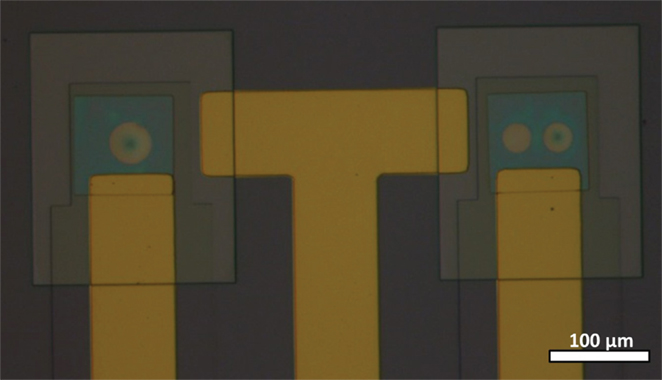
Figure 3. Optical microscope image of fabricated nanoplate resonators. The active device is the one shown on the right-hand side, displaying double cavities with r = 14 μm. The device shown on the left-hand side with r = 20 μm is used as a reference for the capacitive measurement.
Measurement Method
Figure 4 shows the equivalent circuit of a paired device (active and reference resonators), as well as the configuration of voltage bias at each port. The charges flowing through device 1 (active device), represented by the parasitic capacitance Cp1 and the resonator capacitance C1(t), and driven by a combination of AC bias Vac1 and DC bias Vdc1 is expressed by (Trusov and Shkel, 2007)
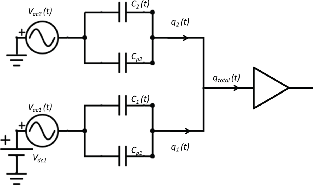
Figure 4. Schematics of the measurement scheme used for a paired device.
The second term of the equation with C1(t) contains the information about the resonator movement, while the first term of the equation concerns the static capacitance of the device, the parasitic effects of the oxide layer between the electrodes, and the parasitic capacitance of the silicon and the metal interconnects. This parasitic term is orders of magnitude larger than the measurement signal (actually about two orders of magnitude for the presented device) and must be properly removed before final signal amplification.
In this measurement scheme, compensation is achieved by driving device 2 using an AC voltage bias Vac2 close in magnitude to Vac1 but with an opposite phase. Devices 1 and 2 are geometrically symmetrical except for the number and size of the cavities, thus they have identical parasitic capacitance value and Cp1 = Cp2 = Cp. Since devices 1 and 2 were designed with different resonant frequencies, C2(t) can be considered constant with respect to time when C1(t) varies with time around its resonance, and vice versa. Thus, we can neglect the effect of C2(t) around the resonant frequency of device 1, and the charges flowing out of device 2 is
Since
the total charges qtotal, feeding the amplifier is
This quantity of charges was then amplified using a charge amplifier and fed into a network analyzer. The resulting data were subtracted with the background signal at Vdc1 = 0 V and filtered using the moving average method to remove the noise.
In addition to the integrated capacitive detection measurements, optical detection of the resonant frequency of the active devices was achieved using a Fabry–Perot setup for comparison means (Bhaswara et al., 2014). The center of each nanoplate was chosen as the optical measurement spot, since it corresponds to the maximum amplitude of the first vibration mode of a circular plate. To reflect typical sensor working conditions, characterizations were carried out under atmospheric pressure at room temperature unless stated otherwise.
Results and Discussion
The frequency response of a fabricated device displaying two cavities with r = 14 μm (Figure 3) under Vdc1 ranging from 0 to 3.5 V and Vac1 of 0.22 V obtained using optical and capacitive sensing is shown in Figures 5A,B, respectively. The resonant peaks corresponding to fundamental modes of the two cavities can be observed using both optical and capacitive methods. The difference in resonant frequency between the supposedly identical cavities is expected to come from process variation, which might result in slightly different geometries and intrinsic stress inside the plate.
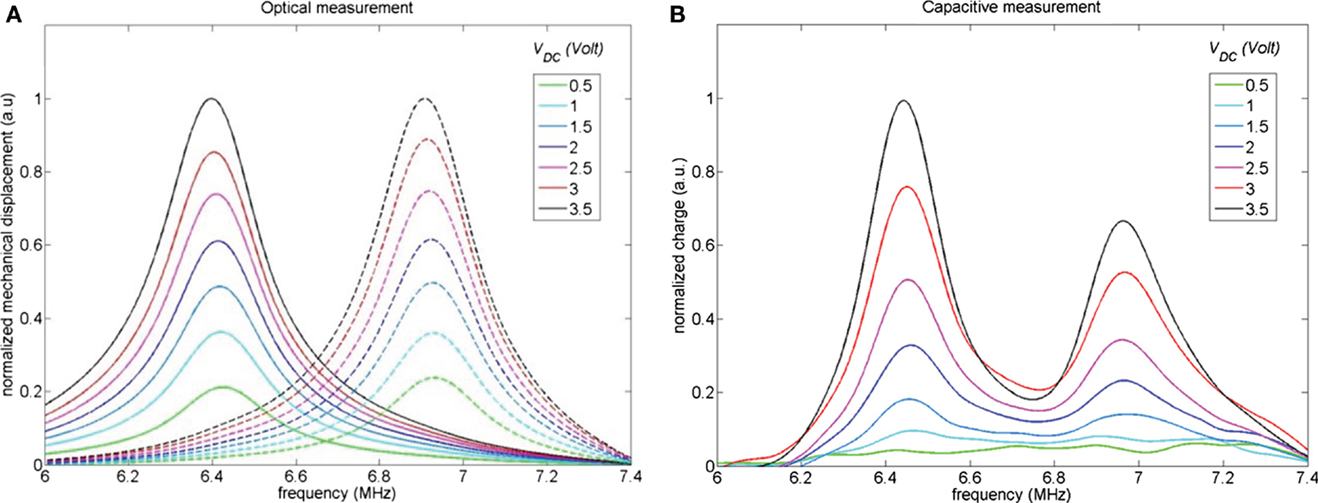
Figure 5. Frequency response of the device obtained using (A) optical Fabry–Perot sensing and (B) capacitive sensing.
For the optical characterization response, which is proportional to the displacement of the resonator, peaks can still be detected at Vdc1 = 0.5 V and even at Vdc1 = 0 V due to presence of a DC offset within the device. The value of this DC offset is Voffset = 0.32 V, which was determined by adjusting the DC bias until the peak value fell down under the noise level of the measurement device. For capacitive sensing method, which senses the vibrations of both cavities simultaneously, distinct peaks can be distinguished starting at Vdc = 1.5 V, below which no clear resonant peaks can be observed.
The normalized mechanical displacement and the normalized output charge for one of the cavities is shown in Figure 6 as a function of Vdc1 (empty and filled red circles, respectively). While in general, the amplitude of the circular plate capacitor is a non-linear function of Vdc1 (Ahmad and Pratap, 2010), the displacement of the device is small enough so that the experimentally measured amplitude is observed to be linear up to a DC bias value of 3.5 V. However, the output charge is observed to vary with the square of Vdc1. Looking back into Eq. 4, it can be observed that qtotal(t) is proportional to only if C1(t) is proportional to Vdc1, which, similarly to the case of the amplitude vibration, is true only for small displacements. Thus, both optical and capacitive measurements show that the device behavior is consistent with what is expected for parallel plate capacitors in the linear regime for Vdc1 values between 0.5 and 3.5 V.
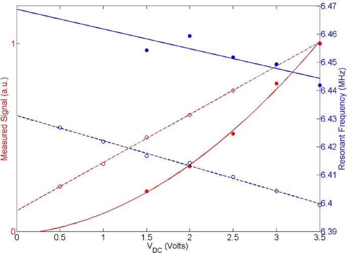
Figure 6. Graph describing the variation of peak height (red) and resonant frequency (blue) with Vdc1 using both optical (empty circles) and capacitive (filled circle) sensing methods. The guiding lines are plotted using a linear curve fit, with the exception of the solid red line that uses a quadratic curve fit. The graph corresponds to the response given by the first cavity of the device, with fundamental resonant frequency, f0, value of around 6.44 MHz.
The variation of resonant frequency with Vdc1 for the first cavity is shown in Figure 6 for both optical and capacitive sensing (empty and filled blue circle, respectively). Comparison between the two sensing methods shows that optical measurement gives rise to a lower resonant frequency value (around 45 kHz lower) compared to capacitive sensing. This can be attributed to the local heating of the device by the laser beam used in the Fabry–Perot setup, which causes both compressive thermal stress within the structure and change in the silicon’s Young modulus that reduces the resonant frequency. For both sensing methods, it can be observed that the resonant frequency decreases linearly and inversely with Vdc1. The optical sensing method shows that between Vdc1 = 0.5 and 3.5 V, the resonant frequency is reduced by 27.5 kHz, while the capacitive sensing method shows that between Vdc1 = 1.5 and 3.5 V, the resonant frequency is reduced by 12.5 kHz. The frequency decrease appears to be linear, which suggests influence from both spring softening effect as commonly observed in capacitive devices (Seeger and Boser, 2003), and tensile stress on the plate due to the DC bias applied between the electrodes.
The analytical value for the first mode resonant frequency of a circular clamped plate is (Schomburg, 2011)
where r is the plate radius, t the plate thickness, ρ the density of material, ν the Poisson’s ratio, E the Young’s modulus, and σ0 the in-plane stress in the plate. Assuming no stress, substituting silicon mechanical properties for plate bending (ρ = 2329 kg m−3, E = 170 GPa, and ν = 0.064) and r = 14 μm, t = 0.34 μm into Eq. 5 yields an analytical resonant frequency fanalytical value of 7.05 MHz, which is pretty consistent with the values obtained from optical and capacitive measurements. Still, the lower experimental resonant frequency values indicate the presence of tensile stress within the plate, which can be determined using Eq. 5:
Substituting fexperimental = 6.44 and 6.96 MHz for the first and second devices yields the in-plane stress values of σ0 = −22.2 and −3.4 MPa, respectively. These values are comparable with results obtained in our previous work (Bhaswara et al., 2014) and are representative of typical stress values and resonance frequency variations involved with the micro-masonry process.
For a further assessment of the structure’s performances, we have finally compared the device behavior in atmospheric pressure and vacuum. Figure 7 shows the frequency response of one of the devices both in atmospheric pressure (P = 1012 mbar) and in vacuum (P = 1.2 mbar) obtained using optical sensing. The Q factor of the device at atmospheric pressure is determined to be Qair = 33. In vacuum, the Q factor was determined to be Qvacuum = 77, which is much lower compared to the values obtained from our previous work (Qvacuum = 3000) (Bhaswara et al., 2014). This result suggests that a pocket of air exists in the gap between the plate and the substrate even when the measurement chamber is under vacuum, and the seal between the plate and the base structure is thus hermetic. For information, our previous structures exhibited vents within the base structure, thus allowing pressure under the plate to equilibrate the working pressure (Bhaswara et al., 2014). While this results in lower Qvacuum, this does not significantly affect operation in air, and the tight seal will prove advantageous in liquid environment. This also means that our presented process that relies on micro-masonry for the fabrication of nanoplate structures could also be used for obtaining devices with vacuum pockets, which might potentially find applications, e.g., pressure sensors or biosensors.
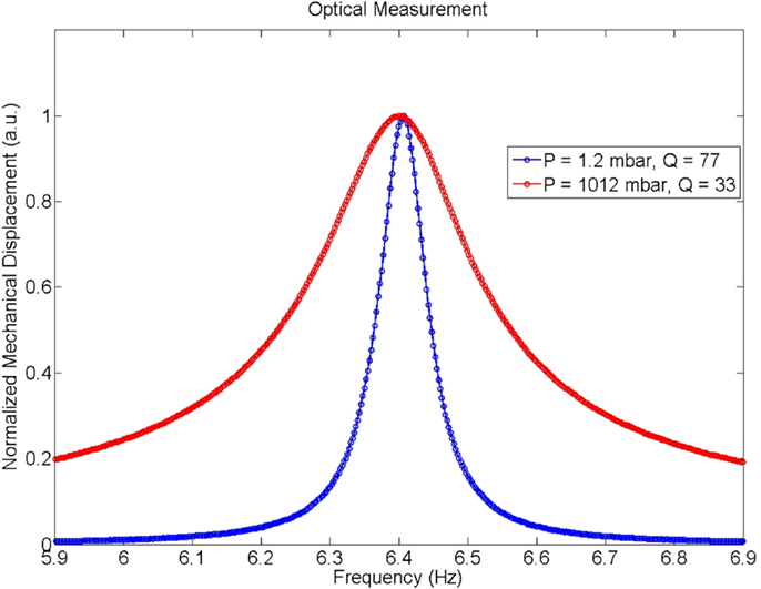
Figure 7. Frequency response of the first cavity in vacuum (blue line, P = 1.2 mbar, Qvacuum = 77) and in atmospheric pressure (red line, P = 1012 mbar, Qair = 33). The amplitude of both curves has been normalized due to difference in optical measurement setup.
Conclusion
We have successfully fabricated nanoplate resonators with integrated actuation and sensing schemes using micro-masonry. This method was used to fabricate devices with 200-nm-thick air gaps without structure collapsing due to stiction. We have demonstrated that the resulting structure is robust enough to withstand post-processing (e.g., metallization and lift-off processing). The fabricated device was driven at its resonant frequency using electrostatic actuation, and the vibration amplitude detection of multiple resonators was performed using both capacitive and optical sensing. The device exhibits behavior consistent with parallel plate capacitor device theory for small displacements. Compressive stress within the plate was determined to be between 3 and 20 MPa, which is comparable with values obtained in the previous works. Comparison of device Q factor in vacuum and atmospheric pressure suggests that the bond between the base and the plate is airtight.
Author Contributions
TL, LN, and SK conceived the research; AB designed and characterized the nanoplates; AB, and HK fabricated the nanoplates; FM designed and fabricated the associated electronics; and BL helped with electrical characterization and data analysis.
Conflict of Interest Statement
The authors declare that the research was conducted in the absence of any commercial or financial relationships that could be construed as a potential conflict of interest.
Funding
The authors gratefully acknowledge the INSIS-CNRS financial support NANOBIOD-2013 and the NSF financial support CMMI-1351370. This work was partly supported by the French RENATECH network.
References
Ahmad, B., and Pratap, R. (2010). Elasto-electrostatic analysis of circular microplates used in capacitive micromachined ultrasonic transducers. IEEE Sens. J. 10, 1767–1773. doi: 10.1109/JSEN.2010.2049017
Alava, T., Mathieu, F., Mazenq, L., Soyer, C., Remiens, D., and Nicu, L. (2010). Silicon-based micromembranes with piezoelectric actuation and piezoresistive detection for sensing purposes in liquid media. J. Micromech. Microeng. 20, 075014. doi:10.1088/0960-1317/20/7/075014
Aslam, M. (2013). Bulk etching of silicon wafer and development of a polyimide membrane. J. Phys. Conf. Ser. 439, 012029. doi:10.1088/1742-6596/439/1/012029
Bhaswara, A., Keum, H., Rhee, S., Legrand, B., Mathieu, F., Kim, S., et al. (2014). Fabrication of nanoplate resonating structures via micro-masonry. J. Micromech. Microeng. 24, 115012. doi:10.1088/0960-1317/24/11/115012
Carlson, A., Bowen, A. M., Huang, Y., Nuzzo, R. G., and Rogers, J. A. (2012). Transfer printing techniques for materials assembly and micro/nanodevice fabrication. Adv. Mater. 24, 5284–5318. doi:10.1002/adma.201201386
Ergun, A., Yaralioglu, G., and Khuri-Yakub, B. (2003). Capacitive micromachined ultrasonic transducers: theory and technology. J. Aerosp. Eng. 16, 76–84. doi:10.1061/(ASCE)0893-1321(2003)16:2(76)
Ismail, A. K., Burdess, J. S., Harris, A. J., McNeil, C. J., Hedley, J., Chang, S. C., et al. (2006). The principle of a MEMS circular diaphragm mass sensor. J. Micromech. Microeng. 16, 1487. doi:10.1088/0960-1317/16/8/008
Keum, H., Carlson, A., Ning, H., Mihi, A., Eisenhaure, J. D., Braun, P. V., et al. (2012). Silicon micro-masonry using elastomeric stamps for three-dimensional microfabrication. J. Micromech. Microeng. 22, 055018. doi:10.1088/0960-1317/22/5/055018
Kim, S., Wu, J., Carlson, A., Jin, S. H., Kovalsky, A., Glass, P., et al. (2010). Microstructured elastomeric surfaces with reversible adhesion and examples of their use in deterministic assembly by transfer printing. Proc. Natl. Acad. Sci. U.S.A. 107, 17095–17100. doi:10.1073/pnas.1005828107
Lu, X., Guo, Q., Xu, Z., Ren, W., and Cheng, Z.-Y. (2012). Biosensor platform based on stress-improved piezoelectric membrane. Sens. Actuators A Phys. 179, 32–38. doi:10.1016/j.sna.2012.03.004
Mastrangelo, C. H., and Hsu, C. H. (1993). Mechanical stability and adhesion of microstructures under capillary forces. I. Basic theory. J. Microelectromech. Syst. 2, 33–43. doi:10.1109/84.232593
Rollier, A.-S., Legrand, B., Collard, D., and Buchaillot, L. (2006). The stability and pull-in voltage of electrostatic parallel-plate actuators in liquid solutions. J. Micromech. Microeng. 16, 794. doi:10.1088/0960-1317/16/4/016
Schomburg, W. K. (2011). Introduction to Microsystem Design. Berlin; Heidelberg: Springer. Available at: http://link.springer.com/10.1007/978-3-642-19489-4
Seeger, J. I., and Boser, B. E. (2003). Charge control of parallel-plate, electrostatic actuators and the tip-in instability. J. Microelectromech. Syst. 12, 656–671. doi:10.1109/JMEMS.2003.818455
Suni, T., Henttinen, K., Suni, I., and Mäkinen, J. (2002). Effects of plasma activation on hydrophilic bonding of Si and SiO2. J. Electrochem. Soc. 149, G348–G351. doi:10.1149/1.1477209
Tas, N., Sonnenberg, T., Jansen, H., Legtenberg, R., and Elwenspoek, M. (1996). Stiction in surface micromachining. J. Micromech. Microeng. 6, 385. doi:10.1088/0960-1317/6/4/005
Trusov, A. A., and Shkel, A. M. (2007). Capacitive detection in resonant MEMS with arbitrary amplitude of motion. J. Micromech. Microeng. 17, 1583. doi:10.1088/0960-1317/17/8/022
Vishwakarma, S. D., Pandey, A. K., Parpia, J. M., Southworth, D. R., Craighead, H. G., and Pratap, R. (2014). Evaluation of mode dependent fluid damping in a high frequency drumhead microresonator. J. Microelectromech. Syst. 23, 334–346. doi:10.1109/JMEMS.2013.2273803
Keywords: resonator, MEMS/NEMS, electrostatic actuation, capacitive detection, micro-masonry
Citation: Bhaswara A, Keum H, Mathieu F, Legrand B, Kim S, Nicu L and Leïchlé T (2016) A Simple Fabrication Process Based on Micro-masonry for the Realization of Nanoplate Resonators with Integrated Actuation and Detection Schemes. Front. Mech. Eng. 2:1. doi: 10.3389/fmech.2016.00001
Received: 12 November 2015; Accepted: 10 February 2016;
Published: 01 March 2016
Edited by:
Oscar Vazquez Mena, University of California Berkeley, USAReviewed by:
Qin Zhou, University of California Berkeley, USASchahrazède Mouaziz, École Polytechnique Fédérale de Lausanne, Switzerland
Copyright: © 2016 Bhaswara, Keum, Mathieu, Legrand, Kim, Nicu and Leïchlé. This is an open-access article distributed under the terms of the Creative Commons Attribution License (CC BY). The use, distribution or reproduction in other forums is permitted, provided the original author(s) or licensor are credited and that the original publication in this journal is cited, in accordance with accepted academic practice. No use, distribution or reproduction is permitted which does not comply with these terms.
*Correspondence: Liviu Nicu, nicu@laas.fr;
Thierry Leïchle, tleichle@laas.fr