Coulomb blockade phenomena observed in supported metallic nanoislands
- 1Faculté des Sciences de Base, Ecole Polytechnique Fédérale de Lausanne, Institut de Physique de la Matière Condensée, Lausanne, Switzerland
- 2Key Laboratory for Physics and Chemistry of Nanodevices and Department of Electronics, Peking University, Beijing, China
- 3Institut des Nanosciences de Paris, Université Pierre et Marie Curie and CNRS-UMR 7588, Paris, France
- 4Department of Chemical Physics, Fritz-Haber-Institute of the Max-Planck-Society, Berlin, Germany
The electron transport properties of single crystalline metallic nanostructures in the Coulomb blockade (CB) regime have been investigated by low-temperature scanning tunneling spectroscopy. To this end, nanoscale flat-top Pb islands with well-defined geometries are grown on NaCl-covered Ag(111) substrates. The tunneling spectra acquired at 4.6 K on the Pb nanoislands reflect the presence of single electron tunneling processes across the double-barrier tunnel junction (DBTJ). By a controlled change of the tip-island tunnel distance, the spectra display the characteristic evolution from CB to Coulomb staircase (CS) regime. Simulations within the semi-classical orthodox theory allow us to extract quantitatively the parameters characterizing the DBTJ, i.e., the resistances, capacitances, and the residual charge Q0. Manipulation of Q0 is achieved by controlled application of voltage pulses on the Pb islands. Moreover, under specific tunneling conditions, the influence of the tip-island junction on Q0 is revealed in topographic images of the Pb islands.
1. Introduction
The study of Coulomb blockade (CB) phenomena in nanostructures is a very attractive area of condensed matter physics, because single electron electronics is considered to have a high potential for basic research and for technological applications (1–5). The field started more than 40 years ago with the investigation of small metal particles embedded in an oxide layer between two planar metal electrodes (6, 7). Subsequently, in order to avoid ensemble effects and to study single double-barrier tunnel junctions (DBTJ), CB phenomena have been investigated in small-area tunnel junctions prepared by lithographic methods developed for microelectronics (8, 9). More recently, junctions using a scanning tunneling microscope (STM) tip as one adjustable electrode came into the focus of research (10–13).
Consider single electron transport in the system shown in Figure 1: the two barriers constitute a DBTJ. For each junction the barriers are modeled by an ohmic resistor Ri in parallel with a capacitor Ci, i = 1 for the substrate-island junction and i = 2 for the island-tip junction, as shown in the equivalent electronic circuit in Figure 1B. In order to transfer a single electron through the DBTJ, the electron must overcome the Coulomb charging energy Ec = e2/C∑, where C∑ = ΣCi. If the charging energy Ec is much larger than the thermal energy kBT, the tunneling of an electron is blocked for bias voltages smaller than Uc = e/C∑. This phenomenon has been termed CB (CB) (2, 3, 14–16). Moreover, in order to keep charge fluctuations sufficiently small, the coupling resistance of each junction has to be significantly larger than the quantum resistance: Ri ≫ RQ = h/(2e2) ≈ 12.9 kΩ. These conditions imply that extremely small metal clusters have to be probed, or that the measurements have to be performed at low temperature.
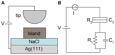
Figure 1. (A) Schematic diagram of the Coulomb blockade system. The Pb nanoisland is embedded between the vacuum barrier and a few NaCl dielectric layers on Ag(111). (B) Equivalent double-barrier tunnel junction (DBTJ) circuit where each junction is represented by a set of capacitors and resistors, connected in parallel.
Previous studies of nanostructures in the CB regime by STM were performed on amorphous particles (11, 13, 17, 18), on particles covered by shells consisting of specific ligands and/or molecules (19–22), and to a lesser extent on supported clusters and metal islands (18, 23–26). The vast majority of the CB spectroscopy results have been successfully described within the orthodox theory of the DBTJ (2), which allowed the authors to determine quantitatively the tip-particle and the particle-substrate junction parameters (see Figure 1B). Within the context of single electron tunneling, the “orthodox theory,” a semi-classical theory, is based on the following three assumptions (3). (1) The electron energy quantization inside the conductors is ignored, i.e., the electron energy spectrum is continuous. (2) Coherent quantum processes consisting of several simultaneous tunneling events (“cotunneling”) are ignored. This assumption is valid if the resistance of all tunneling barriers of the system is much higher than the quantum unit of resistance. Only under this condition the quantum-mechanical uncertainty of electrons is suppressed because of the high tunneling resistance (i.e., less tunneling events). Thus one can neglect the concurrent tunneling events and treat one electron at a time, which makes controllable single-electron manipulation possible. (3) The tunneling time τt of an electron tunneling through the barrier is assumed to be negligible compared to other time scales (including the interval between subsequent tunneling events). For a typical tunneling event in a practical junction (3), τt is around 10−15 s. For a typical STM tunneling junction with 1 nA tunneling current, on average one electron tunnels per 10−10 s. Considering that the electronic lifetime of an electron in the states of the islands is around 10−13−10−15 s, electrons tunnel one at a time and consequently under these conditions cotunneling processes can be neglected.
Recently, in a low-temperature scanning tunneling spectroscopy (STS) study, we reported (27) on the observation of the dynamical Coulomb blockade (DCB) (28–30) in nanosized electrical contacts consisting of small Pb islands on various conducting, semiconducting, and partially insulating substrates. We observed a suppression of the differential tunnel conductance at small bias voltages due to DCB effects. The differential conductance spectra allowed us to determine the capacitances and resistances of the electrical contact which depend systematically on the island-substrate contact area. Calculations based on the theory of environmentally assisted tunneling agree well with the measurements.
Here, we extend the previous observations from the DCB to the orthodox CB and Coulomb staircase (CS) regime. We report on the observation of CB phenomena in Pb nanoislands, ranging from a lateral size of a few nanometers to tens of nanometers and a thickness of a few monolayers, grown on ultrathin dielectric films of NaCl deposited on Ag(111). For selected Pb islands of well-defined area, the local tunneling spectra reflect CB and CS phenomena in the DBTJ (see Figure 1) characteristic for single electron tunneling: Every additional electron tunneling to or from the Pb nanoisland is counted one by one. Using a model based on the orthodox theory of single electron tunneling (12, 16), we are able to simulate the experimental tunneling spectra and to extract the relevant parameters of the DBTJ, i.e., the resistances of island-substrate and tip-island junctions (R1 and R2), the capacitances of island-substrate and tip-island junctions (C1 and C2), and the residual charge (Q0) on the island. The extracted C1 capacitances fit well with the values corresponding to a planar capacitor, C1 = ε0 εrAisland/d, the island area Aisland being measured from the STM topography and the insulator thickness determined by field emission resonances (FERs) analysis. Manipulation of Q0 is achieved by controlled application of voltage pulses on the Pb islands. Moreover, under specific tunneling conditions, the influence of the adjustable tip-island junction on Q0 is revealed in topographic images of the Pb islands.
In an STM measurement of a DBTJ, in general the tip-island junction resistance R2 is always much larger than the quantum resistance RQ. Then the electron transport through such a DBTJ can be separated into three different regimes (16): if the island-substrate resistance R1 ≪ RQ, the whole system corresponds to a single junction; if R1 is of the order of RQ, the dynamical Coulomb blockade (DCB) regime is reached; if R1 ≫ RQ, the CB and CS regime is entered. These different conditions can be selectively and controllably fulfilled in our experimental setup by choosing the appropriate size of the islands (by changing the growth parameters) and the pertinent tunnel parameters, including an adjustable tip-island distance (by changing the tip-island resistance R2). In this way island-size-dependent CB gaps and CS have been unambiguously identified in the tunneling spectra obtained on the Pb quantum dots on NaCl/Ag(111).
2. Experimental
The Ag(111) single crystal substrate was cleaned by Ar+ sputtering and subsequent annealing cycles. NaCl powder was thermally evaporated from a crucible at a temperature of T = 620 °C onto the Ag substrate held at room temperature or heated to ≈ 420 K. Subsequently, Pb islands were grown by evaporation of Pb from a W filament onto the NaCl-covered Ag substrate cooled to 130 K to obtain Pb islands of the desired size.
The experiments were conducted in a homebuilt STM operated at 4.6 K (31). Differential conductance (dI/dV) measurements were performed with an open feedback loop using a lock-in technique with modulation voltage from 2 to 10 mVpp at 300–400 Hz frequency with tunneling current ranging from 100 pA to a few nA.
3. Results and Discussion
3.1. Growth of Pb Nanoislands on NaCl/Ag(111)
A bulk NaCl crystal is a dielectric material with a wide band gap in the range of 8.5 − 9 eV (32–34). For thin NaCl films, the band gap is reported to be close to the bulk value (35) For 1 − 3 ML of NaCl on Ag(100), recent STS measurements of the energy positions of field emission resonances propose a work function of 3.2 eV (36), while ultraviolet photoemission spectroscopy (UPS) yields 3.5 eV (36, 37). From dI/dV spectra measured on top of a 2 ML NaCl film, we deduce that the gap lies within the voltage range of ± 2 eV around EF, which is the energy range selected for the measurement of the dI/dV spectra of the Pb nanoislands on NaCl.
Studies of NaCl layers on other substrates abound, e.g., on Al(111) (35, 38), on Cu(111) (39), on Ag(100) (36, 40, 41), and on Au(111) (42–44). NaCl(100) layers are very versatile as a dielectric ultrathin film for the electronic decoupling of supported molecules (39, 42, 43) or other nanostructures (27) from a metallic substrate.
Here, NaCl was deposited on the substrate held at two different temperatures, 300 K, and ≈ 420 K, the latter favoring the formation of more extended, flatter, and defect-free layers. Figures 2A,B show STM images corresponding to these two different sample preparations, yielding Pb islands of different average size. This behavior is mainly due to the higher density of nucleation points on the NaCl layer in (b) with respect to (a). The NaCl layer has different characteristics in the two cases: the layer is flat and presents very few defect in (a), while it shows the coexistence of various thicknesses and a higher density of edges in (b). In (a) the side length of the equilateral triangular Pb islands is in the range of 25 to 60 nm, while in (b) it is ≤ 10 nm. For the STS measurements, triangular islands of various sizes were selected. The Pb islands expose (111) crystal faces. A determination of the thickness of NaCl layers at a given location is not straightforward. Moreover, the apparent height of NaCl layers varies depending on tunneling conditions, such as bias voltage and tip conditions.
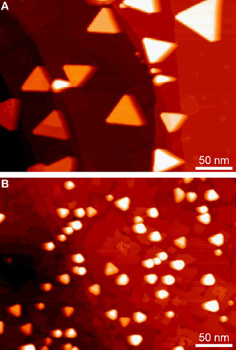
Figure 2. STM topographies acquired on two different samples with Pb islands grown on NaCl/Ag(111). Pb islands are visible in both images, most of them with triangular shape and a few with rounded shape. The smaller island size in (B) as compared to (A) is obtained on a NaCl film exhibiting more defects. (A): +1 V, 20 pA; (B): +4 V, 20 pA.
3.2. Coulomb Blockade and Coulomb Staircase on Pb Nanoislands
In a STM double junction geometry, there are some intrinsic limitations in the relations between resistances and capacitances of the two junctions. As discussed in the introduction, in order to observe CB phenomena, the condition Ri ≫ RQ has to be satisfied. In the tunneling regime, this condition is easily satisfied for junction 2 (tip-vacuum-island), for which resistances R2 of 1 MΩ to 1 GΩ are usual. For junction 1, this condition requires the presence of an insulating layer of sufficient thickness, leading in our case to resistances R1 of the order of 1 MΩ to 100 MΩ. Concerning the capacitance, although the tip-island distance is of the same order as the insulating layer thickness (0.5 to 1 nm), the NaCl dielectric constant plays an important role, leading to capacitances C1 ten times larger than typical values for C2. By varying the set-point current, the tip-island distance is modified and consequently also R2 and C2. The resistance, however, decreases exponentially with decreasing distance, while the capacitance increases only weakly.
Figure 3 shows dI/dV spectra acquired on four different Pb islands. The spectra present the typical signature of CB, i.e., a zero-conductance gap around the Fermi energy (EF). Notice that bulk Pb is superconducting at the measurement temperature of T = 4.6 K. We neglect here the possible existence of the superconducting gap in the Pb islands because the energy scale of the Coulomb gap is much larger than the one of the superconducting gap of ≤ 1 meV (45). Consequently, we treat the tunneling junctions as if they are in the normal state. The width of the gap is inversely proportional to the island area Aisland: the gap is ≈ 120 mV wide for the smallest island (Aisland ≈ 20 nm2), and ≈ 18 mV for the largest one (Aisland ≈ 220 nm2). This is the expected behavior, since for C2 < C1 the gap width is governed by the tip-substrate capacitance C1. Therefore, as C1 increases for increasing island area, it leads to narrower gaps. The 220 nm2-island (a triangle with 22 nm side) represents the upper limit for an unambiguous observation of a zero-conductance gap at this temperature. From the measured gap, we estimate C1 to approximately 10 aF. For the 20 nm2-island, C1 is ten times smaller. These values are in agreement with values calculated using the expression for a parallel plate capacitor C1 = ε0 εrAisland/dNaCl, with the island supported on a 3 ML NaCl film of thickness dNaCl = 0.8 nm and dielectric constant of bulk NaCl εr = 5.5 (46) The small features in Figure 3A just below ± 0.1 eV are related to the capacitance C2 (see discussion of Figure 5).
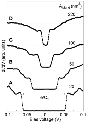
Figure 3. dI/dV spectra labeled (A to D) acquired on four Pb islands with different area Aisland. A Coulomb gap of decreasing size is visible in going from spectrum (A to D) reflecting a Coulomb blockade process.
Figure 4 displays the typical evolution of the tunneling spectra from the CB to the CS regime for a selected Pb triangular island with a side length of 14 nm. The dI/dV spectrum A shows a simple Coulomb gap while spectra B to E display a series of equidistant peaks (steps in the I − V characteristics, a CS) with increasing intensity. This progression is achieved by measuring the tunnel spectra with increasing initial current, corresponding to decreasing tip sample separation and decreasing resistance R2, in going from spectrum A to E. Our simulation within the orthodox theory reproduces the general features of the measured spectra revealing CB and CS characteristics. The simulation of these spectra within orthodox theory allows us to extract the pertinent parameters of the double barrier system, i.e., the capacitances and resistances of both junctions, as well as the residual non-integer charge Q0 on the Pb island, see figure caption. Notice that, with decreasing tip-sample distance, R2 decays exponentially, whereas C2 increases linearly (13, 18). As this latter variation is small, C2 is assumed to be constant throughout this series of simulations. To summarize, tunneling spectra on such nanoislands may display a simple CB gap or a CS depending on the parameters of the DBTJ. Well-developed CS's are observed with an asymmetric resistance ratio R2 < R1.
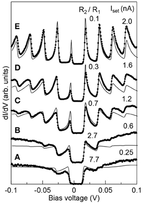
Figure 4. Evolution from Coulomb blockade to Coulomb staircase: experimental STS data acquired on a Pb island with 14 nm side (Aisland ≈ 85 nm2) (dots) and simulation (black line) based on the orthodox theory. The spectra are offset for clarity. Parameters of the simulation: R1 = 39 MΩ, C1 = 7.46 aF, and C2 = 0.7 aF; (A): R2 = 300 MΩ and Q0 = −0.15 e, (B): R2 = 105 MΩ and Q0 = −0.2 e, (C): R2 = 26 MΩ and Q0 = −0.26 e, (D): R2 = 13 MΩ and Q0 = −0.26 e, (E): R2 = 4.5 MΩ and Q0 = −0.28 e.
Concerning the robustness of the simulations and the precision of the derived parameters we note that Q0 is always determined with an error of < 10%, as it corresponds to an energy shift of the tunneling spectra with respect to zero bias voltage. The capacitances C1 and C2 are also reasonably well determined, especially in situations like those depicted in Figure 5 or Figure 6 where two well separated energies are well-defined. The errors of the determined values are thus also < 10%. The sum of R1 and R2 is fixed by the experimentally determined I(V) characteristics. Their ratio is most favorably evaluated in the CS regime, as the height and the width of the various peaks are linked directly to their ratio. In this situation a precision of the order of 10% is obtained (see Figure 4). In the simple CB case, the precision of the resistance ratio is ≥ 10%.
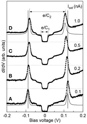
Figure 5. Spectra (A to D): increase of the tip-island capacitance C2 with decreasing tip-island distance (increasing tunnel current). The spectra, offset for clarity as dI/dV(0V) = 0, have been acquired on a Pb island of 14 nm side. Parameters of the simulation, performed for spectra (A) and (D) curve: C1 = 5.0 aF, C2 = 0.77 aF, R1 = 5 MΩ, R2 = 1700 MΩ, Q0 = 0.062 e; (D) curve: C1 = 5.0 aF, C2 = 0.86 aF, R1 = 5 MΩ, R2 = 145 MΩ, Q0 = 0.07 e.
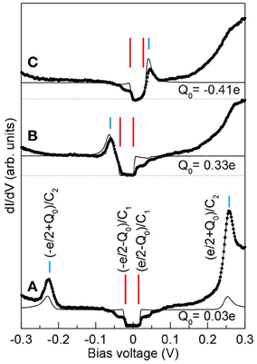
Figure 6. Manipulation of the residual charge Q0. dI/dV spectra measured on the same island with 7.9 nm side, showing features related to both, C1 and C2, with varying Q0, and corresponding simulations. The residual charge (Q0) of the island is changed by a bias voltage pulse (duration: 50 μs, current: 1 nA). Parameters of the simulation: C1 = 3.8 aF, C2 = 0.335 aF, R1 = 25 MΩ, R2 = 2300 MΩ; (A): Q0 = 0.03 e, (B): Q0 = 0.33 e, (C): Q0 = −0.41 e.
A closer comparison of calculations and data in Figure 4 shows that there are some deviations in the intensity of the structures. For the present island of a thickness of 11 ML, a quantum well state, reflecting the vertical confinement, located at +0.2 eV above EF contributes a considerable background to the spectra (47). Therefore, a quantitative fitting of the tunnel spectra within the orthodox theory should consider the density of states (DOS) of the sample (48).
If the parameters of the DBTJ are appropriately chosen, spectral features reflecting both, tip-island (C2) and island-substrate (C1) capacitance can be observed simultaneously. Note that the electrostatic energy of the island is given by the Coulomb charging energy Ec = e2/CΣ, where CΣ = ∑ Ci. However, the threshold voltage necessary for the transfer of an electron across the tip-island (island-substrate) junction is inversely proportional to the capacitance C2 (C1) (12, 13). Spectra of Figure 5 were acquired on a Pb island of ≈ 14 nm side length. Spectrum A shows a Coulomb gap around EF as well as two peaks at ≈ ±0.1 V, which are related to the C2 capacitance. For decreasing tip-island distance (increasing tunnel current), the tip-island capacitance C2 is expected to increase slightly. This behavior is observed in Figure 5B: by approaching the tip to the island from A to D, the value of C2 increases leading to a decreased separation between the two C2 peaks, as indicated by the vertical lines. In addition, if the island area Aisland becomes comparable to the effective tip area Atip, there will be also a contribution to C2 due to the tip-substrate capacitance. In the present measurement Aisland turns out to be smaller than Atip. C2 is then evaluated using the simple parallel-plate capacitance formula. In addition to the capacitance between the metallic island and the tip, the capacitance between the tip and the substrate, including the vacuum and the NaCl layers, is considered in the model.
The present measurements and their analysis allow us to obtain the dielectric constant of the ultrathin NaCl film within a parallel plate capacitor model, if we take the island substrate capacitance C1 from the simulation of the spectra, the area Aisland of the capacitor plate from the STM topographies, and the thickness dNaCl of the NaCl film as deduced from STS of FERs (36) With a typical island size of Aisland = 100 nm2 and dNaCl = 0.8 nm (3 ML), we obtain εr = 4, a reasonable value compared to the one of ε = 5.5 for bulk NaCl (46), and the one extracted from FERs measurements, ε = 3.5 (36).
In contrast to the situation in a planar tunnel junction (49), our setup has no gate electrode. However, by externally applying a bias voltage pulse to the junction (12), a gate voltage change is mimicked. In Figure 6 we present three tunneling spectra, obtained on the same position on a triangular island of 7.9 nm side, where subsequently a bias voltage pulse of ±5 V has been applied to the junction. The spectra clearly show the result of this action, a pulse-bias-dependent shift of the central Coulomb gap away from the symmetric zero-voltage position, accompanied by a shift of the C2-related spectral features. The background above +0.2 V originates from the tail of a quantum well state at higher energy (47). This background contributes also to the observed intensity variations of the spectral features. The asymmetric displacement of the central Coulomb gap and of the C2-related peaks under the action of an external voltage pulse reflects the different values of the fractional residual charge Q0, obtained from our simulation, on the Pb island.
It has been proposed that the residual charge Q0 is related to the difference in work function of the various metals constituting the junctions (12):
where Δϕ1 is the difference between substrate and island work functions, and Δϕ2 the difference between tip and island work functions. As a result of voltage pulses, charge can be trapped in defects or impurities in the NaCl layer beneath the Pb nanoisland, leading to a permanent modification of the residual charge Q0.
In the following section we demonstrate the influence of the tip-island junction on the residual charge Q0 via the variation of C2, variation due to the displacement of the tip with respect to the Pb island during scanning. In Figures 7A,B two different Pb islands are displayed. In the closeup-view topographic images of Figures 7C,D, very striking concentric lines following the contours of the island are visible. Figures 7E,F shows typical dI/dV spectra obtained on these islands. Our measurements show that, by scanning laterally across the surface, an energy shift of the spectrum is observed which corresponds to a maximum fluctuation of the residual charge Q0 = ±e/2. We deduced the Q0 values by simulating each local STS spectrum in the CS regime. For the Pb island shown in Figures 7A,C, we obtain a value of Q0 ≈ +0.35e for the spectrum acquired at the center of the island, and Q0 ≈ −0.15e for the one acquired in the surrounding region. For the system of Figures 7B,D, up to six regions of alternating negative and positive Q0 are detected.
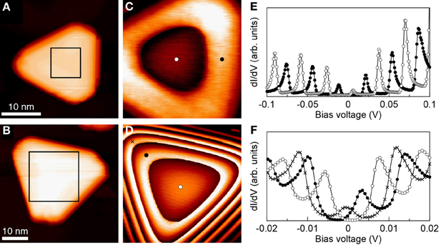
Figure 7. (A,B) Topographic images of Pb islands on NaCl; (A): −1 V, 20 pA, (B): 2.5 V, 20 pA; (C,D) Close-up view; (C): −0.15 V, 200 pA; (D): −0.01 V, 20 pA); (E,F) dI/dV spectra acquired on the locations represented by the corresponding symbol, showing different values of Q0 (see text).
In order to explain this surprising effect we have to consider that the parameters of junction 2 depend on the tip position with respect to the island. As already mentioned, the residual charge Q0 is related to the difference in work function of the various metals constituting the junctions, see Equation 1. For a given set of measurements C1 is fixed by the Pb island and the NaCl layer characteristics and the work functions are well defined. In these conditions, Equation 1 shows that a variation of Q0 can only originate from a variation of C2. As discussed above, the lateral extension of the tip can exceed the island area. Therefore, to evaluate C2, not only the capacitance between tip and island, but also the one between tip and substrate has to be included. When scanning over a Pb island, the ratio between these two contributions changes continuously, leading to variations of the residual charge within the island. Now, considering the CS spectra shown in Figures 7E,F, we recall that with increasing bias voltage every additional CS peak in the differential conductance spectrum indicates the hopping of an additional electron to/from the island. In an STM scan at a bias voltage close to a CS peak, e.g., at 0.075 eV in Figure 7E, a small change in Q0 (due to the changing tip-island capacitance) will lead to a situation where the measurement will be performed above or below the respective CS peak, corresponding to one more (above the peak) or one less electron (below the peak) tunneling to the island. This effect leads to the observed symmetric triangular step patterns in the STM topographies shown in Figures 7A,B. Evidently, the sharp apparent height steps visible in the STM images reflect the hopping of one additional electron on/off the Pb island, while the transition regions correspond to a continuous variation of Q0. Notice that, contrary to the first impression gained from the images, at each instant the value of the charge Q0 is the same over the entire island, as expected for a conducting object. These features are visible when C1Δϕ1 ≈ C2Δϕ2, a condition which can be fulfilled for Δϕ1 ten times smaller than Δϕ2, since C1 is typically ten times larger than C2. This implies that Δϕ1 has to be small in order to observe these features. Moreover, Δϕ2 strongly depends on the specific tip conditions, explaining the fact that these effects were not systematically observed. In this situation, a C2 variation of the order of 10% can induce a modification of Q0 as large as ±e/2.
Finally, we note that the observation of Coulomb charge rings with scanning probe methods has been made before for quantum dots inside carbon nanotubes (50), for quantum dots of a two-dimensional electron gas inside semiconductor heterostructures (51), and for quantum dots inside InAs nanowires (52). Controlled charge switching has been performed for single Au atoms on NaCl (53), for a single Si donor in Si doped GaAs (54), and for a small conductive grain on an InAs surface (55). The present measurements on Pb nanoislands show that these intriguing CB phenomena and the related charging effects are also observed in metallic quantum dots. While the observed phenomena are similar they are not identical. The essential difference between the present measurements and the SPM investigations on the quantum dots before is that in our case the STM tip is in the tunneling mode measuring the conductance through the Pb island without a gate electrode, while the former investigations use a standard conductance measurement of the nanowires (quantum dots) and there the SPM tip represents an external electrode the field of which shifts the CS spectra of the observed quantum dots.
4. Conclusions and Outlook
We investigated the transport properties of single crystalline metallic nanostructures in the CB regime. To this end, small Pb islands with well-defined geometries, ranging from a diameter of a few to tens of nanometers and a thickness of a few monolayers are grown on crystalline NaCl layers on Ag(111) substrate. The tunneling spectra obtained at 4.6 K on the metallic quantum dots show clearly the presence of CB phenomena. By reducing the tip-island distance, the tunneling spectra reflect the evolution from CB to CS. Our simulations employing the semi-classical orthodox theory describe well the observed spectra in both regimes allowing us to extract quantitatively the parameters of the DBTJ, i.e., the resistances, capacitances, and the residual charges.
The present STM/STS studies have shown that not only the size and shape of the metallic nanoislands can be well determined but that, importantly, also their local electronic structure and their transport properties can be quantitatively elucidated. In the past, e.g., the superconducting properties of small particles have been investigated (56) revealing a number parity property. STS experiments of isolated superconducting islands would allow us to observe simultaneously the pairing correlation on islands with different parity. Moreover, in small metallic particles containing magnetic impurities, the Kondo resonance was predicted to be strongly affected in a parity-dependent way (4), another exciting phenomenon to look at with local probes. We believe that STM/STS will continue to be a decisive player for the elucidation of the mesoscopic physics of nanostructures.
Conflict of Interest Statement
The authors declare that the research was conducted in the absence of any commercial or financial relationships that could be construed as a potential conflict of interest.
Acknowledgments
We would like to thank K.-H. Müller and C. Flindt for stimulating discussions. We are also indebted to V. S. Stepanyuk, N. N. Negulyaev, P. Ignatiev, K. Horn and D. Roditchev for their very valuable input. Wolf-Dieter Schneider would like to thank H.-J. Freund for stimulating discussions and for his generous hospitality. We acknowledge financial support of the Swiss National Science Foundation.
References
1. Sohn LL, Kouwenhoven LP, Schön G. Mesoscopic electron transport. Dordrecht: Kluwer Academic Publishers; (1997).
2. Grabert H, Devoret MH, (eds). Single Charge Tunneling. Vol. 294 of NATO ASI Series B: Physics. New York: Plenum Press (1992).
3. Likharev KK. Single-electron devices and their applications. Proc IEEE. (1999) 87:606. doi: 10.1109/5.752518
4. von Delft J, Ralph DC. Spectroscopy of discrete energy levels in ultrasmall metallic grains. Phys Rep. (2001) 345:61. doi: 10.1016/S0370-1573(00)00099-5
5. Aleiner IL, Brouwer PW, Glazman LI. Quantum effects in Coulomb blockade. Phys Rep. (2002) 358:309. doi: 10.1016/S0370-1573(01)00063-1
6. Zeller HR, Giaever I. Tunneling, zero-bias anomalies, and small superconductors. Phys Rev. (1969) 181:789. doi: 10.1103/PhysRev.181.789
7. Lambe J, Jaklevic RC. Charge-quantization studies using a tunnel capacitor. Phys Rev Lett. (1969) 22:1371. doi: 10.1103/PhysRevLett.22.1371
8. Fulton TA, Dolan GJ. Observation of single-electron charging effects in small tunnel-junctions. Phys Rev Lett. (1987) 59:109. doi: 10.1103/PhysRevLett.59.109
9. Iansiti M, Johnson AT, Lobb CJ, Tinkham M. Crossover from Josephson Tunneling to the Coulomb Blockade in Small Tunnel Junctions. Phys Rev Lett. (1988) 60:2414. doi: 10.1103/PhysRevLett.60.2414
10. van Bentum PJM, Smokers RTM, van Kempen H. Incremental Charging of Single Small Particles. Phys Rev Lett. (1988) 60:2543. doi: 10.1103/PhysRevLett.60.2543
11. Wilkins R, Benjacob E, Jaklevic RC. Scanning-tunneling-microscope observations of Coulomb blockade and oxide-polarization in small metal droplets. Phys Rev Lett. (1989) 63:801. doi: 10.1103/PhysRevLett.63.801
12. Hanna AE, Tinkham M. Variation of the Coulomb staircase in a 2-junction system by fractional electron charge. Phys Rev B. (1991) 44:5919. doi: 10.1103/PhysRevB.44.5919
13. Amman M, Field SB, Jaklevic RC. Coulomb -blockade spectrocopy of gold particles imaged with scanning-tunneling-microscopy. Phys Rev B. (1993) 48:12104. doi: 10.1103/PhysRevB.48.12104
14. Kulik IO, Shekhter RI. Kinetic phenomena and charge discreteness effects in granulated media. Sov Phys JETP. (1975) 41:308.
15. Averin DV, Likharev KK. Coulomb Blockade of Single-Electron Tunneling, and Coherent Oscillations in Small Tunnel Junctions. J Low Temp Phys. (1986) 62:345. doi: 10.1007/BF00683469
16. Averin DV, Likharev KK. Mesoscopic Phenomena in Solids. vol. 30 of Modern Problems in Condensed Matter Sciences. Altshuler BL, Lee PA, Webb RA, (eds). Amsterdam: North-Holland; (1991).
17. Oncel N, Hallback AS, Zandvliet HJW, Speets EA, Ravoo BJ, Reinhoudt DN, et al. Coulomb blockade of small Pd clusters. J Chem Phys. (2005) 123:044703. doi: 10.1063/1.1996567
18. Koslowski B, Dietrich C, Weigl F, Ziemann P. Dynamic charging at room temperature of Au nanoparticles prepared by a micellar technique. Phys Rev B. (2007) 75:085407. doi: 10.1103/PhysRevB.75.085407
19. Dubois JGA, Gerritsen JW, Shafranjuk SE, Boon EJG, Schmid G, et al. Coulomb staircases and quantum size effects in tunnelling spectroscopy on ligand-stabilized metal clusters. Europhys Lett. (1996) 33:279. doi: 10.1209/epl/i1996-00333-0
20. Banin U, Cao YW, Katz D, Millo O. Identification of atomic-like electronic states in indium arsenide nanocrystal quantum dots. Nature (1999) 400:542. doi: 10.1038/22979
21. Wang B, Wang H, Li H, Zeng C, Hou JG, Xiao X. Tunable single-electron tunneling behavior of ligand-stabilized gold particles on self-assembled monolayers. Phys Rev B. (2000) 63:035403. doi: 10.1103/PhysRevB.63.035403
22. Wang B, Wang KD, Lu W, Yang JL, Hou JG. Size-dependent tunneling differential conductance spectra of crystalline Pd nanoparticles. Phys Rev B. (2004) 70:205411. doi: 10.1103/PhysRevB.70.205411
23. Andres RP, Bein T, Dorogi M, Feng S, Henderson JI, Kubiak CP, et al. Coulomb staircase” at room temperature in a self-assembled molecular nanostructure. Science (1996) 272:1323.
24. Nilius N, Kulawik M, Rust HP, Freund HJ. Erratum to: quantization of electronic states in individual oxide-supported silver particles [Surface Science 572 (2004) 347]. Surf Sci. (2006) 600:3522. doi: 10.1016/j.susc.2006.06.022
25. Schouteden K, Vandamme N, Janssens E, Lievens P, Van Haesendonck C. Single-electron tunneling phenomena on preformed gold clusters deposited on dithiol self-assembled monolayers. Surf Sci. (2008) 602:552. doi: 10.1016/j.susc.2007.11.006
26. Pauly C, Grob M, Pezzotta M, Pratzer M, Morgenstern M. Gundlach oscillations and Coulomb blockade of Co nanoislands on MgO/Mo(100 investigated by scanning tunneling spectroscopy at 300K. Phys Rev B. (2010) 81:125446. doi: 10.1103/PhysRevB.81.125446
27. Brun C, Müller KH, Hong IP, Patthey F, Flindt C, Schneider WD. Dynamical coulomb blockade observed in nanosized electrical contacts. Phys Rev Lett. (2012) 108:126802. doi: 10.1103/PhysRevLett.108.126802
28. Devoret MH, Esteve D, Grabert H, Ingold GL, Pothier H, Urbina C. Effect of the electromagnetic environment on the coulomb blockade in ultrasmall tunnel-junctions. Phys Rev Lett. (1990) 64:1824. doi: 10.1103/PhysRevLett.64.1824
29. Girvin SM, Glazman LI, Jonson M, Penn DR, Stiles MD. Quantum fluctuations and the single-junction Coulomb blockade. Phys Rev Lett. (1990) 64:3183. doi: 10.1103/PhysRevLett.64.3183
31. Gaisch R, Gimzewski JK, Reihl B, Schlittler RR, Tschudy M, Schneider WD. Low-temperature ultra-high-vacuum scanning tunneling microscope. Ultramicroscopy. (1992) 42:1621. doi: 10.1016/0304-3991(92)90495-6
32. Goldmann A, Koch EE. Condensed Matter. vol. 23a of Landolt-Bornstein - Group III Condensed Matter. Berlin; Heidelberg; New York; London; Paris; Tokyo; Hongkong: Springer-Verlag (1989).
33. Haensel R, Keitel G, Peters G, P S, Sonntag B, Kunz C. Photoemission measurement on NaCl in photon energy range 32-50 eV. Phys Rev Lett. (1969) 23:530. doi: 10.1103/PhysRevLett.23.530
34. Poole RT, Jenkin JG, Liesegang J, Leckey RCG. Electronic band-structure of Alkali-Halides.1. Experimental parameters. Phys Rev B. (1975) 11:5179. doi: 10.1103/PhysRevB.11.5179
35. Hebenstreit W, Redinger J, Horozova Z, Schmid M, Podloucky R, Varga P. Atomic resolution by STM on ultra-thin films of alkali halides: experiment and local density calculations. Surf Sci. (1999) 424:L321. doi: 10.1016/S0039-6028(99)00095-3
36. Ploigt HC, Brun C, Pivetta M, Patthey F, Schneider WD. Local work function changes determined by field emission resonances: NaCl/Ag(100). Phys Rev B. (2007) 76:195404. doi: 10.1103/PhysRevB.76.195404
37. Barjenbruch U, Fölsch S, Henzler M. Surface-states on epitaxial thin-films of NaCl and KCl. Surf Sci. (1989) 211:749. doi: 10.1016/0039-6028(89)90837-6
38. Hebenstreit W, Schmid M, Redinger J, Podloucky R, Varga P. Bulk terminated NaCl(111) on aluminum: a polar surface of an ionic crystal? Phys Rev Lett. (2000) 85:5376. doi: 10.1103/PhysRevLett.85.5376
39. Repp J, Meyer G, Stojković SM, Gourdon A, Joachim C. Molecules on insulating films: scanning-tunneling microscopy imaging of individual molecular orbitals. Phys Rev Lett. (2005) 94:026803.
40. Kramer J, Tegenkamp C, Pfnür H. The growth of NaCl on flat and stepped silver surfaces. J Phys-Condens Matter. (2003) 15:6473. doi: 10.1088/0953-8984/15/38/015
41. Pivetta M, Patthey F, Stengel M, Baldereschi A, Schneider WD. Local work function Moiré pattern on ultrathin ionic films: NaCl on Ag(100). Phys Rev B. (2005) 72:115404.
42. Ćavar E, Blüm MC, Pivetta M, Patthey F, Chergui M, Schneider WD. Fluorescence and phosphorescence from individual C-60 molecules excited by local electron tunneling. Phys Rev Lett. (2005) 95:196102.
43. Rossel F, Pivetta M, Patthey F, Schneider WD. Plasmon enhanced luminescencefrom fullerene molecules excited bylocal electron tunneling. Opt Express. (2009) 17:2714. doi: 10.1364/OE.17.002714
44. Cañas Ventura ME, Xiao W, Ruffieux P, Rieger R, Müllen K, et al. Stabilization of bimolecular islands on ultrathin NaCl films by a vicinal substrate. Surf Sci. (2009) 603:2294.
45. Brun C, Hong IP, Patthey F, Sklyadneva IY, Heid R, Echenique PM, et al. Reduction of the superconducting gap of ultrathin Pb islands grown on Si(111). Phys Rev Lett. (2009) 102:207002. doi: 10.1103/PhysRevLett.102.207002
46. Robinson MC, Hallett ACH. Static dielectric constant of NaCl KCl, and KBr at temperature between 4.2 degrees K and 300 degrees K. Can J Phys. (1966) 44:2211. doi: 10.1139/p66-179
47. Hong IP, Brun C, Patthey F, Sklyadneva IY, Zubizarreta X, Heid R, et al. Decay mechanisms of excited electrons in quantum-well states of ultrathin Pb islands grown on Si(111): scanning tunneling spectroscopy and theory. Phys Rev B. (2009) 80:081409. doi: 10.1103/PhysRevB.80.081409
48. Banin U, Millo O. Tunneling and optical spectroscopy of semiconductor nanocrystals. Annu Rev Phys Chem. (2003) 54:465. doi: 10.1146/annurev.physchem.54.011002.103838
49. Ralph DC, Black CT, Tinkham M. Gate-voltage studies of discrete electronic states in aluminum nanoparticles. Phys Rev Lett. (1997) 78:4087. doi: 10.1103/PhysRevLett.78.4087
50. Woodside MT, McEuen PI. Scanned probe imaging of single-electron charge states in nanotube quantum dots. Science (2002) 296:1098. doi: 10.1126/science.1069923
51. Fallahi P, Bleszynski AC, Westervelt RM, Huang J, Walls JD, Heller EJ, et al. Imaging a single-electron quantum dot. Nano Lett. (2005) 5:223. doi: 10.1021/nl048405v
52. Bleszynski AC, Zwanenburg FA, Westervelt RM, Roest AL, Bakkers EPAM, et al. Scanned probe imaging of quantum dots inside InAs nanowires. Nano Lett. (2007) 7:2559.
53. Repp J, Meyer G, Olsson FE, Persson M. Controlling the charge state of individual gold atoms. Science. (2004) 305:493. doi: 10.1126/science.1099557
54. Teichmann K, Wenderoth M, Loth S, Ulbrich RG, Garleff JK, Wijnheijmer AP, et al. IControlled charge switching on a single donor with a scanning tunneling microscope. Phys Rev Lett. (2008) 101:076103. doi: 10.1103/PhysRevLett.101.076103
55. Wildoer JWG, van Roij AJA, Harmans CJPM, van Kempen H. Semiconductor band switching by charging a small grain with a single electron. Phys Rev B. (1996) 53:10695. doi: 10.1103/PhysRevB.53.10695
Keywords: coulomb blockade, STM, STS, Pb-nanoislands, dielectric support
Citation: Hong I-P, Brun C, Pivetta M, Patthey F and Schneider W-D (2013) Coulomb blockade phenomena observed in supported metallic nanoislands. Front. Physics 1:13. doi: 10.3389/fphy.2013.00013
Received: 23 July 2013; Paper pending published: 11 August 2013;
Accepted: 06 September 2013; Published online: 27 September 2013.
Edited by:
Peter Fischer, Lawrence Berkeley National Laboratory, USAReviewed by:
Aidan Hindmarch, Durham University, UKShuji Hasegawa, University of Tokyo, Japan
Sebastian Loth, Max Planck Institute for Solid State Research, Germany
Richard Berndt, IEAP, CAU Kiel, Germany
Copyright © 2013 Hong, Brun, Pivetta, Patthey and Schneider. This is an open-access article distributed under the terms of the Creative Commons Attribution License (CC BY). The use, distribution or reproduction in other forums is permitted, provided the original author(s) or licensor are credited and that the original publication in this journal is cited, in accordance with accepted academic practice. No use, distribution or reproduction is permitted which does not comply with these terms.
*Correspondence: Wolf-Dieter Schneider, Ecole Polytechnique Fédérale de Lausanne, Institut de Physique de la Matière Condensée, Cubotron 421, CH-1015 Lausanne, Switzerland e-mail: wolf-dieter.schneider@epfl.ch