Local electric field screening in bi-layer graphene devices
 Vishal Panchal
 Cristina E. Giusca
 Arseniy Lartsev
 Rositza Yakimova
 Olga Kazakova
- 1Quantum Detection, National Physical Laboratory, Teddington, UK
- 2Department of Physics, Royal Holloway, University of London, Egham, UK
- 3The Department of Microtechnology and Nanoscience, Chalmers University of Technology, Göteborg, Sweden
- 4The Department of Physics, Biology and Chemistry, Linköping University, Linköping, Sweden
We present experimental studies of both local and macroscopic electrical effects in uniform single- (1LG) and bi-layer graphene (2LG) devices as well as in devices with non-uniform graphene coverage, under ambient conditions. DC transport measurements on sub-micron scale Hall bar devices were used to show a linear rise in carrier density with increasing 2LG coverage. Electrical scanning gate microscopy was used to locally top gate uniform and non-uniform devices in order to observe the effect of local electrical gating. We experimentally show a significant level of electric field screening by 2LG. We demonstrate that SGM technique is an extremely useful research tool for studies of local screening effects, which provides a complementary view on phenomena that are usually considered only within a macroscopic experimental scheme.
Introduction
Graphene has received much attention in recent years due to its unique electronic properties. Among a relatively large number of fabrication techniques, devices fabricated out of epitaxial graphene grown on SiC have shown great promise for commercialization [1, 2]. Recent advances in growth of epitaxial graphene on 4H-SiC(0001) allowing for up to ~97% single-layer graphene (1LG) uniformity [3, 4]. However, micron-scale islands of bi-layer graphene (2LG) could potentially affect the behavior of nano-scale devices. For example, transformations in the band structure lead to a work function difference of ~120 ± 15 meV between 1LG and 2LG [5–7], which in general depends on the growth conditions, substrate, environmental doping, etc. These differences in the work function, reflecting the variation in the carrier concentrations in 1LG and 2LG, can significantly affect the transport properties of graphene devices and, therefore their performance in electronic applications. In addition, a possibility to open a band gap on applying of an out-of-plane electric field has been experimentally and theoretically explored in AB-stacked 2LG [8, 9].
Routine transport measurement are typically performed on the whole device, hence the results are integrated over the entire structure, obtaining little or no spatial information. In general, such measurements do not consider variations in the layer thickness, therefore electronic properties of the device (i.e., carrier type and concentration, mobility, response to external electric fields, etc.) become averaged through the entire channel. Additionally, conventional transport measurements are not sensitive to various local features, such as topographic corrugations (e.g., ripples, domain and channel edges, substrate steps) [10–13], charged ambient impurities and molecules [14–16], resist residue [5, 6, 17], and metal contacts [7, 12, 18–20], which are all powerful sources of local doping and have been shown to affect electronic properties of graphene [12].
On the other hand, Scanning Probe Microscopy (SPM) measurements are one of the best tools to study local electronic properties with high resolution and accuracy both in real and energy space. The whole range of SPM techniques is perfectly suitable for exploring graphene properties, as a two-dimensional electron gas lies directly at the surface. For example, both scanning single-electron transistor [21] and scanning tunneling microscopy [15, 22] have been used to demonstrate the formation of electron and hole charge puddles in the vicinity of the Dirac point in graphene, revealing their origin in individual charged impurities in the substrate. Scanning capacitance microscopy has been applied for mapping the density of scattering centers limiting the electron mean free path in graphene [23]. Scanning photocurrent microscopy can also be used to explore the impact of electrical contacts and sheet edges on charge transport in graphene devices [24]. Kelvin Probe and Electrostatic Force Microscopy (KPFM and EFM, respectively) have been employed for unambiguous determination of the number of graphene layers in epitaxial graphene, as well as revealing the effect of resist residue on the graphene electronic properties [3, 5, 25, 26]. Among others, KPFM is a particularly powerful technique capable for quantitative determination of the work function in graphene layers of different thickness, local determination of the carrier concentration and contactless measurements of individual components of the device resistance [26].
Scanning Gate Microscopy (SGM) is a form of SPM technique, which uses conductive (or potentially magnetic) probe to locally gate the device, while the device resistance (or Hall voltage) is synchronously measured as a function of the probe position. In past, SGM has been successfully applied to study the local electronic properties and defects in semiconductor nanostructures [10–12, 27–31], and carbon nanotubes [32–35]. In graphene studies, SGM experiments were typically performed on exfoliated graphene on Si/SiO2 substrates, where a combination of the scanning top gate (SPM conductive probe) and global back gate was commonly used to address the electronic state of graphene devices [12, 18, 36–39]. In such structures operating in a vicinity of the Dirac point, SGM measurements reveal substantial spatial fluctuations in the carrier density induced by substrate and leading to formation of charge puddles and quantum dots in graphene. In SGM experiments, conductance resonances of the quantum dot in the Coulomb-blockade regime as well as resonances of localized states in the constrictions in real space are commonly observed as sets of ring-shaped features [37, 40, 41]. It has been shown that a resulting map of the electrical conductance depends on the local potential induced by the scanning probe, see e.g., [37], proving electronic inhomogeneity in graphene and existence of the charge puddles formed in specific energy conditions [12]. SGM has also been used to provide evidence that such extrinsic defects as metal contacts and graphene edges are the important source of the local doping leading to charge density inhomogeneity. Thus, a combination of SGM with a global back gate was very successfully used for studies of the distribution of charge inhomogeneity near the Dirac point in the energy space. This approach is generally the best applicable only to exfoliated graphene (or similar 2D materials) on conductive substrates. In the case of epitaxial graphene on the isolating SiC substrate, the use of the back gate is barely possible. While formation of charge puddles is still feasible by using the top gate approach, this route rules out successful application of the SGM technique. Nevertheless, for epitaxial graphene the SGM offers another very interesting application, namely a useful local tool for mapping of the screening properties in 1-2LG devices.
In this work, we study the effect of local electrical gate on properties of uniform 1LG and 2LG nanodevices, as well as a 1LG device containing AB-stacked 2LG islands. We compare the results of local electrical mapping with bulk resistance measurements of devices, characterized by increasing 2LG coverage. We demonstrate a significant degree of screening of the local electrical field in uniform 2LG devices, whereas the effect of screening in non-uniform devices is much less pronounced. We demonstrate that SGM technique is a powerful tool for the precise analysis of electronic effects in nanodevices, which otherwise are difficult to detect with bulk transport measurements alone.
Materials and Methods
Graphene was grown epitaxially on Si-face of nominally on-axis 4H-SiC (0001) substrate via high temperature annealing (2000°C) under argon atmosphere (1 bar). The high temperature decomposes the SiC, causing the sublimation of Si atoms and leaving behind the carbon atoms. Under Ar atmosphere, the carbon atoms are highly mobile in plane and rearrange to form the honeycomb lattice. For more details on growth and structural characterization, see [4, 42]. Epitaxial graphene is strongly influenced by charge transfer from the interfacial layer, resulting in n-type conductions.
Device Fabrication
To study the structural properties of 1LG and 2LG, Raman maps were obtained for a 20 × 20 μm2 area containing large areas of 2LG, using 532 nm wavelength laser (2.33 eV excitation energy). Data were taken with a spectral resolution of 3.1 ± 0.4 cm−1 and x, y resolution of 0.4 ± 0.1 μm. The raw data were normalized with respect to the maximum of the 4H-SiC band at ~1513 cm−1. Over 3300 individual spectra were post-processed to determine the peak position of the Raman shift for the G-peak (Figure 1A) and 2D-peak (Figure 1B). The maps show sample containing areas of dark (1LG) and bright (2LG) regions. As illustrated in Figure 1C, Raman spectra display all modes typical to graphene, as well as the second order features of SiC in the range 1450–1750 cm−1. The first-order scattering process in graphene gives rise to the doubly-degenerate phonon modes at the center of the Brillouin zone, resulting in the G-peak. This is characteristic of sp2 carbon hybridization. The intensity of the G-peak increases dramatically for 2LG compared to 1LG due to an increase in sp2 carbon (Figure 1C). The second-order electron-phonon scattering process in graphene gives rise to two phonons near the K point. The resulting 2D-peak shifts by 21.6 cm−1 to higher wavenumber for 2LG as compared to 1LG (Figure 1B), which is characteristic of graphene on SiC [43]. For 1LG, the 2D-peak is symmetrical, without additional peak components and could be best fitted using a single Lorentzian component. Furthermore, the asymmetric 2D-peak for 2LG can be fitted with four Lorentzians (Figure 1C inset), indicative of AB-stacked 2LG [43, 44]. The Raman spectra for both 1LG and 2LG also show weak defect-induced D-peak and inter-valley scattering G*-peak with no real difference between the layers, as expected. The combination of Raman shift and change in intensity observed for the G- and 2D-peak are characteristic of 1LG and 2LG. The rest of unmarked peaks in Figure 1C is due to the SiC substrate.
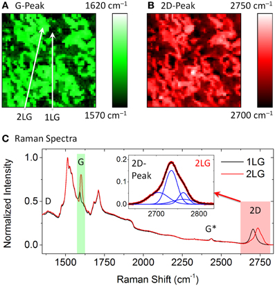
Figure 1. Raman shift map of a 20 × 20 μm2 area showing the variations in the position of (A) G-peak and (B) 2D-peak, where 1LG has a dark and 2LG has a bright contrast. (C) Raman spectra for 1LG and 2LG at the locations indicated in (A). Inset shows the 2D-peak in 2LG fitted with four Lorentzians (blue).
The devices were fabricated using 3-stage standard CMOS technology process. Stage-1 involved defining the wire bonding pads using Electron Beam Lithography (EBL), Oxygen Plasma Etching (OPE) and Electron Beam Physical Vapor Deposition (EBPVD) of Cr/Au (5/100 nm). The OPE step here is crucial for good adhesion of the bonding pad to the substrate. Stage-2 involved defining the metal contact leads using EBL and EBPVD of Cr/Au (5/100 nm) (Blue areas in Figure 2). Note, the OPE step in stage-2 is deliberately absent, thus allowing the Cr/Au to form a direct electrical contact to the graphene. Stage-3 involved using EBL and OPE to define the device (Green areas in Figure 2). Prior to stage-3, large areas around the devices were imaged with Frequency-Modulated (FM-) KPFM [26] to determine the location of 1LG and 2LG (background image in Figure 2). The EBL mask was adapted such that the location of 2LG islands on the Hall bar devices was precisely controlled (as in Figure 2) or avoided entirely, thus forming a uniform 1LG device. A total of 10 devices, with the channel width ranging from 660 to 970 nm, were fabricated using this technique. The SGM measurements were performed on three devices consisting of (#1) uniform 1LG, (#2) uniform 2LG and (#3) non-uniform (i.e., 1–2) number of graphene layers (Table 1).
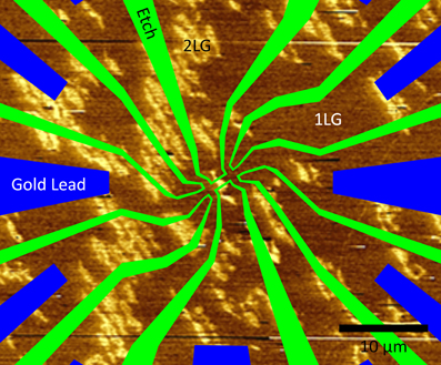
Figure 2. Overlay of the EBL patterning mask (device #3) on FM-KPFM map of the relevant graphene sample. Dark areas are 1LG and light areas are 2LG islands.
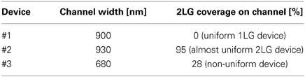
Table 1. Summary of the geometry and 2LG coverage for devices used for SGM measurements.
Transport Measurements
The transport properties of the 10 devices with different 2LG coverage were characterized in ambient air and dark environment using magnetotransport measurement techniques [45]. The carrier density (n) was characterized with the Hall effect by measuring the Hall voltage (VH) response of a current biased (Ibias) device, to a sweeping out-of-plane magnetic fields (B) (Figure 3A). The slope (VH/B) of the resulting linear response was divided by the applied Ibias, characterizing the Hall coefficient (RH = VH/IbiasB). The carrier density was then determined using n = 1/eRH, where e is the electronic charge. The channel resistance (R4 = Vxx/Ibias) was determined using the 4-point technique by measuring the transverse voltage (Vxx) of the current biased device (Figure 3A). The Hall coefficient, channel resistance, channel length (L) and width (W) were used to characterize the carrier mobility (μ = RHL/R4W). The electron carrier density and mobility for the devices are in the range of ne ~2–10 × 1012 cm−2 and μe ~300–2000 cm2V−1s−1, respectively. Prior to the experiments, contact-mode Atomic Force Microscopy (AFM) was used to mechanically clean the devices of resist residues, which are known to affect ne and μe of graphene [5, 17].
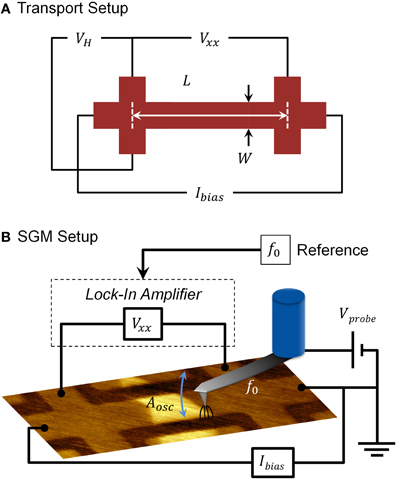
Figure 3. Experimental setups for (A) transport and (B) SGM measurements.
Scanning Gate Microscopy and Point Gate Spectroscopy
SPM measurements were carried out on a Bruker Icon SPM in ambient environment, at controlled temperature of 22°C and relative humidity of ~40%. Bruker SCM-PIT Pt-Ir coated probes with a radius of ~20 nm and a force constant of ~0.8 Nm−1 were used in all experiments. The measurements were performed as a two-pass technique. The first pass involved scanning a single line with tapping mode AFM to determine the surface topography. The second pass (SGM, Figure 3B) involved retracing the surface topography line profile at a set lift height (~20 nm) from the surface. During the SGM pass, a DC voltage was applied to the electrically conductive probe (Vprobe), while the probe was mechanically oscillated at its resonant frequency (f0 ~75 kHz) with an oscillation amplitude of Aosc ~70 nm (peak-peak). The specified lift height of 20 nm dictates the minimum (maximum) probe-sample distance to be 20 (90) nm during the SGM measurements. Also during the second pass, a Stanford Research Systems SR830 Lock-In Amplifier (LIA), referenced to f0, was used to measure the longitudinal voltage (Vxx) of the DC current biased (Ibias) devices. Although Vprobe produces a DC electric field, the device experiences a modulated electric field (i.e., field gradient) due to the mechanical oscillation of the probe at f0 and Aosc. As Vxx is measured with the LIA referenced to f0, the measured device response is only related to the modulated electric field, which locally perturbs the carrier density of the graphene. The signal from the LIA was synchronously fed back into the SPM, recording the device response to the local electric field produced by the probe. This two-pass AFM-SGM technique was performed in an alternating matter to build up a 2-dimensional image of the surface topography and Vxx response of the device.
Point Gate Spectroscopy (PGS) is a measurement technique performed at a single well-defined (x, y) position. The technique involves oscillating the probe at f0 and sweeping Vprobe from −5 to +5 V, while recording Vxx response of the current-biased device with the LIA referenced to f0. PGS allows us to investigate the response of the device to a large range of Vprobe with millivolt resolution without the need to perform hundreds of time consuming SGM scans. PGS also prevents wearing out the metallic coating of the probe, thus leaving it unchanged throughout the duration of the experiment.
Results
Graphene Layer Uniformity
The graphene layer uniformity of devices #1, #2 and #3 (W = 900, 930 and 680 nm, respectively), was determined with topography and surface potential (SP) measurements using FM-KPFM [26], see Table 1. The SP map of device #1 (Figure 4A) shows a single level of contrast on the channel, which signifies 100% uniformity of 1LG. The SP maps of devices #2 and #3 (Figures 4B,C) reveal a double level of contrast on the channel, where the darker and lighter regions are attributed to 1LG and 2LG, respectively. The presence of small 1LG patches on device #2 reduces the uniformity of 2LG on the channel to ~95%, whereas the large 2LG patch at the center of the channel of device #3 corresponds to 2LG coverage of ~28%. The topography map of device #3 clearly shows the SiC etch that forms the device and ~1 μm wide terraces, which are the result of a slight miscut angle (0.11°) of the SiC substrate (Figure 4D). Even though the device spans across a few terraces, the graphene layer is continuous across the terrace edges, as can be seen from the comparison of the SP map and topography image (Figures 4C,D).
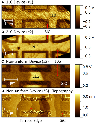
Figure 4. Surface potential maps of devices (A) #1, (B) #2, and (C) #3, with channel widths of 900, 930, and 680 nm, respectively, obtained using FM-KPFM and showing locations of 1LG and 2LG. (D) Topography map of device #3 showing terrace edges and etched SiC.
Effects of Bi-Layer Graphene on Bulk Transport Properties
To understand the transport properties of graphene devices with uniform and non-uniform layer coverage, the bulk carrier density and sheet resistance (Rs) measurements were performed on 10 devices of a similar channel width, i.e., ~660–970 nm, containing 2LG islands of different size and geometry. The carrier density and sheet resistance are plotted in dependence on the percentage of 2LG domains covering the total area of the cross (Figure 5A bottom inset) or channel (Figure 5B inset), respectively. On average, the carrier density measurements conducted in the Hall cross geometry reveal that uniform 1LG exhibits ne ~ 2 × 1012 cm−2 (Figure 5A). However, increasing the percentage of 2LG coverage on the cross area leads to a linear rise of the carrier density, up to ne ~ 8 × 1012 cm−2 for a cross made of ~95% 2LG. Sheet resistance measurements conducted along the channel using the 4-point technique show that uniform 1LG exhibits Rs ~3.2 kΩ, which falls linearly with increasing percentage of 2LG, down to Rs ~0.9 kΩ for channel made up of ~95% 2LG1.
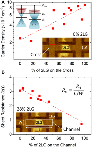
Figure 5. Dependence of (A) carrier density and (B) sheet resistance on the 2LG coverage (in percent) as present on the total area of the cross (red box in (A) bottom inset) and channel (white box in (B) inset), respectively. The dashed lines in main panels are guide for the eye only. The bottom insets are FM-KPFM maps of device #3. The top inset in (A) shows the schematic of linear (1LG) and parabolic (2LG) band structure for n-type graphene with aligned Fermi energies (EF). Evac and ED are the energy levels of vacuum and Dirac point, respectively.
Local Electric Field Effects
SGM was first applied to study the effect of a local electric field on Vxx of a DC current biased device. The Vxx response to the electric field produced by the metallic probe with Vprobe at a lift height of 20 nm is shown in Figures 6A–C, for devices #1, #2, and #3, respectively. Line profiles of ΔR4 = R4 (Vprobe) − R4(0) along the red, green and blue lines indicated in Figures 6A–C for devices #1, #2, and #3, respectively, are shown in Figure 6D.
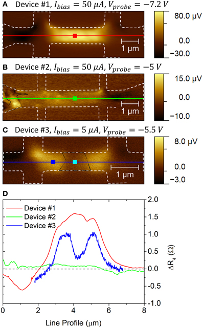
Figure 6. Vxx maps obtained at 20 nm lift height for (A) uniform 1LG device #1, (B) uniform 2LG device #2 and (C) non-uniform device #3 (~28% of 2LG) at the specified Ibias and Vprobe. The white dashed lines in (A–C) marks out the geometrical edge of the device. The areas outlined in black in (B,C) mark out the locations of 1LG and 2LG islands, respectively. (D) Line profiles of ΔR4 along the lines as indicated in (A–C) for devices #1, #2, and #3, respectively. The colored squares in (A–C) are locations for PGS measurements shown in Figure 7.
For device #1, the map and line profile show that probe gating on the channel (denoted by the white box in Figure 5B inset) with Vprobe = −7.2 V increases Vxx and thus ΔR4 (Figures 6A,D, respectively). The maximum response occurs when the probe is located at the center of the channel, owing to the maximum capacitive coupling between the probe and the channel. Modeling of the electric field for such geometry gives a maximum local area capacitance of Cprobe_max ~900 μF/m2 with a spatial decay length of λ ~60 nm [46]. ΔR4 significantly decreases when the probe is gating on the left/right side of the channel. Similarly, for device #2, gating on the channel also increases ΔR4, however, with a much more flat response along the channel (Figure 6B). Furthermore, the maximal magnitude of the response for device #2 is ~20 times lower than device #1. It is noteworthy that the increased signal in the left part of the channel (device #2) is attributed to the presence of a small 1LG domain indicated by the area outlined in black (Figure 6B). For device #3, ΔR4 increases (decreases) when the probe is gating inside (outside) the 1LG part of the channel (Figure 6C), i.e., in a similar fashion to device #1. However, the significant decrease of ΔR4 (i.e., ~3 times with respect to 1LG) is seen in device #3, when the probe gates on the 2LG island (outlined in black) located at the center of the channel, indicates suppression of the electric field gating.
To compare the local electric field gating effects for the three studied devices, PGS measurements were performed by sweeping Vprobe from −5 to +5 V and recording the Vxx response. These measurements are shown as ΔR4 in Figure 7. For all the PGS measurements, applying a negative (positive) Vprobe increases (decreases) ΔR4.
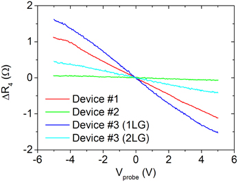
Figure 7. PGS measurements showing ΔR4 obtained at the locations indicated by the colored squares in Figures 6A–C for devices #1, #2, and #3, respectively.
Discussion
The 2LG system cannot be simply regarded as two single-layers stacked on top of each other as the relevant 2D-peak from the Raman spectrum can be accurately fitted by four Lorentzians, which is a good indication of AB or Bernal stacking (Figure 1C inset). In this case, the top and bottom layers are arranged such that the carbon atoms in the top layer are in the center of the bottom layer hexagon. This type of stacking of 2LG results in strong interlayer coupling, which causes the linear π-band to split into two parabolic branches near the K Dirac point. Although the band structures for 1LG and 2LG are unique, the Fermi energy (EF) is still aligned due to the electronic connection between the two layers. Therefore, increase in the surface potential observed with FM-KPFM is the result of a smaller work function for 2LG. As EF for 1LG and 2LG are aligned, the position of the Dirac point (ED) is shifted down for 2LG (Figure 5A top inset). This increases the density of states (DOS) in the 2LG system, which is observed as an increase in the carrier density with bulk transport measurements (Figure 5A).
Applying a negative Vprobe to device #1 (1LG) locally depletes the electrons, increasing the total resistance of the channel, which is observed as an increase in Vxx in SGM measurements (Figure 6A). The gating induced change of ΔR4 increases as the effective gating area (Aeff, ∅ ~1 μm) spreads over the channel, while the probe moves left to right (see Movie 1 in online supplementary information). When Aeff is totally encompassed within the channel, ΔR4 saturates, with maximum gating efficiency occurring when probe is located at the center of the channel (Figure 8A). The large effective gating area is the result of charge diffusing from the probe to graphene and the area is strongly depends on Vprobe [23, 47–49]. We should stress that the Aeff specified here provides only an empirical measure of the effect, rather than its accurate estimate, for which thorough theoretical calculations are required. Despite the fact that electric field is highly localized to the probe apex of ∅ ~40 nm, the effected gating area is significantly larger, affecting the distribution of charges over a large area of the channel (Figure 8B). However, it is also apparent that, when the probe is gating outside of the device geometrical edge (dashed white lines in Figure 8A) where there is no graphene, the localized electric field has no real effect on Vxx. On device #2, the gating efficiency is essentially uniform with no clear maximum across the length of the channel (Figures 6B,D). Furthermore, the gating effect is ~20 times lower than that on device #1 at identical experimental parameters, indicating the 2LG behaves similarly to a conventional metal, screening the electric field. On device #3, the 2LG island at the center clearly decreases the gating effect, however not to the same extent as demonstrated in uniform 2LG device #2.
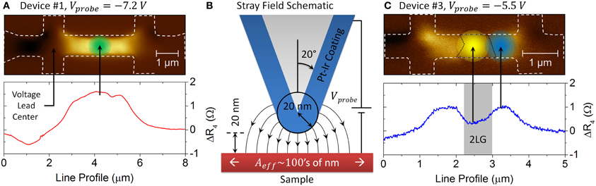
Figure 8. Schematic representation of the effective area (Aeff) affected by the local electrical gate: Vxx maps of (A) device #1 and (C) device #3 showing the change of the resistance of the circled areas that is influenced by a local electrical top gate. The diameters of the circles are empirically estimated as ∅ ~1 μm (green) and ∅ ~0.9 μm (blue/yellow) having taken into account the differences in Vprobe and the channel width. (B) Schematic of the electrostatic field emanating from the probe apex of ∅ ~40 nm.
Further, we compare the screening efficiency of the local gating as measured at the geometrical center of each device for different layer thicknesses and configurations. PGS measurements show that the gating Vprobe ~ −5 V at the center of the channel leads to the absolute change of the resistance ΔR4 ~ 1.1 Ω for device #1 (Figure 7). Assuming the identical screening mechanism and considering the Rs for device #2 is 4.6 times lower than device #1 (Table 2), the expected response at Vprobe ~ −5 V is ΔR4 ~0.24 Ω. However, the experimental value for device #2 is ~20 times lower, being only ΔR4 ~0.06 Ω. The clear reduction in the gating efficiency is indicative of an additional screening component in the uniform 2LG device. Comparing the ratio of ΔR4/Rs for device #1 (4.8 × 10⁻⁴) and #2 (1.2 × 10⁻⁴), the relative gating efficiency decreases by ~75% for the uniform 2LG device #2. It is noteworthy that the relative change of the resistance induced by the local gate is very small (i.e. fraction of a percent) on the background of large Rs values of the devices. Although Vprobe produces a relatively large electric field, the mechanical oscillation at f0 and Aosc ~70 nm weakly modulates this field. As Vxx is measured with the LIA referenced to f0, the measured signal is only related to the weak modulation of the electric field, leading to a considerably smaller response of ΔR4 compared to R4.
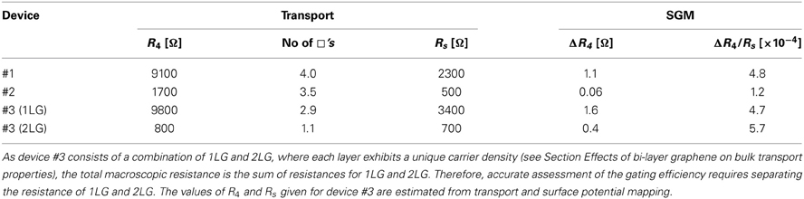
Table 2. A summary of the DC transport and PGS measurements for devices #1, #2 and #3, where R4 is the 4-point resistance; □ is the ratio of channel length/width (L/W), Rs is the sheet resistance, ΔR4 = R4(Vprobe) – R4(0) is the absolute change of the R4 under the effect of the local gate; ΔR4/Rs is a relative change of the R4 under the effect of the local gate.
On the non-uniform device #3, the gating effect at Vprobe ~ −5 V on 1LG and 2LG parts yielded a response of ΔR4 ~ 1.6 and 0.4 Ω, respectively (Figure 7 and Table 2). It is necessary to stress that recording ΔR4 is a measure of the total channel length. In the case of device #3, the channel is a mixture of 1LG and 2LG with different values of Rs, owing to the ~4 times larger carrier density for 2LG (Figure 5A). Thus, accurate assessment of the gating efficiency requires separating the resistance of 1LG and 2LG. Rs can be precisely determined as 3.4 and 0.7 kΩ (Table 2) for 1LG and 2LG, respectively, by calculating the area of the 2LG island from the FM-KPFM map (Figure 4C). For device #3, ΔR4/Rs = 4.7 × 10⁻⁴ and 5.7 × 10⁻⁴ for gating on 1LG and 2LG, respectively (Table 2). However, as the local electric field influences the electronic properties across a relatively large area of the channel (i.e., comparable to the area of 2LG island), it is not possible to accurately assess the gating efficiency from ΔR4/Rs. Here, gating on 1LG part of the device also contains the contribution from gating on 2LG (see Movie 2 in online supplementary information), as indicated by the area circled in blue (∅ ~0.9 μm) in Figure 8C. Similarly, gating on 2LG (yellow circled area) contains contributions from 1LG. While differences in the gating effect on 1LG and 2LG are averaged out in conventional macroscopic measurements on top or back-gated non-uniform graphene devices, such as field-effect transistors, SGM and PGS results show a direct effect of 2LG islands on transport properties.
It is well-known that bilayer graphene can be either Bernal stacked (interacting layers) or rotationally faulted (“twisted bilayer”), in later case the individual layers are generally considered as non-interacting, see e.g., [50]. It has been shown that bilayer graphene grown on the Si-side of SiC substrates (i.e., similar to the material considered here) is Bernal stacked [51, 52], so the system possesses a tunable energy band gap.
An understanding of the charge screening is essential for majority of the proposed graphene applications. The screening determines how the carrier concentration depends on the number of graphene layers and the gate voltage. It also determines the effectiveness with which substrate affects the electronic properties of graphene [53]. The screening efficiency is also largely influenced by the interlayer interaction. In general, the observed effect of screening (suppression) of the local electric field by 2LG can be qualitatively explained by electron-electron (Coulomb) interactions and tunneling effects leading to new phenomena, which are not present in the individual layers, e.g., interlayer charge transfer and the screening of external potentials.
This effect has recently inspired a number of very interesting experimental and theoretical studies. For example, it was theoretically demonstrated that in the case of non-interacting graphene layers, the screening is highly nonlinear due to the specific electronic structure of graphene with vanishing DOS at the Fermi level [53]. In the out-of-plane geometry, the decay is not simply exponential: the larger the external bias, the stronger the screening leading to the shorter screening length. In the same work it was also calculated that the characteristic screening length may vary about an order of magnitude, i.e., from several times the graphene interlayer spacing down to a fraction of a layer. The reduction of screening in deeper layers of multi-layered graphene has been explained in terms of moving the Fermi level closer to the Dirac point, hence reducing the DOS at the Fermi level. The screening may change considerably when the system is doped due to minority-carrier screening. For moderate charge densities, i.e., comparable to our work ~1012 cm−2, thermal effects might be significant even at the room temperature, as states around the Fermi level become available due to the thermal broadening of the charge distribution [53].
It has also been shown that such important electrostatic properties of graphene as capacitance, charge screening, and energy storage capability can be significantly affected by external electric fields. For example, it has been calculated that both the out-of-plane and the in-plane dielectric constants (κ) of graphene depend on the value of applied field and number of layers, i.e., being nearly constant (κ ~3 and ~1.8, respectively) at low fields but increasing up to κ ~13 and ~15 at higher fields [54]. The authors showed that application of external perpendicular field (Eext⊥) generates an interlayer charge-transfer, which partially compensates the external field, producing the value of the effective field (Eeff⊥), Eeff⊥ < Eext⊥. For example, for the range of fields considered here, Eext⊥ ≅ 2.5 × 10³ kV/cm, ~50% reduction of the external field in between the layers of 2LG can be expected. If to consider a thicker sample, the enhancement of κ with the number of layers was directly correlated to the reduction of Eeff⊥ in the innermost regions [54]. The effect was explained by the nonlinear nature of the screening in multilayer graphene.
The dielectric properties of the substrate can also affect the local gating. For example, substrate surface phonons uniformly affect the electronic properties of graphene via electrostatic coupling of the carriers with the long-range polarization field created at the graphene-substrate interface [49]. However, the application of a local gate will lead to local inhomogeneity in the electron scattering rate. This effect is more pronounced for graphene on substrates such as SiC (as in the present work) with lower dielectric constant (κSiC = 9.7), whereas the local gate is efficiently screened in graphene on substrates such as STO with very high dielectric constants (κSTO = 330) [49].
The effect of electrical screening can also be studied by combination of external perpendicular magnetic and electrical fields. By analyzing the gate dependence of the Landau level crossings in twisted (non-interacting) graphene, the finite interlayer screening and capacitance between the atomically spaced layers have been characterized [55]. By varying the gate voltages, the authors observed interlayer Landau level crossings, which allowed quantifying both the charge transfer and finite screening effects between the layers. The partial screening of the external electrical field was attributed to graphene's small DOS and close spacing between the layers.
Differences in the electronic properties of Bernal stacked and rotationally faulted (twisted) bilayer CVD grown graphene have been experimentally studied [50] and attributed to the differences in their band structure (i.e., non-interacting single layers in the case of the twisted graphene) leading to the effective screening of the electrical potential.
It should be taken into account that SPM techniques are prone to scanning and probe-induced artifacts, requiring meticulous attention during the data acquisition process [56]. For example, the probe mechanical oscillation amplitude (Aosc) strongly affects the electric field gradient and device response, which could be misinterpreted as a real property of the device. In the present study, Aosc was monitored throughout the experiment to ensure Vprobe was kept below the threshold for strong probe-sample interaction. We find that these effects can typically play a significant role for Vprobe > ±5 V. Additionally, the probe mechanically contacting the surface can lead to electrical shorting, resulting in a substantial amount of current flowing from the probe to sample [57], further affecting the device response. Our in situ measurements of the leakage current showed that, whether such effect is controllably induced, it can be a few microamperes large, i.e., comparable with Ibias used throughout the experiments. The electrical breakdown of air can also be a significant factor affecting the leakage current [57]. The latter was also considered at Vprobe up to ±10 V, where a maximum leakage current of sub-picoamperes was observed, thus indicating the air resistance is ~70 TΩ. After carefully considering all the above effects, we can be confident that they are not applicable in our case.
While we aimed at experimental demonstration of screening of external electrical potential, detailed understanding of screening effects in bilayer epitaxial graphene requires complex theoretical studies and is outside of the scope of this paper.
Conclusion
In summary, we investigated the effects of electrical screening in uniform and non-uniform 1-2LG graphene devices using a combination of macroscopic DC transport measurement and the local SGM technique. The size and location of 2LG islands were mapped using FM-KPFM and correlated with DC transport measurements to show that the channel resistance linearly decreases with the area of 2LG islands, owing to a 4 times larger carrier density in 2LG. In addition, local electric field effects were investigated in uniform and non-uniform devices by SGM. In uniform 1LG and 2LG devices, applying a negative (positive) gate voltage increased (decreased) the resistance of the channel, which can be explained by electrostatic considerations. The gating effect was ~20 times weaker in 2LG, which indicates screening (suppression) of the local electric field by ~75%. A similar screening effect was observed in a non-uniform device containing a 2LG island at the center of the channel. However, in this case, the efficiency of the electric field screening by 2LG was significantly lower. Although the electric field is highly localized, the carriers in the graphene are significantly redistributed, as described by Aeff. This area is comparable to the size of the 2LG patch, therefore gating on the 2LG patch leads to contributions from 1LG part of the device, which results in an additional averaging of the gating effect. These results experimentally demonstrate the local electric field screening behavior of 2LG, which is not addressable by standard transport measurements alone.
In majority of the applications, presence of 2LG can be beneficial at lowering the device resistance. However, for example in magnetic field sensing applications, the presence of 2LG on the sensor area of Hall devices can significantly lower the sensitivity. In gas sensing applications, inhomogeneity of graphene coverage may lead to preferable absorption of analyte molecules on the specific side and compromise interpretation of the electrical readout. Thus, careful considerations of the device layout and thickness are required for each envisaged application.
Conflict of Interest Statement
The authors declare that the research was conducted in the absence of any commercial or financial relationships that could be construed as a potential conflict of interest.
Acknowledgments
We are very grateful to John Gallop, Alexander Tzalenchuk and Jonathan Fletcher for useful discussions and Héctor Corte-León for help with MATLAB scripts for Raman spectra analysis.
Funding
NMS under the IRD Graphene Project (NPL) and EMRP Project “GraphOhm.”
Supplementary Material
The Supplementary Material for this article can be found online at: http://www.frontiersin.org/journal/10.3389/fphy.2014.00003/abstract
Footnotes
1. ^Note: Rs values specified in section Effects of bi-layer graphene on bulk transport properties and Figure 5 are somewhat different from those specified in section Local electric field effects as day-to-day changes in the ambient conditions affect the doping and thus, the carrier density of the graphene.
References
1. Dimitrakopoulos C, Lin YM, Grill A, Farmer DB, Freitag M, Sun Y, et al. Wafer-scale epitaxial graphene growth on the Si-face of hexagonal SiC (0001) for high frequency transistors. J Vac Sci Technol B Microelectron Nanom Struct. (2010) 28:985–92. doi: 10.1116/1.3480961
2. Lin YM, Dimitrakopoulos C, Jenkins KA, Farmer DB, Chiu HY, Grill, A, et al. 100-GHz transistors from wafer-scale epitaxial graphene. Science (2010) 327, 662. doi: 10.1126/science.1184289
3. Panchal V, Burnett TL, Pearce R, Cedergren K, Yakimova R, Tzalenchuk A, et al. Surface potential variations in epitaxial graphene devices investigated by Electrostatic Force Spectroscopy. 12th IEEE Conf Nanotechnol. (2012) 1–5. doi: 10.1109/NANO.2012.6322049
4. Yakimova R, Virojanadara C, Gogova D, Syväjärvi M, Siche D, Larsson, K, et al. Analysis of the formation conditions for large area epitaxial graphene on SiC substrates. Mater Sci Forum (2010) 645–648:565–568. doi: 10.4028/www.scientific.net/MSF.645-648.565
5. Kazakova O, Panchal, V, Burnett, T. Epitaxial graphene and graphene–based devices studied by electrical scanning probe microscopy. Crystals (2013) 3:191–233. doi: 10.3390/cryst3010191
6. Yu YJ, Zhao Y, Ryu S, Brus LE, Kim KS, Kim P. Tuning the graphene work function by electric field effect. Nano Lett. (2009) 9:3430–4. doi: 10.1021/nl901572a
7. Filleter T, Emtsev KV, Seyller T, Bennewitz, R. Local work function measurements of epitaxial graphene. Appl Phys Lett (2008) 93: 133117. doi: 10.1063/1.2993341
8. Wang T, Guo Q, Liu, Y, Sheng K. A comparative investigation of an AB- and AA-stacked bilayer graphene sheet under an applied electric field: a density functional theory study. Chinese Phys B (2012) 21: 067301. doi: 10.1088/1674-1056/21/6/067301
9. Chuang YC, Wu JY, Lin MF. Electric field dependence of excitation spectra in AB-stacked bilayer graphene. Sci Rep. (2013) 3: 1368. doi: 10.1038/srep01368
10. Childres I, Jalilian R, Foxe M, Chernyshov A, Rohkinson L, Jovanovic, I, et al. “Effect of energetic electron irradiation on graphene,” in AIP Conference Proceedings (AMER INST PHYSICS) (Crete), (2009) 140–4.
11. Childres I, Jauregui LA, Foxe M, Tian J, Jalilian R, Jovanovic I, et al. Effect of electron-beam irradiation on graphene field effect devices. Appl Phys Lett. (2010) 97: 173109. doi: 10.1063/1.3502610
12. Jalilian R, Jauregui LA, Lopez G, Tian J, Roecker C, Yazdanpanah MM, et al. Scanning gate microscopy on graphene: charge inhomogeneity and extrinsic doping. Nanotechnology (2011) 22: 295705. doi: 10.1088/0957-4484/22/29/295705
13. Kim EA, Castro Neto AH. Graphene as an electronic membrane. Eur Lett. (2008) 84: 57007. doi: 10.1209/0295-5075/84/57007
14. Chen JH, Jang C, Adam S, Fuhrer MS, Williams ED, Ishigami M. Charged-impurity scattering in graphene. Nat Phys. (2008) 4:377–81. doi: 10.1038/nphys935
15. Zhang Y, Brar VW, Girit C, Zettl A, Crommie MF. Origin of spatial charge inhomogeneity in graphene. Nat Phys. (2009) 5:722–6. doi: 10.1038/nphys1365
16. Wehling TO, Novoselov KS, Morozov SV, Vdovin EE, Katsnelson MI, Geim AK, et al. Molecular doping of graphene. Nano Lett. (2008) 8:173–7. doi: 10.1021/nl072364w
17. Lara-Avila S, Moth-Poulsen K, Yakimova R, Bjørnholm T, Fal'ko V, Tzalenchuk, A, et al. Non-volatile photochemical gating of an epitaxial graphene/polymer heterostructure. Adv Mat. (2011) 23:878–82. doi: 10.1002/adma.201003993
18. Connolly MR, Chiou KL, Smith CG, Anderson D, Jones GAC, Lombardo A, et al. Scanning gate microscopy of current-annealed single layer graphene. Appl Phys Lett. (2010) 96: 113501. doi: 10.1063/1.3327829
19. Giovannetti G, Khomyakov P, Brocks G, Karpan, V, van den Brink, J, Kelly P. Doping graphene with metal contacts. Phys Rev Lett. (2008) 101:4–7. doi: 10.1103/PhysRevLett.101.026803
20. Golizadeh-Mojarad R, Datta S. Effect of contact induced states on minimum conductivity in graphene. Phys Rev B (2009) 79: 085410. doi: 10.1103/PhysRevB.79.085410
21. Martin J, Akerman N, Ulbricht G, Lohmann T, Smet JH, von Klitzing K, et al. Observation of electron–hole puddles in graphene using a scanning single-electron transistor. Nat Phys. (2007) 4:144–8. doi: 10.1038/nphys781
22. Deshpande A, Bao W, Miao F, Lau, C, LeRoy B. Spatially resolved spectroscopy of monolayer graphene on SiO2. Phys Rev B (2009) 79: 205411. doi: 10.1103/PhysRevB.79.205411
23. Giannazzo F, Fisichella G, Lo Nigro R, Fiorenza P, Di Franco S, Marino A, et al. Scanning probe microscopy investigation of the mechanisms limiting electronic transport in substrate-supported graphene. Phys Status Sol. (2013) 10:1188–92. doi: 10.1002/pssc.201200974
24. Lee EJH, Balasubramanian K, Weitz RT, Burghard M, Kern K. Contact and edge effects in graphene devices. Nat Nanotechnol. (2008) 3:486–90. doi: 10.1038/nnano.2008.172
25. Burnett T, Yakimova R, Kazakova O. Mapping of local electrical properties in epitaxial graphene using electrostatic force microscopy. Nano Lett. (2011) 11:2324–8. doi: 10.1021/nl200581g
26. Panchal V, Pearce R, Yakimova R, Tzalenchuk A, Kazakova O. Standardization of surface potential measurements of graphene domains. Sci Rep. (2013) 3: 2597. doi: 10.1038/srep02597
27. Eriksson MA, Beck RG, Topinka M, Katine JA, Westervelt RM, Campman KL, et al. Cryogenic scanning probe characterization of semiconductor nanostructures. Appl Phys Lett. (1996) 69: 671. doi: 10.1063/1.117801
28. Eriksson MA, Beck RG, Topinka MA, Katine JA, Westervelt RM, Campman KL, et al. Effect of a charged scanned probe microscope tip on a subsurface electron gas. Superlat Microstruct. (1996) 20:435–40. doi: 10.1006/spmi.1996.0100
29. Topinka MA, LeRoy BJ, Westervelt RM, Shaw SE, Fleischmann R, Heller EJ, et al. Coherent branched flow in a two-dimensional electron gas. Nature (2001) 410:183–6. doi: 10.1038/35065553
30. Aoki N, da Cunha C, Akis R, Ferry D, Ochiai Y. Imaging of integer quantum Hall edge state in a quantum point contact via scanning gate microscopy. Phys Rev B (2005) 72: 155327. doi: 10.1103/PhysRevB.72.155327
31. Yang C, Zhong, Z, Lieber CM. Encoding electronic properties by synthesis of axial modulation-doped silicon nanowires. Science (2005) 310:1304–7. doi: 10.1126/science.1118798
32. Bachtold A, Fuhrer M, Plyasunov S, Forero M, Anderson E, Zettl A, et al. Scanned probe microscopy of electronic transport in carbon nanotubes. Phys Rev Lett. (2000) 84:6082–5. doi: 10.1103/PhysRevLett.84.6082
33. Tans S, Dekker C. Potential modulations along carbon nanotubes. Nature (2000) 404:834–5. doi: 10.1038/35009026
34. Bockrath M, Liang W, Bozovic D, Hafner JH, Lieber CM, Tinkham M, et al. Resonant electron scattering by defects in single-walled carbon nanotubes. Science (2001) 291:283–5. doi: 10.1126/science.291.5502.283
35. Freitag M, Johnson A, Kalinin S, Bonnell, D. Role of single defects in electronic transport through carbon nanotube field-effect transistors. Phys Rev Lett (2002) 89: 216801. doi: 10.1103/PhysRevLett.89.216801
36. Pascher N, Bischoff D, Ihn T, Ensslin K. Scanning gate microscopy on a graphene nanoribbon. Appl Phys Lett. (2012) 101: 063101. doi: 10.1063/1.4742862
37. Garcia AGF, König M, Goldhaber-Gordon D, Todd K. Scanning gate microscopy of localized states in wide graphene constrictions. Phys Rev B (2013) 87: 085446. doi: 10.1103/PhysRevB.87.085446
38. Connolly MR, Herbschleb ED, Puddy RK, Roy M, Anderson D, Jones GAC, et al. Reading and writing charge on graphene devices. Appl Phys Lett. (2012) 101: 023505. doi: 10.1063/1.4732802
39. Connolly MR, Puddy RK, Logoteta D, Marconcini P, Roy M, Griffiths JP, et al. Unraveling quantum Hall breakdown in bilayer graphene with scanning gate microscopy. Nano Lett. (2012) 12:5448–54. doi: 10.1021/nl3015395
40. Schnez S, Güttinger J, Huefner M, Stampfer C, Ensslin, K, Ihn, T. Imaging localized states in graphene nanostructures. Phys Rev B (2010) 82:1–5. doi: 10.1103/PhysRevB.82.165445
41. Prakash G, Bolen ML, Colby R, Stach EA, Capano MA, Reifenberger R. Nanomanipulation of ridges in few-layer epitaxial graphene grown on the carbon face of 4H-SiC. New J Phys. (2010) 12: 125009. doi: 10.1088/1367-2630/12/12/125009
42. Yazdi GR, Vasiliauskas R, Iakimov T, Zakharov A, Syväjärvi M, Yakimova R. Growth of large area monolayer graphene on 3C-SiC and a comparison with other SiC polytypes. Carbon N.Y (2013) 57:477–84. doi: 10.1016/j.carbon.2013.02.022
43. Lee DS, Riedl C, Krauss B, von Klitzing K, Starke U, Smet JH. Raman spectra of epitaxial graphene on SiC and of epitaxial graphene transferred to SiO2. Nano Lett. (2008) 8:4320–5. doi: 10.1021/nl802156w
44. Röhrl J, Hundhausen M, Emtsev KV, Seyller T, Graupner R, Ley L. Raman spectra of epitaxial graphene on SiC(0001). Appl Phys Lett. (2008) 92: 201918. doi: 10.1063/1.2929746
45. Panchal V, Cedergren K, Yakimova R, Tzalenchuk A, Kubatkin, S, Kazakova O. Small epitaxial graphene devices for magnetosensing applications. J Appl Phys. (2012) 111: 07E509. doi: 10.1063/1.3677769
46. Rajkumar RK, Asenjo A, Panchal V, Manzin A, Iglesias-Freire O, Kazakova O. Magnetic scanning gate microscopy of graphene hall devices. J Appl Phys. (2013).
47. Giannazzo F, Sonde S, Raineri, V, Rimini, E. Screening length and quantum capacitance in graphene by scanning probe microscopy. Nano Lett. (2009) 9:23–9. doi: 10.1021/nl801823n
48. Giannazzo F, Sonde S, Raineri, V, Rimini E. Irradiation damage in graphene on SiO[sub 2] probed by local mobility measurements. Appl Phys Lett. (2009) 95: 263109. doi: 10.1063/1.3280860
49. Giannazzo F, Sonde S, Lo Nigro R, Rimini E, Raineri, V. Mapping the density of scattering centers limiting the electron mean free path in graphene. Nano Lett. (2011) 11:4612–8. doi: 10.1021/nl2020922
50. Fallahazad B, Hao Y, Lee K, Kim S, Ruoff RS, Tutuc E. Quantum hall effect in bernal stacked and twisted bilayer graphene grown on Cu by chemical vapor deposition. Phys Rev B (2012) 85: 201408. doi: 10.1103/PhysRevB.85.201408
51. Riedl C, Coletti C, Iwasaki T, Zakharov AA, Starke U. Quasi-free-standing epitaxial graphene on SiC obtained by hydrogen intercalation. Phys Rev Lett. (2009) 103: 246804. doi: 10.1103/PhysRevLett.103.246804
52. Lee K, Kim S, Points MS, Beechem TE, Ohta T, Tutuc E. Magnetotransport properties of quasi-free-standing epitaxial graphene bilayer on SiC: evidence for Bernal stacking. Nano Lett. (2011) 11:3624–8. doi: 10.1021/nl201430a
53. Kuroda MA, Tersoff J, Martyna GJ. Nonlinear screening in multilayer graphene systems. Phys Rev Lett. (2011) 106: 116804. doi: 10.1103/PhysRevLett.106.116804
54. Santos EJG, Kaxiras E. Electric-field dependence of the effective dielectric constant in graphene. Nano Lett. (2013) 13:898–902. doi: 10.1021/nl303611v
55. Sanchez-Yamagishi JD, Taychatanapat T, Watanabe K, Taniguchi T, Yacoby A, Jarillo-Herrero, P. Quantum hall effect, screening, and layer-polarized insulating states in twisted bilayer graphene. Phys Rev Lett. (2012) 108: 076601. doi: 10.1103/PhysRevLett.108.076601
56. Sellier H, Hackens B, Pala MG, Martins F, Baltazar S, Wallart, X, et al. On the imaging of electron transport in semiconductor quantum structures by scanning-gate microscopy: successes and limitations. Semicond Sci Technol. (2011) 26: 064008. doi: 10.1088/0268-1242/26/6/064008
Keywords: epitaxial graphene, scanning gate microscopy, single-layer graphene, double-layer graphene, electrical gating
Citation: Panchal V, Giusca CE, Lartsev A, Yakimova R and Kazakova O (2014) Local electric field screening in bi-layer graphene devices. Front. Physics 2:3. doi: 10.3389/fphy.2014.00003
Received: 15 November 2013; Paper pending published: 16 December 2013;
Accepted: 10 January 2014; Published online: 03 February 2014.
Edited by:
Peter A. Dowben, University of Nebraska, USAReviewed by:
Mads Brandbyge, Technical University of Denmark, DenmarkIvar Martin, Argonne National Laboratory, USA
Hae Kyung Jeong, Daegu University, Korea (South)
Copyright © 2014 Panchal, Giusca, Lartsev, Yakimova and Kazakova. This is an open-access article distributed under the terms of the Creative Commons Attribution License (CC BY). The use, distribution or reproduction in other forums is permitted, provided the original author(s) or licensor are credited and that the original publication in this journal is cited, in accordance with accepted academic practice. No use, distribution or reproduction is permitted which does not comply with these terms.
*Correspondence: Olga Kazakova, National Physical Laboratory, Quantum Detection, Hampton Road, Teddington TW11 0LW, London, UK e-mail: olga.kazakova@npl.co.uk