Theoretical and experimental investigation of low-volgage and low-loss 25-Gbps Si photonic crystal slow light Mach–Zehnder modulators with interleaved p/n junction
 Yosuke Terada
 Hiroyuki Ito
  Toshihiko Baba
- Department of Electrical and Computer Engineering, Yokohama National University, Yokohama, Japan
In this study, we investigated the performance of Si lattice-shifted photonic crystal waveguide (LSPCW) Mach–Zehnder modulators theoretically and experimentally. The LSPCW increases the phase shift in modulator to 2.3–2.5 times higher, which allows for size reduction and high performance. On-chip passive loss was reduced to less than 5 dB by optimizing each component. We obtained 25 Gbps clear open eye and 3 dB extinction ratio at a drive voltage of 1.5–1.75 V for 200 μm phase shifter with linear p/n junction when we added a modulation loss of 7 dB. This modulation loss was reduced to 0.8 dB, maintaining other performance, by employing interleaved p/n junction and optimizing doping concentrations.
Introduction
Si photonics, which can produce highly integrated photonic circuits using CMOS-compatible process, has been developed extensively toward optical interconnects [1]. Since external light sources are used in current Si photonics, Si modulators based on carrier plasma dispersion (CPD) [2–20], electro-absorption [21, 22], or so are necessary. The CPD in p/n diode structures is practically used in commercial modulators for optical interconnects because of the easy fabrication of the p/n junction and operation over the wide range of wavelength and temperature, which is crucial in optical interconnects. CPD is generated by carrier injection or depletion. The carrier injection gives a larger refractive index change, and its 3-dB cutoff frequency is ~1 GHz or smaller [2] and preemphasized signals are necessary for higher-speed operation [3–5]. Therefore, the carrier depletion that can respond at higher speeds is often employed although the index change is smaller [6–19]. Using resonance effects such as that in microrings is one of the methods that compensate the small index change, but its narrow band hampers to use over the wide range of temperature [4, 6, 7]. On the other hand, Mach–Zehnder (MZ) interferometer modulators have broad band, allowing wide temperature range operation [2, 3, 5, 8–19]. However, their device size is usually of the millimeter-order [7–10, 12–14] and drive voltage is higher than several volts [9–19], which cannot meet the requirements for optical interconnects. To solve this constraint, we have studied slow light with a low group velocity vg [22–24]. Slow light accelerates the efficiency of MZ modulators in proportion to the group index ng = c/υg, where c is the light velocity in vacuum. Silica-cladded Si photonic crystal waveguide produces slow light with a typical ng ~ 20 [16] and can be fabricated easily by CMOS-compatible process [23]. We have proposed and demonstrated Si MZ modulators incorporating this waveguide as phase shifters. First, 10 Gbps operation was observed at carrier injection [5, 15] and carrier depletion [15] in 200-μm-long devices. The preliminary operation at 25–40 Gbps was also obtained in sub-100-μm devices [16]. The operation over the wide range of wavelength (Δλ = 16.9 nm) and temperature (ΔT = 105 K) is confirmed by employing low-dispersion slow light in lattice-shifted photonic crystal waveguide (LSPCW) [17].
In this paper, we discuss the balancing of various performance parameters of the Si LSPCW MZ modulator and improvement of p/n junction, which has not been studied so far for this modulator. In Section Requirements, we generally discuss the requirements for Si MZ modulators and interrelation between performance parameters. In Section Calculations, we explain the detailed structure of the modulator in this study. We quantify slow light enhancement by calculating the CPD-induced index change and phase shift of light, and show a guideline for optimization. We also calculate the electrical resistance and junction capacitance, giving the RC time constant, and discuss how it is related with other performance. In Section Fabrication and measurement, we present the fabrication and measurement results, and demonstrate 10–25 Gbps operations in 90–200 μm devices and low-loss operation by the improved p/n junction and doping concentrations.
Requirements
In general, the normalized output intensity I [dB] of MZ modulators is given for the optical phase ϕ by
and is depicted by the solid line in Figure 1. Here the intensity is normalized by that at ϕ = 0, which actually gives the on-chip passive loss PL without modulation. Setting phase operating point ϕ1 and adding the phase shift Δϕ, output light is modulated with the extinction ratio ER, while the modulation loss ML is added according to ϕ1. ER and ML are expressed as follows:
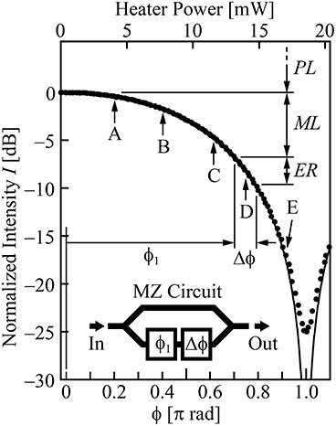
Figure 1. Intensity response (solid line) and measured ones (closed circles) as a function of the phase shift of the MZ modulator and corresponding heater power in phase tuner. The intensity is normalized by that at ϕ1 = 0.
From these equations, we obtain
As ϕ approaches to π, |dI/dϕ| = 10 sin ϕ/(1 + cosϕ) increases, and a large ER is obtained even with small Δϕ. However, the ML increases simultaneously, resulting in low S/N. To meet the requirements of optical interconnects, sufficient ER must be obtained with suppressing the total loss PL + ML. One target value acceptable may be PL + ML < 10 dB, but PL + ML ≤ 5 dB will be demanded finally for loss penalty. In view of the operating voltage of high-speed CMOS driver circuits, the drive voltage of the modulator Vpp should be 1.5 V or lower. The ER of 3 dB or higher is necessary for discriminating digital data. In addition, the data bitrate BR ≥ 25 Gbps achieving a 100 Gbps throughput by preparing four traffic channels, phase shifter length L < 1 mm fitting into a small footprint of optical transceivers and optical interposers, and wavelength range Δλ > 10 nm equivalent to the temperature range ΔT > 100 K and so on will be expected.
Table 1 compares the performance (except for Δλ and ΔT) of Si MZ modulators based on rib waveguides and LSPCW [8–14, 17]. Rib waveguide modulators satisfy the requirements for BR and ER, and not for L, PL, ML, and/or Vpp. The previous performance of LSPCW modulators is similar, except for L. In both modulators, larger Δϕ is necessary for satisfying all the requirements. It is obtainable by increasing ng, L, and Vpp. Here, Vpp must rather be reduced since Vpp in previous studies are too high. The typical value of ng is ~20 (22 is measured in this study, as shown in Section Fabrication and measurement) in the third-row-shifted LSPCW [16]. Although we can increase this value by modifying the structure, Δλ will be narrowed due to the ngΔλ product constraint of slow light and the waveguide loss will be increased by larger ng. We may increase L of the LSPCW since it is already much smaller than the requirement, but it will also increase the waveguide loss. Therefore, we fix these parameters in this paper. Other methods considered for larger Δϕ are employing interleaved p/n junction [7, 10, 18, 19, 25] and increasing doping concentration. The former increases the overlap between the depletion layer and waveguide mode. The latter is expected to increase the quantity of the index change within the limits that the free carrier absorption does not affect severely [26].
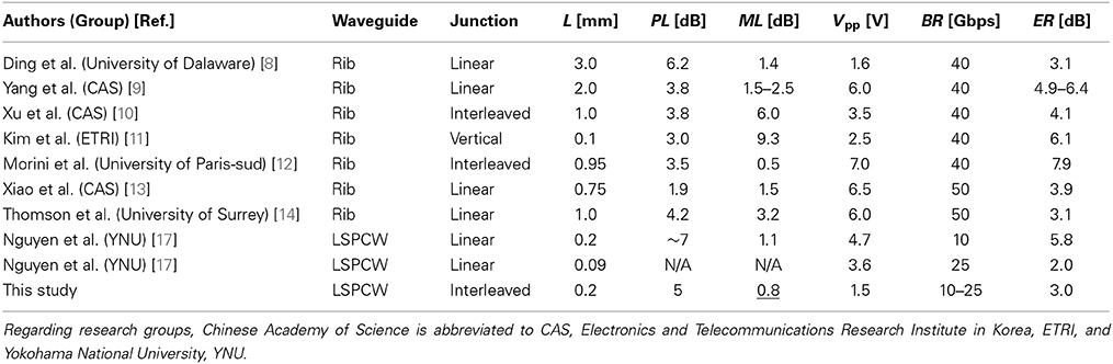
Table 1. Comparison of performances of modulators.
Calculations
Structure
Figure 2 shows the structure of the LSPCW modulator in this study. It consists of two LSPCW phase shifters with p/n junctions at the waveguide center, thermo-optic phase tuners with TiN heaters, and MZ circuit of Si wires. We compare linear and interleaved p/n junction. The phase tuner in our previous studies was formed at the Si wire. In this study, it is located at the LSPCW so that the slow light enhancement is also expected not only for the phase shifter but also for the phase tuner. Structural parameters we can design are L, LSPCW's lattice constant a, hole diameter 2r and lattice shift s, doping concentrations of n, p, n+, and p+ regions, NA, ND, N+A, and N+D, respectively, total width of the p and n regions, W, width between electrodes, W+, and interval wx and width wy of the interleaved junction. Values used for these parameters in this experiment are summarized in Table 2. Fundamentally, we used L = 200 μm and ng = 22 (experimental value shown below) given by the listed values of a, 2r, and s [16, 17]. In addition, we also prepared L = 90 μm samples for comparison. Typical values were employed for N+A, N+D, and W+ [15–17]. We set W = 4 μm to avoid the free carrier absorption loss in p+ and n+ regions [17]. On the other hand, we changed NA, ND, wx, and wy as parameters for investigation.
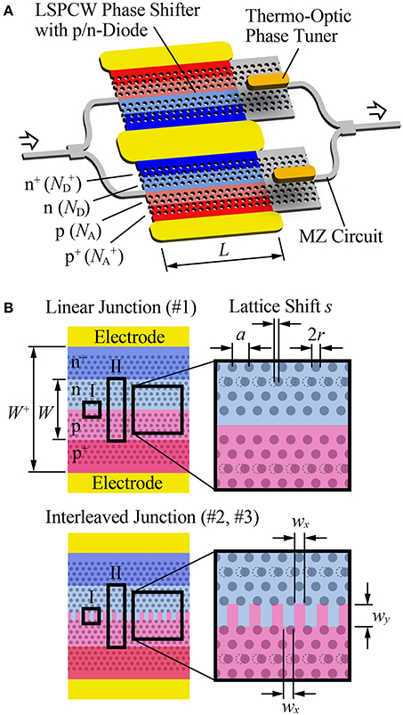
Figure 2. Schematic of Si LSPCW MZ modulator. (A) Total view. (B) Two types of p/n junction. I and II correspond to models in Figures 3, 4, respectively.
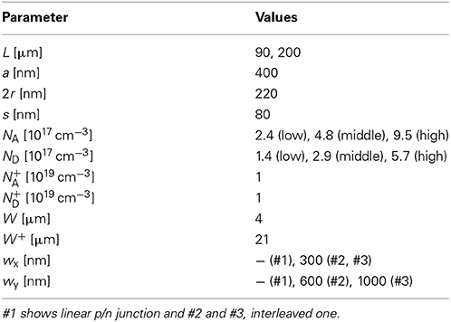
Table 2. Design parameters.
Phase Shift
The phase shift Δϕ of the waveguide mode in a MZ modulator when the voltage is applied to the p/n junction is given by the following:
where Δk is the wavenumber shift of the waveguide mode, k0 = 2π/λ is the wavenumber in vacuum, neq is the modal equivalent index, and Δneq is the change of neq with the voltage. For the transverse-electric (TE) polarized light exhibiting a photonic band gap at λ = 1.55 μm, ng ~20 and neq = 2.33 are obtained for a, 2r, and s values in Table 2. ζ is almost a constant value close to 1, where ωb is the photonic band frequency. Δϕ in Equation (1) becomes twice larger when the push-pull drive is used, which generates the opposite sign of Δneq to the two phase shifters.
Δneq is generated by the local index change of Si, ΔnSi, due to the carrier plasma effect that occurs when the carrier distribution is changed by applying voltage. We calculated the carrier distribution, as shown in Figure 3, using commercial simulator, Lumerical DEVICE. Here, we assume linear p/n junction (device #1) and interleaved one (device #2 in Table 2) and set middle doping concentrations in Table 2. It is clear that the depletion region extends with increasing the reverse bias. Obviously, the interleaved junction produces larger depletion region around the waveguide center. ΔnSi can be estimated by the following formula by Soref and Bennett [26]:
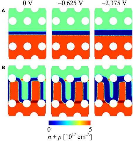
Figure 3. Calculation results of carrier distribution around the center of LSPCW (model I of Figure 2). (A) Device #1 with linear junction. (B) Device #2 with interleaved junction. Blue region shows depletion region.
When the depletion region extends, both Δn [cm−3] and Δp [cm−3] decrease, leading to a positive ΔnSi. Figure 4A shows the spatial distribution of ΔnSi in the unit cell model of LSPCW (II in Figure 2), when the applied voltage is changed from −0.625 to −2.375 V, which correspond to dc bias voltage VDC = −1.50 V and drive voltage Vpp = 1.75 V in the modulation experiment. Here is an example for the linear junction corresponding to Figure 3A. It is observed that ΔnSi is localized at both edges of the depletion region. Negative ΔnSi appeared at some points simply due to numerical imperfection. However, we can neglect it because the number of points exhibiting negative ΔnSi points is limited and the absolute values of negative ΔnSi are much smaller than positive ones. Figure 4B shows the distribution of the waveguide mode, which is calculated by Lumerical FDTD Solutions. Although this distribution can change with ΔnSi, it is negligible. The mode is almost localized at the waveguide center, but penetrates into the third rows of airholes. Eventually, the mode in the LSPCW distributes more widely than that in rib waveguide modulator. Finally, Δneq is given by
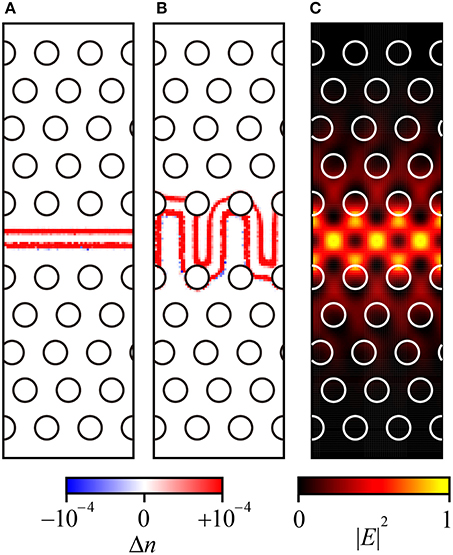
Figure 4. (A,B) Index change of Si in device #1 with linear junction and #2 with interleaved junction (wy = 600 nm), respectively, and (C). Waveguide mode intensity in unit cell model II in Figure 2.
We calculated Δneq for device #1 with the linear junction and devices #2 and #3 with interleaved junctions with wx = 300 nm and wy = 600 or 1000 nm, respectively. The results are summarized in Table 3. Corresponding to the larger depletion region of the interleaved junction #2 and #3, Δneq increases to 1.7 and 2.0 times that of the linear junction, respectively.
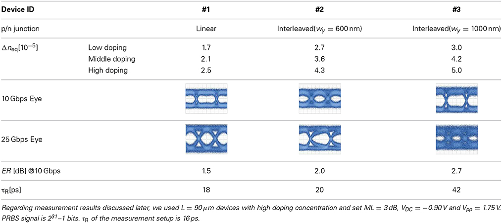
Table 3. Comparison of performance between three p/n junctions.
Similarly, we calculated Δneq for a typical rib waveguide modulator with the central linear junction and middle doping. Assuming the width and height of the rib modulator to be 400 and 210 nm, respectively, and the slab thickness to be 60 nm, Δneq was obtained as 5.0 × 10⁻⁵. Since Δneq in the LSPCW was calculated as 2.1 × 10⁻⁵, Δneq in the LSPCW is 0.42 times that in the rib waveguide. As mentioned above, this is caused mainly by the LSPCW's slow light mode deeply penetrating into the photonic crystal. As ng of the LSPCW and rib waveguide are 22–24 (measrued values shown later) and 4, respectively, ng suggests 5-fold enhancement. However, the efficiency and the enhancement should be evaluated by the product of ng and Δneq. as seen in Equation (5). Eventually, the wider mode of the LSPCW reduces the net slow light enhancement to 2.3–2.5.
Modulation Loss
Figure 5 shows Δϕ and ML calculated for L using Equations (4, 5), assuming the push-pull drive and the same parameters as for Figures 3, 4. Naturally Δϕ increases and ML decreases as L gets longer. The interleaved junction is effective for increasing Δϕ. While ML becomes <1 dB at L as large as 439 μm with the linear junction, it does at L = 255 μm with the interleaved junction (wy = 600 nm) and at L = 219 μm with that (wy = 1000 nm).
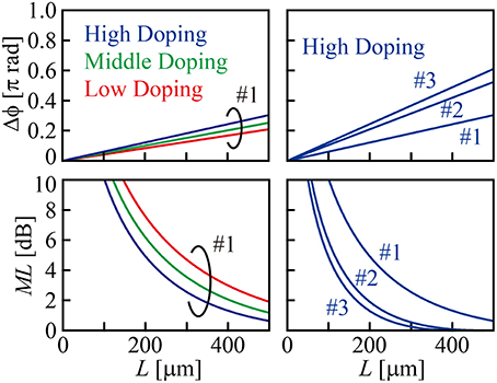
Figure 5. Calculation results of phase shift and modulation loss with phase shifter length for device #1–#3 when ER = 3 dB is assumed. Voltage change is set from −0.625 to −2.375 V.
RC Time Constants
When the electrical resistance and capacitance at electrodes and additional parasitic capacitance are negligible, the operation speed of the modulator is dominated by the RC time constant τRC. The resistance R around the p/n junction can be evaluated from the current for the applied voltage. We calculated it using DEVICE, assuming the same parameters as for Figure 3 and L = 200 μm. Then we obtained resistances for p and n regions to be 58 and 38 Ω, respectively, resulting in R = 96 Ω. This value does not depend much on the junction profile and is determined mainly by the total width of the p and n regions, W. Since we fixed W = 4 μm to avoid the absorption loss as mentioned above, R is hardly reduced even after the fine adjustment of W. The reduction is rather expected by increasing doping concentrations. This R is 3–6 times larger than rib waveguide modulators. This is caused by the wide W originating from the deep field penetration, which is a drawback of slow light.
The junction capacitance C can be evaluated by the relation between the charge accumulated at the junction and the applied voltage V. Figure 6 shows the calculation results of C, τRC, and 3-dB cutoff frequency f3dB. For device #1 with the linear junction, C = 26–50 fF and f3dB = 33–65 GHz are estimated for V from 0 V to −3 V. f3dB increases as more V is applied, while dC/dV decreases, meaning that Δϕ diminishes. C becomes twice for #2 with the interleaved junction (wy = 600 nm) and 2.5–3.1 times for #3 with that (wy = 1000 nm), and the voltage dependence of C increases proportionally. This corresponds the enhancement of Δϕ shown in Section Phase Shift and simultaneously means the reduced bandwidth. Therefore, the optimum voltage and wy exist for a target bandwidth. If we design toward f3dB = 25 GHz, for example, a bias voltage of around −1.5 V is optimum for #2.
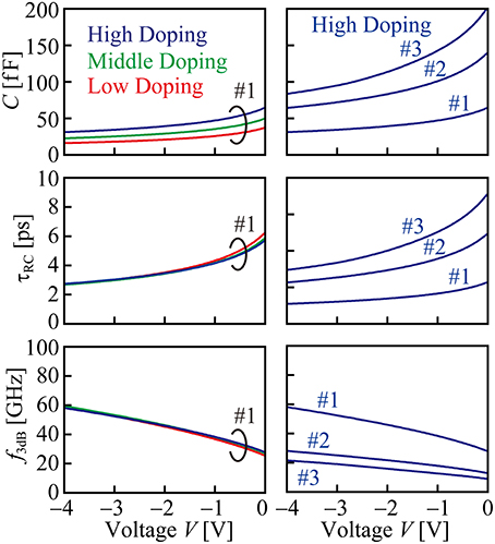
Figure 6. Calculation results of junction capacitance, RC time constant, and 3-dB cutoff frequency for device.
Now, the time constant does not depend on L because R is inversely proportional to and C is proportional to L. Hence, τRC and f3dB similar to those in Figure 6 may be obtainable at different L. Actually, however, the internal resistance of 50 Ω in the modulator driver is included in the whole circuit. On this condition, longer L is not effective for reducing R, thus rather reduces f3dB. Shorter L is more advantageous concerning f3dB, but the decrease in C results in smaller Δϕ and lower ER. Therefore, the careful optimization and balancing are necessary. Anyway, the internal resistance reduces f3dB at any L than that in Figure 6 (for example, ~0.66 times at L = 200 μm). Still 25 Gbps modulation will be possible by employing #1 and #2. For longer L, the phase matching between slow light and rf signal will be another issue, which we will discuss at another instance.
Fabrication and Measurement
For fabrication, we used the foundry service using CMOS-compatible process (minimum linewidth of 180 nm) provided by Institute of Microelectronics, Singapore. Figure 7 shows the fabricated device. The basic structure is the same as that in Figure 2A. p and n regions were formed by boron and phosphorus ion implantations, respectively. As shown in Table 2, three types of doping concentrations were prepared. Electrodes of the phase shifter and phase tuner were 700-nm-thick Al. GSGSG rf probe pad was arranged on the input side, while the termination on the output side was omitted. The phase tuner was shortened to 36.5 from 200 μm in previous studies [16, 17], considering the slow light enhancement. Thermal isolation trenches of more than 50 μm depth were formed around the phase tuner. Figure 8 shows the transmission intensity and ng spectra of the device. The latter was measured by modulation phase shift method. Low-dispersion slow light exhibiting ng = 22–24 and Δλ ~ 14 nm was obtained. Although these spectra were measured for interleaved junction (#2) and high doping concentrations, similar spectra were obtained for other devices. The insertion loss at the transmission peak intensity, estimated by comparing the output intensity with that from the Si wire waveguide of the same length was less than 5 dB, which is lower than 7 dB in the previous studies. It is attributed to the further optimization and loss reduction at the splitter of the MZ circuit and connection between the Si wire and LSPCW. Black circles in Figure 1 show the measured output intensity at each operating point changed by the heater power for this device. The circles are well fitted to the theoretical curve when a 0.02π offset is assumed. This indicates that phase shift is proportional to heater power. This offset and the bottom intensity saturated at −25 dB around ϕ = π suggest that a slight difference between two optical paths was induced by fabrication errors, although it is a trivial problem.
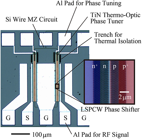
Figure 7. Optical micrograph of fabricated device.
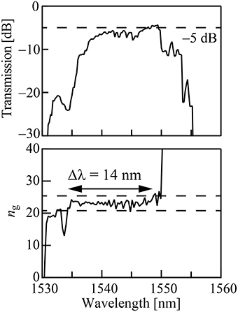
Figure 8. Measured spectra of transmission intensity and group index. The broken line shows the wavelength which was used in the modulation experiment.
In the modulation experiment, we directly applied the same dc bias VDC to the two phase shifters and opposite sign of pseudo-random bit sequence (PRBS) non-return-to-zero (NRZ) signal Vpp (push-pull drive) by using pulse pattern generator Anritsu MG3692B, MP181020A, MP181040A and GSGSG RF probe with a 40 GHz bandwidth. Compared with previous studies, S/N was improved by removing electrical amplifiers and bias tee and shortening rf cables. Input laser light was set at 1555.5 nm, which is the center wavelength of the spectra in Figure 8. It was adjusted to TE by polarization controller, and coupled from lensed fiber to Si inverse-tapered spot size converter, which was integrated on a chip. Modulated light was similarly coupled to another fiber and detected by optical sampling oscilloscope Agilent 86100C, 86109A.
The following measurement results used VDC = −1.5 V, Vpp = 1.75 V, and BR = 25 Gbps as base settings. Figure 9 shows 25 Gbps eye patterns at each operating point in Figure 1. When ϕ is close to 0 (point A), ML and ER are small, resulting in closed eye. When ϕ is close to π (point E), ER becomes large, and S/N is degraded by the large ML. Figure 10 summarizes the dependence on BR, Vpp, and VDC at point D. In A, clear open eye with ER ~ 4 dB is maintained in the range of 10–25 Gbps. As seen in Figure 6, f3dB for device #1 with the linear junction is sufficiently large. Therefore, higher-speed operation will be confirmed if higher speed measurement setup is available. In B, ER is larger at higher Vpp and ER = 3 dB is obtained at Vpp = 1.5 V. In C, ER is increased as VDC approaches to 0 V. Although small VDC generally increases C and decrease the response speed as seen in Figure 6, its influence did not appear because of the sufficient bandwidth of the linear junction.
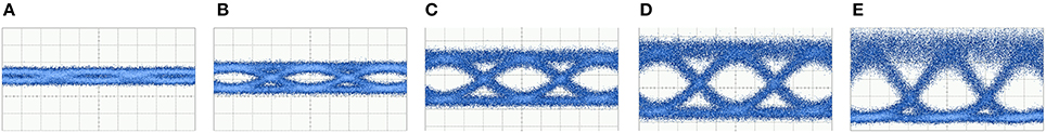
Figure 9. 25-Gbps eye patterns for device #1 with linear junction, middle doping concentration, and L = 200-μm. (A–E) correspond to those in Figure 1. PRBS signal consists of 27–1 bit. Output light was amplified by erbium-doped fiber amplifier and amplified spontaneous emission noise was removed by band pass filter.
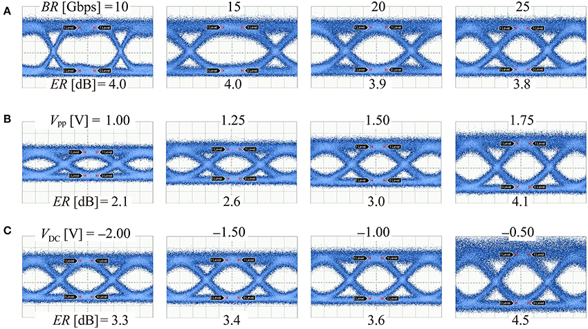
Figure 10. Parameter dependence of the eye pattern for device #1 with liner junction and middle doping concentration. Basic settings, and measurement condition are the same as those for Figure 9, and operating point was set at D (ML = 7 dB) in Figure 1. (A) BR dependence. (B) Vpp dependence. (C) VDC dependence.
In Figure 10, we can observe clear eye patterns from low voltages, but still Δϕ is small and ML is as large as 7 dB. When employing the interleaved junction, Δϕ increases although the response is degraded. Table 3 compares eye patterns, ER and 20–80% rise time τR for #1 with the linear junction and #2 and #3 with interleaved junctions. Due to the limited samples, the devices shown here are all highly doped and have a length of L = 90 μm. We set ML = 3 dB for moderate eye opening; ER is small but we can compare them qualitatively. wx = 200 nm seems to be better because the interval 2wx is the same as a, but actually we observed more closed eye for wx = 200 nm and lower ER, which might be caused by the p/n compensation. Although ER became maximum at wx = 300 nm and wy = 1000 nm, the response was slow, as seen from τR = 42 ps and S/N is particularly degraded at 25 Gbps, which might be caused by the pattern effect. Moderate ER and τR were obtained and clear 25 Gbps open eye was observed at wx = 300 nm and wy = 600 nm.
Figure 11 shows the dependence of ER on the doping concentration in the L = 90 μm device #1 and #2. ER increased at a higher doping concentration for both junctions, and the increase is particularly large in the interleaved junction. The decrease in the transmission intensity, which could occur due to the free carrier absorption, was less than 1 dB even at the high doping concentration. Figure 12 shows 25 Gbps eye pattern in the L = 200 μm device with the interleaved junction and high doping concentration. We observed ER = 3.0 dB simultaneously with ML = 0.8 dB. We observed τR, as short as 19 ps, which indicates higher speed modulation.
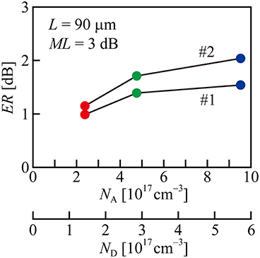
Figure 11. Doping concentration of ER at 10-Gbps (231–1 bits) for device #1 with linear junction and device #2 with interleaved junction (wx = 300 nm, wy = 600 nm).
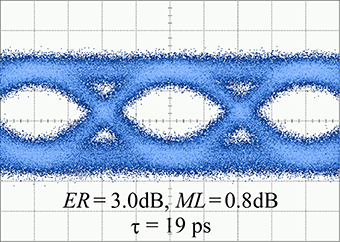
Figure 12. (231–1 bits) eye pattern for L = 200 μm device #2 with interleaved junction (wy = 600 nm) and high doping concentration. Vpp = 1.75 V and VDC = −0.90 V. In this measurement, higher–speed pulse pattern generator (Anritsu 183021A; the measurement τR is 11 ps) was used.
Conclusions
We discussed the index and phase changes in Si LSPCW MZ modulators from theoretical calculations and experiment and estimated that the advantage of slow light is 2.3–2.5 times compared with rib waveguide modulators and that additional enhancement of 1.7–2.0 times is obtainable by employing the interleaved junction and 1.2 times by increasing the doping concentration. Increasing the phase shift lowers the modulation loss. We also discussed the response speed and concluded that the linear junction has a sufficient modulation bandwidth of f3dB = 33–65 GHz and that it decreases to less than half when employing interleaved junctions. We experimentally obtained 25 Gbps clear open eyes with extinction ratios of 3.0–4.1 dB at low voltages of Vpp = 1.50–1.75 V for the L = 200 μm device when 7 dB modulation loss is added. We further obtained the extinction ratio of 3.0 dB even with a modulation loss of 0.8 dB by using optimum interleaved junction and high doping concentration. This performance meets most of the requirements for current and near-future optical interconnects.
Conflict of Interest Statement
The authors declare that the research was conducted in the absence of any commercial or financial relationships that could be construed as a potential conflict of interest.
Acknowledgment
This study was partly supported by New Energy and Industrial Technology Development Organization.
References
1. Reed GT, Mashanovich G, Gardes FY, Thomson DJ. Silicon optical modulators. Nat Photonics (2010) 4:518. doi: 10.1038/nphoton.2010.179
2. Zhou G, Geis MW, Spector SJ, Gan F, Grein ME, Schulein RT, et al. Effect of carrier lifetime on forward-biased silicon Mach-Zehnder modulators. Opt Express (2008) 21:11869. doi: 10.1364/OE.16.005218
Pubmed Abstract | Pubmed Full Text | CrossRef Full Text | Google Scholar
3. Akiyama S, Imai M, Baba T, Akagawa T, Hirayama N, Noguchi Y, et al. Compact PIN-diode-based silicon modulator using side-wall-grating waveguide. IEEE J Sel Top Quantum Electron. (2014) 19:3401611. doi: 10.1109/JSTQE.2013.2278438
Pubmed Abstract | Pubmed Full Text | CrossRef Full Text | Google Scholar
4. Baba T, Akiyama S, Imai M, Hirayama N, Takahashi H, Noguchi Y, et al. 50-Gb/s ring-resonator-based silicon modulator. Opt Express (2013) 21:11869. doi: 10.1364/OE.21.011869
Pubmed Abstract | Pubmed Full Text | CrossRef Full Text | Google Scholar
5. Nguyen HC, Sakai Y, Shinkawa M, Ishikura N, Baba T. 10 Gb/s operation of photonic crystal silicon optical modulators. Opt Express (2012) 19:13000. doi: 10.1364/OE.19.013000
Pubmed Abstract | Pubmed Full Text | CrossRef Full Text | Google Scholar
6. Timurdogan E, Sorace-Agaskar CM, Sun J, Hosseini S, Biberman A, Watts MR. An ultralow power athermal silicon modulator. Nat Commun. (2014) 5:4008 doi: 10.1038/ncomms5008
Pubmed Abstract | Pubmed Full Text | CrossRef Full Text | Google Scholar
7. Xiao X, Xu H, Li X, Hu Y, Xiong K, Li Z, et al. 25 Gbit/s silicon microring modulator based on misalignment-tolerant interleaved PN junctions. Opt Express (2012) 20:2507. doi: 10.1364/OE.20.002507
Pubmed Abstract | Pubmed Full Text | CrossRef Full Text | Google Scholar
8. Ding R, Liu Y, Li Q, Yang Y, Ma Y, Padmaraju K, et al. Design and characterization of a 30-GHz bandwidth low-power silicon traveling-wave modulator. Opt Commun. (2014) 321:124. doi: 10.1016/j.optcom.2014.01.071
9. Yang L, Ding J. High-speed silicon Mach–Zehnder optical modulator with large optical bandwidth. J Lightwave Technol. (2014) 32:966. doi: 10.1109/JLT.2013.2295401
10. Xu H, Li X, Xiao X, Li Z, Yu Y, Yu J. Demonstration and characterization of high-speed silicon depletion-mode Mach–Zehnder modulators. IEEE J Sel Top Quantum Electron. (2014) 20:3400110. doi: 10.1109/JSTQE.2013.2293763
11. Kim G, Park JW, Kim IG, Kim S, Jang K, Kim SA, et al. Compact-sized high-modulation-efficiency silicon Mach–Zehnder modulator based on a vertically dipped depletion junction phase shifter for chip-level integration. Opt Lett. (2014) 39:2310. doi: 10.1364/OL.39.002310
Pubmed Abstract | Pubmed Full Text | CrossRef Full Text | Google Scholar
12. Marris-Morini D, Baudot C, Fédéli JM, Rasigade G, Vulliet N, Souhaité A, et al. Low loss 40 Gbit/s silicon modulator based on interleaved junctions and fabricated on 300 mm SOI wafers. Opt Express (2013) 21:22471. doi: 10.1364/OE.21.022471
Pubmed Abstract | Pubmed Full Text | CrossRef Full Text | Google Scholar
13. Xiao X, Xu H, Li X, Li Z, Chu T, Yu Y, et al. High-speed, low-loss silicon Mach-Zehnder modulators with doping optimization. Opt Express (2013) 21:4116. doi: 10.1364/OE.21.004116
Pubmed Abstract | Pubmed Full Text | CrossRef Full Text | Google Scholar
14. Thomson DJ, Gardes FY, Fedeli J, Zlatanovic S, Hu Y, Kuo BPP, et al. 50-Gb/s silicon optical modulator. IEEE Photonics Technol Lett. (2012) 24:234. doi: 10.1109/LPT.2011.2177081
15. Nguyen HC, Sakai Y, Shinkawa M, Ishikura N, Baba T. Photonic crystal silicon optical modulators: carrier-injection and depletion at 10 Gb/s. IEEE J Quantum Electron. (2012) 48:210. doi: 10.1109/JQE.2011.2174338
16. Nguyen HC, Hashimoto S, Shinkawa M, Baba T. Compact and fast photonic crystal silicon optical modulators. Opt Express (2012) 20:22465. doi: 10.1364/OE.20.022465
Pubmed Abstract | Pubmed Full Text | CrossRef Full Text | Google Scholar
17. Nguyen HC, Yazawa N, Hashimoto S, Otsuka S, Baba T. Sub-100 μm photonic crystal Si optical modulators: spectral, athermal and high-speed performance. IEEE J Sel Top Quantum Electron. (2013) 19:3400811. doi: 10.1109/JSTQE.2013.2265193
18. Xu H, Xiao X, Li X, Hu Y, Li Z, Chu T, et al. High speed silicon Mach-Zehnder modulator based on interleaved PN junctions. Opt Express (2012) 20:15093. doi: 10.1364/OE.20.015093
Pubmed Abstract | Pubmed Full Text | CrossRef Full Text | Google Scholar
19. Yu H, Pantouvaki M, Campenhout JV, Korn D, Komorowska K, Dumon P, et al. Performance tradeoff between lateral and interdigitated doping patterns for high speed carrier-depletion based silicon modulators. Opt Express (2012) 20:12926. doi: 10.1364/OE.20.012926
Pubmed Abstract | Pubmed Full Text | CrossRef Full Text | Google Scholar
20. Kim Y, Takenaka M, Osada T, Hata M, Takagi S. Strain-induced enhancement of plasma dispersion effect and free-carrier absorption in SiGe optical modulators. Sci Rep. (2014) 4:4683. doi: 10.1038/srep04683
Pubmed Abstract | Pubmed Full Text | CrossRef Full Text | Google Scholar
21. Liu J, Beals M, Pomerene A, Bernardis S, Rong S, Cheng J, et al. Waveguide-integrated, ultra-energy GeSi electro-absorption modulators. Nat Photonics (2008) 2:433. doi: 10.1038/nphoton.2008.99
22. Baba T. Slow light in photonic crystals. Nat Photonics (2008) 2:465. doi: 10.1038/nphoton.2008.146
23. Baba T, Nguyen HC, Ishikura N, Suzuki K, Shinkawa M, Hayakawa R, et al. Photonic crystal slow light devices fabricated by CMOS-compatible process. IEICE Electron Express (2013) 10:1. doi: 10.1587/elex.10.20132002
24. Hamachi Y, Kubo S, Baba T. Slow light with low dispersion and nonlinear enhancement in a lattice-shifted photonic crystal waveguide. Opt Lett. (2009) 34:1072. doi: 10.1364/OL.34.001072
Pubmed Abstract | Pubmed Full Text | CrossRef Full Text | Google Scholar
25. Li Z, Xu D, McKinnon WR, Janz S, Schmid JH, Cheben P, et al. Silicon waveguide modulator based on carrier depletion in periodically interleaved PN junctions. Opt Express (2009) 17:15947. doi: 10.1364/OE.17.015947
Pubmed Abstract | Pubmed Full Text | CrossRef Full Text | Google Scholar
26. Soref RA, Bennett BR. Electrooptical effects in silicon. IEEE J Quantum Electron. (1987) QE-23:123. doi: 10.1109/JQE.1987.1073206
Pubmed Abstract | Pubmed Full Text | CrossRef Full Text | Google Scholar
Keywords: silicon photonics, modulator, photonic crystal waveguides, optoelectronics, slow light
Citation: Terada Y, Ito H, Nguyen HC and Baba T (2014) Theoretical and experimental investigation of low-volgage and low-loss 25-Gbps Si photonic crystal slow light Mach–Zehnder modulators with interleaved p/n junction. Front. Phys. 2:61. doi: 10.3389/fphy.2014.00061
Received: 02 September 2014; Accepted: 13 October 2014;
Published online: 06 November 2014.
Edited by:
Kensuke Ogawa, Fujikura Ltd., JapanReviewed by:
Satoshi Iwamoto, The University of Tokyo, JapanTakasumi Tanabe, Keio University, Japan
Copyright © 2014 Terada, Ito, Nguyen and Baba. This is an open-access article distributed under the terms of the Creative Commons Attribution License (CC BY). The use, distribution or reproduction in other forums is permitted, provided the original author(s) or licensor are credited and that the original publication in this journal is cited, in accordance with accepted academic practice. No use, distribution or reproduction is permitted which does not comply with these terms.
*Correspondence: Toshihiko Baba, Department of Electrical and Computer Engineering, Yokohama National University, 79-5 Tokiwadai, Hodogayaku, Yokohama, Kanagawa 240-8501, Japan e-mail: baba@ynu.ac.jp