High-speed and efficient silicon modulator based on forward-biased pin diodes
 Suguru Akiyama*
  Tatsuya Usuki
- Photonics Electronics Technology Research Association, Tsukuba, Japan
Silicon modulators, which use the free-carrier-plasma effect, were studied, both analytically and experimentally. It was demonstrated that the loss-efficiency product, α · VπL, was a suitable figure of merit for silicon modulators that enabled their intrinsic properties to be compared. Subsequently, the dependence of VπL on frequency was expressed by using the electrical parameters of a phase shifter when the modulator was operated by assuming a simple driving configuration. A diode-based modulator operated in forward biased mode was expected from analyses to provide more efficient operation than that in reversed mode at high frequencies due to its large capacitance. We obtained an α · VπL of 9.5 dB·V at 12.5 GHz in experiments by using the fabricated phase shifter with pin diodes operated in forward biased mode. This α · VπL was comparable to the best modulators operated in depletion mode. The modulator exhibited a clear eye opening at 56 Gb/s operated by 2 V peak-to-peak signals that was achieved by incorporating such a phase shifter into a ring resonator.
Introduction
Total transmission capacity urgently needs to be scaled up for transceivers in optical fiber communications [1–5]. Increasing the channel rate with the baud rate or using multi-level modulation is relatively simple since numbers of photonic and electronic devices inside the transceiver remain constant. The bit rate on a single optical carrier has already exceeded 100 Gb/s [1–3, 6–9]. Even when these wide-bandwidth technologies are used, it is necessary to use parallel links [4], wavelengths [1, 5, 10, 11] or polarization multiplexing [3, 6–8, 12], or combinations of them, to reach the targets of the next and future generations of transceivers, such as 400 Gb/s and 1 Tb/s. In any case, the numbers of electronic and photonic devices will both increase. High levels of integration of devices will likely be introduced to transceivers to ensure they are compact. Silicon photonics have been extensively studied in the past decade because they can potentially enable such photonic integrated circuits [3, 5–42] to be fabricated. Modulators based on silicon substrates are key building blocks in integrated transceivers, which convert high-speed signals from electrical into optical form.
Various kinds of modulators have been proposed and demonstrated, thus far [3, 6, 8, 9, 15, 19–40]. Those using the free-carrier plasma (FCP) effect [41] are particularly suitable for integrated transceivers because they are made with materials and by processes that are compatible with those of standard silicon electronic devices. This means high levels of integration are possible for these silicon modulators in manufacturing them [11, 17, 18]. These modulators need electric capacitors, which can dynamically store and release electrons and/or holes at the waveguide core. Thus, far, forward [20–26] and reverse-biased [20, 27–34] pn diodes, and MOS capacitors operated in accumulation mode [35–38] have been implemented, and such devices have all demonstrated high-speed operations above 40 Gb/s with reasonably small driving voltages and footprints. Modulators that are superior in terms of fundamental performance should be chosen to meet the requirements of continuously increasing data rates of transceivers. They should be chosen to provide a specific optical modulation amplitude (OMA) at a given operating speed using the smallest driving voltage and footprint. However, these parameters are related trade-offs and depend on operating conditions, such as driver circuits and input optical power. Therefore, it is difficult to compare the intrinsic performance of modulators under fair and reasonable assumptions.
We found that the loss-efficiency product, α · VπL [28], at a given operating frequency was a suitable figure of merit (FOM) for silicon modulators to enable their intrinsic characteristics to be compared. We analytically derived the expression of α · VπL using more fundamental parameters of phase shifters, such as propagation loss, electric capacitance and resistance, and Qπ [42]; Qπ means the amount of charge needed to cause π phase shift of light in the waveguide. Modulators based on forward and reverse-biased pn diodes were compared in light of this analysis. We expected that forward-biased diodes would provide larger modulation efficiency and comparable propagation loss than reverse-biased diodes. The measured parameters for FOM were found by using fabricated silicon modulators based on forward-biased pin diodes and they are presented in the latter part of this paper. The α · VπL of the fabricated modulator was 9.5 dB·V at 12.5 GHz, which is comparable to that of the best depletion-type modulators [30] and better than that of most modulators. Finally, we conducted experiments on 56-Gb/s large-signal modulation by using the modulators we fabricated based on a ring resonator. A clear eye-opening was obtained by using pre-emphasis signals with a driving voltage of about 2 volt-peak-to-peak (Vpp).
Analysis
This section defines suitable FOM for the modulator, and its derived expression using parameters that characterize the phase shifter itself. We compared the properties of modulators on the basis of analyses based on forward and reverse-biased diodes toward achieving high-speed and efficient modulation.
α·V πL as FOM of Modulator
Figure 1 outlines the configuration for the Mach-Zehnder (MZ) modulator that we analyzed. This simple figure covers most of the important parameters both as resources that the modulator uses and functions that it provides. Provided that the operating speed is a given condition, the only output from the modulator is OMA (ΔP). However, the modulator needs a footprint that is the length of the phase shifter (l), input optical power (Pin), and driving voltage with an amplitude of ΔV as resources. We excluded l from FOM in these parameters. As transceivers are much larger than modulator chips in most cases, l itself was not a significant factor. The modulator response is usually proportional to Pin, and we used Δr = ΔP/Pin instead of the two parameters. The value of Δr depends on ΔV. Our point of view is that the best modulator provides the minimum ΔV for a given Δr. Our first aim was to express the relation between these two using inherent parameters of the modulator.
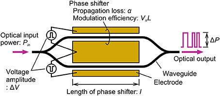
Figure 1. Configuration of analyzed MZ modulator. Two phase shifters in MZ interferometer are driven with voltage amplitude of ΔV in push-pull configuration.
This task is straightforward in DC operation. When the MZ modulator is driven around a quadrature phase difference of π/2 and in a push-pull configuration, the result is
The above formula includes three parameters of the phase shifter, which are optical propagation loss (α) in dB, voltage-length-product (VπL), and the length of the phase shifter (l). The Δr becomes maximum at certain l. Such Δrmax and lmax are
Thus, α · VπL determines the maximum OMA for a given ΔV and Pin, and is a suitable FOM for modulators. Figure 2 plots the calculated results of Δrmax and αlmax for a different k. As expected, the smaller k is, the larger the Δrmax that can be obtained. When the technology for the driver circuit and performance of the modulator are given, Δrmax can be calculated from the corresponding k by using Figure 2. This enables the optical links to be designed in terms of the power budget. Optimum l can also be obtained from the graph. Note that αlmax reaches 10/ln(10) ≈ 4.34 dB when k is large and Δrmax is relatively small.
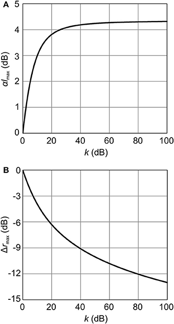
Figure 2. (A) Product of propagation loss and length of phase shifter at which maximum Δr is obtained, as function of k = α · VπL/ΔV. (B) Maximum Δr obtained from modulator as function of k.
Dependencies of αVπL on Fundamental Parameters of Phase Shifter
Next, let us consider the analysis of high-frequency operation for the MZ modulator. Figure 3 outlines the driving configuration for the phase shifter that we assumed for the analysis. The phase shifter, with a total length of l, is divided into N-small-phase shifters, so that they can behave as electrically lumped elements [37]. All phase shifters are expressed as simple resistance-capacitance (RC) circuits connected in series. We also assumed that driving signals would be applied to each small phase shifter with suitable delay between adjacent small phase shifters. By assuming this, we neglected the roll-off of frequency response of the modulator that was caused by the velocity mismatch between the light and electrical signals. This configuration can be applied to any type of capacitance that the modulator uses, including that by forward and reverse-biased pn diodes, and MOS capacitances. After this, we will derive the VπL for amplitude ΔV of signal sources in Figure 3, which vary at angular frequency ω.
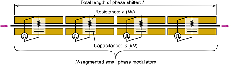
Figure 3. Driving configuration of phase shifter for high-speed operation. Phase shifter is divided into N-small phase shifters. Each phase shifter is considered as simple RC lumped circuit and operated by signal source with suitable signal delay between them.
First, the amount of charge that is dynamically stored in the capacitance of each segmented phase shifter is expressed as
Here, c and ρ correspond to capacitance and series resistance of the phase shifter per unit length. The phase shift obtained from the whole phase shifter is
Qπ means the amount of charge needed to cause π phase shift of light in the waveguide [42]. Qπ is determined by the field distribution of propagating light and applied electrical signal, and the overlap integral of them. We obtain VπL at ω as
VπL at high frequency does not depend on l. Therefore, we can use the results from DC analysis presented in Subsection α · VπL as FOM of modulator. Consequently, we obtain the FOM of the modulator by combining propagation loss α and the above frequency-dependent VπL.
The above FOM determines the required voltage amplitude, ΔV, for given Δr = ΔP/Pin at operating angular frequency ω in the same manner as DC. The α · VπL is calculated from α, Qπ, ρ, and c for a given frequency; these parameters are essential for modulators.
We compare the operation of an identical phase shifter based on pn diodes operated in forward and reverse-biased modes in the following discussion. Only capacitance significantly varies with the bias voltage in this case, and the other parameters, such as α, Qπ, and ρ, largely remain constant. Figure 4 plots part of the FOM, /, as a function of ω for different c. We used 4 Ω·mm as ρ and 0.45 pF/mm as c for reverse biased operation. We chose these values from typical reported modulators operated in reversed biased mode [15, 30, 31]. For forward biased mode, we used the same ρ as the reversed mode, and 45 pF/mm as c, which was hundred times larger than the reversed mode. As Figure 4 indicates, the response is flat up to the very high frequency due to the small capacitance, but is small compared with forward-biased operations for the reverse-biased mode. The forward-biased mode, on the other hand, provides larger response in the frequency range of the figure. The response follows the line of (ωρ)−1 above the cut-off frequency, which is only about 1 GHz. This means that diode capacitance is almost shunted at those frequencies, and the maximum available current flows in the capacitance exploiting the full capability of the circuit. When ωρc >> 1 above the cut-off frequency, FOM becomes proportional to the product of αQπρ, as shown at the rightmost side in the last equation. Forward-bias operation provides more efficient operation than the reverse [25, 26] by using suitable frequency compensation.
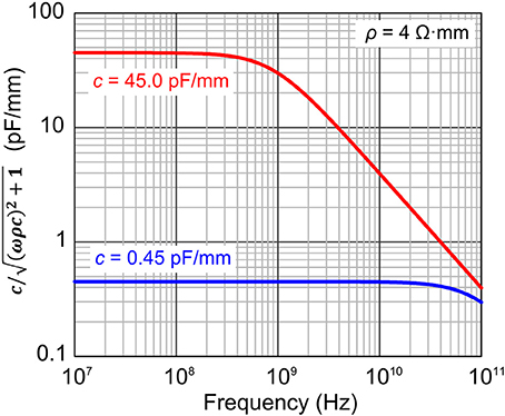
Figure 4. Dependence of c/ on frequency, which is a part of VπL. Forward (red) and reverse (blue) biased operations are assumed.
Characterization of Fabricated Modulator
Device Description
We evaluated the forward biased operation mode by using fabricated silicon modulators based on pin diodes. The experimental results are presented in this subsection. Figure 5 has schematic views of the device we used in the experiments [23–26]. Modulators based on an asymmetric MZ interferometer [25] and a ring resonator [24] were respectively used in the experiment to extract the parameters and achieve high-speed large signal modulation. These experiments are described in the sections that follow in series. Figure 5 outlines the detailed structure of the phase shifter we used in both experiments. We used a waveguide with side-wall gratings, in which narrow fins were periodically placed on both sides of the core as the electrical channel between the core and electrode. The waveguide incorporated pin diodes, where the center of the waveguide core remained un-doped. This waveguide had a couple of advantages over conventional rib waveguides. First, the waveguide could be connected to other photonic components without having to use mode converters. Our modulator had a simple rectangular waveguide at the optical input/output interfaces like the other photonic components, whereas the rib waveguide had thin slab layers on both sides of the core. Second, our waveguide was expected to have a better wafer-to-wafer yield than rib waveguides. The top of the buried oxide layer acted as a stopper for our waveguide in the etching process for the silicon waveguide, whereas the etching duration needed to be precisely controlled to retain slabs with the required thickness for the rib waveguide. The fins were as narrow as several tens of millimeters. We fabricated this device by using an ArF immersion exposure system and other conventional silicon processes for complementary metal–oxide–semiconductor (CMOS) circuits on 300-mm silicon on insulator (SOI) wafers.
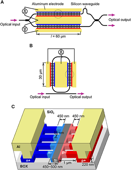
Figure 5. Fabricated (A) MZ modulator and (B) microring modulator. (C) Detailed structure of phase shifter indicated as close ups of dotted circles in (A) and (B).
Extraction of Parameters
First, we measured the dependence of optical insertion loss on the length of the phase shifter. We obtained a propagation loss of 5.3 dB/mm by linear fitting. Next, we extracted the electrical parameters, such as c and ρ, of the phase shifter. We measured the S11 electrical reflections from the phase shifter. As we used a short, 60-μm-long phase shifter, we could treat it as a lumped element. We applied a forward bias voltage of +0.85 V, which was the same as that used in the high-speed operations discussed in the next subsection. The measured and fitted S11 are plotted in Figure 6A. The measured curve was nicely fitted by the equivalent circuit and the electrical parameters, which are shown in Figure 6B. Figure 6C plots both the measured and calculated optical frequency response of the modulator. We calculated optical response as dependence of the amount of stored charge at capacitance in the equivalent circuit on the frequency, when the circuit was driven in a 50-Ω system. Both the measured and calculated results coincided very well, which demonstrated the validity of the assumed equivalent circuit. The c was calculated to be 42.5 pF/mm and ρ was calculated to be 3.68 Ω mm from the equivalent circuit in Figure 6C for the 60-μm-long phase shifter.
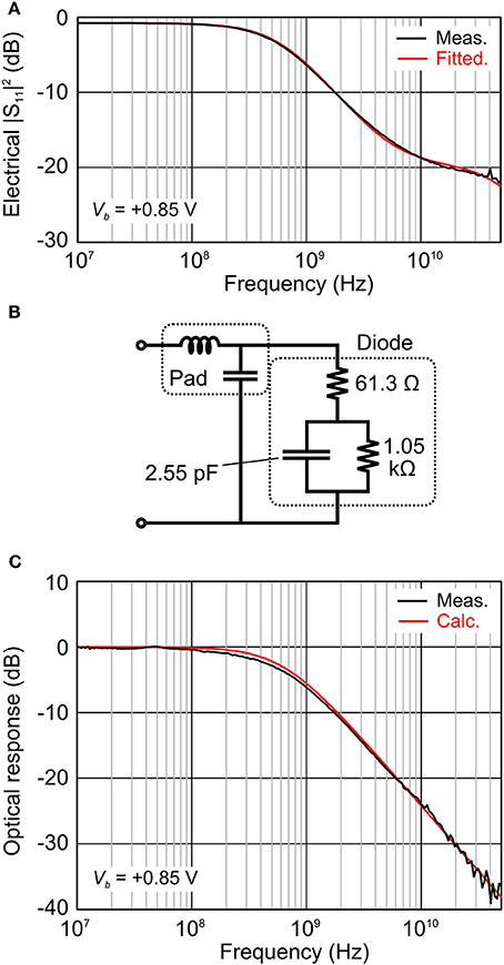
Figure 6. (A) Measured electrical S11 parameter (black) of 60-μm long phase shifter with fitted curve (red) by using extracted equivalent circuit shown in (B). (C) Measured (black) and calculated (red) optical frequency response of MZ modulator. Optical response was calculated as dependencies of amount of stored charge in diode capacitance on frequency.
We first extracted VπL from the shift in the transmission spectrum of the asymmetric MZ modulator to estimate Qπ, when changing bias voltages were applied to the phase shifter around +0.85 V. Let us consider product of voltage applied to the phase shifter and the length of it. When the product is equal to the VπL of the phase shifter, π phase shift is obtained from the definition and charge of c · VπL is stored in the capacitance of the phase shifter. Therefore,
where c is capacitance per unit length of the phase shifter, which is the same as what we extracted from the measured S11. Using the measured VπL of 0.014 V·cm and c of 42.5 pF/mm, we obtained a Qπ of 6.21 pC.
We can calculate α · VπL = ω · αQπρ for a given operating frequency from the extracted parameters. The α · VπL at 12.5 GHz for 25-Gb/s operations approximately determines the overall response of the modulator. We achieved α · VπL = 9.5 dB·V at 12.5 GHz for our phase shifter. If we had used the driver circuit, which had the same output impedance as the series resistance of the phase shifter, ρ should have doubled. The final result for α · VπL in this case should also have doubled. In any case, this α · VπL was comparable to the best outcome for silicon modulators operated in depletion mode, and was better than most of them.
High-Speed Operations
We conducted a high-speed large-signal modulation experiment, by using the phase shifter described in the previous subsection. The lmax was about 800 μm for our phase shifter, with which the series resistance of the device was about 4.5 Ω. A driver amplifier with comparable or smaller output impedance was suitable for that phase shifter to drive; otherwise the output impedance of the driver would have limited the current flow into the phase shifter. However, only a single drive amplifier with 50-Ω output impedance was available in the experiment. Therefore, we used a 60-μm phase shifter, which had series resistance of about 61 Ω. Further, we embedded the phase shifter into a ring resonator to increase the effective optical interaction length, as Figure 5B shows. We used pre-emphasis signals to compensate for the frequency response of the modulator in forward-biased mode, which were generated by a finite-impulse-response (FIR) filter from standard non-return-to-zero (NRZ) signals in a pseudo-random bit sequence (PRBS) of 27-1 [21, 23, 25]. The rate of the pre-emphasis signals was 56 Gb/s and their amplitude was about 2 Vpp. Figure 7 shows the optical output waveform from the modulator, where clear eye openings that were successfully obtained at 56 Gb/s can be seen.
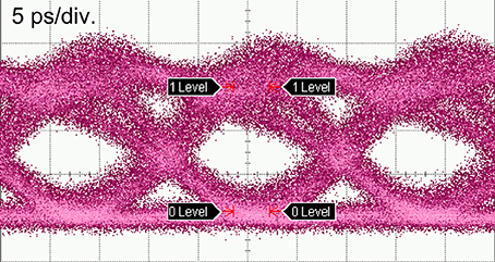
Figure 7. 56-Gb/s optical output waveform obtained by using microring modulator in Figure 5B.
Conclusion
We investigated silicon modulators that utilize the FCP effect. We found that the loss-efficiency product at a given operating frequency is a suitable figure of merit (FOM) for silicon modulators to enable their intrinsic characteristics to be compared. The α · VπL determined the required driving voltage to obtain a specific OMA for a given optical input power to the modulator. From a detailed analysis of FOM, modulators based on forward biased pn diodes are expected to provide more efficient operation than those in the reversed mode, from DC to frequencies higher than 10 GHz, due to the relatively large capacitance. The series resistance of the device in this case is the only factor that limits dynamic current flow into the waveguide core, and a simple form is derived for FOM as α · VπL = ω · αQπρ. We characterized fabricated silicon modulators based on forward-biased pin diodes. The measured α · VπL of the fabricated modulators was 9.5 dB·V at 12.5 GHz, which is comparable to that of the best depletion-type modulators and better than that of most of these modulators. A modulator that used a ring resonator exhibited a clear eye opening at 56 Gb/s in a large signal modulation experiment obtained by using 2-Vpp pre-emphasis signals in forward-biased operation.
Conflict of Interest Statement
The authors declare that the research was conducted in the absence of any commercial or financial relationships that could be construed as a potential conflict of interest.
Acknowledgments
The authors would like to thank staff at TIA-SCR Management Office, AIST for technical support and device fabrication. Part of this research was based on knowledge acquired from the Photonics-Electronics Convergence System Technology (PECST) project. This research was partly supported by the New Energy and Industrial Technology Development Organization (NEDO).
References
1. Tanaka T, Nishihara M, Takahara T, Yan W, Li L, Tao Z, et al. Experimental demonstration of 448-Gbps+ DMT transmission over 30-km SMF. In: Optical Fiber Communication Conference. San Francisco, CA (2014) M2I.5. doi: 10.1364/OFC.2014.M2I.5
2. Iglesias OM, Tianjian Z, Jensen JB, Qiwen Z, Xu X, Monroy IT. Towards 400GBASE 4-lane solution using direct detection of MultiCAP signal in 14 GHz bandwidth per lane. In: Optical Fiber Communication Conference and Exposition and the National Fiber Optic Engineers Conference. Washington, DC: OSA (2013) PDP5C.10. doi: 10.1364/NFOEC.2013.PDP5C.10
3. Dong P, Liu X, Sethumadhavan C, Buhl LL, Aroca R, Baeyens Y, et al. 224-Gb/s PDM-16-QAM modulator and receiver based on silicon photonic integrated circuits. In: Optical Fiber Communication Conference and Exposition and the National Fiber Optic Engineers Conference. Washington, DC: OSA (2013) PDP5C.6. doi: 10.1364/NFOEC.2013.PDP5C.6
4. Schow CL, Doany FE, Rylyakov AV, Lee BG, Jahnes CV, Kwark YH, et al. A 24-channel, 300 Gb/s, 8.2 pJ/bit, full-duplex fiber-coupled optical transceiver module based on a single “Holey” CMOS IC. J Light Technol. (2011) 29:542–53. doi: 10.1109/JLT.2010.2101580
5. Davenport M, Bauters J, Piels M, Chen A, Fang A, Bowers JE. A 400 Gb/s WDM receiver using a low loss silicon nitride AWG integrated with hybrid silicon photodetectors. In: Optical Fiber Communication Conference and Exposition and the National Fiber Optic Engineers Conference. Washington, DC: OSA (2013) PDP5C.5. doi: 10.1364/NFOEC.2013.PDP5C.5
6. Milivojevic B, Raabe C, Shastri A, Webster M, Metz P, Sunder S, et al. 112 Gb/s DP-QPSK transmission Over 2427 km SSMF using small-size silicon photonic IQ modulator and low-power CMOS driver. In: Optical Fiber Communication Conference and Exposition and the National Fiber Optic Engineers Conference. Washington, DC: OSA (2013) OTh1D.1. doi: 10.1364/OFC.2013.OTh1D.1
7. Doerr CR, Chen L, Vermeulen D, Nielsen T, Azemati S, Stulz S, et al. Single-chip silicon photonics 100-Gb/s coherent transceiver. In: Optical Fiber Communication Conference: Postdeadline Papers. Washington, DC: OSA (2014) Th5C.1. doi: 10.1364/OFC.2014.Th5C.1
8. Goi K, Kusaka H, Oka A, Ogawa K, Liow T-Y, Tu X, et al. 128-Gb/s DP-QPSK using low-loss monolithic silicon IQ modulator integrated with partial-rib polarization rotator. In: Optical Fiber Communication Conference. San Francisco, CA (2014) 1:W1I.2. doi: 10.1364/OFC.2014.W1I.2
9. Chagnon M, Osman M, Poulin M, Latrasse C, Gagné J-F, Painchaud Y, et al. Experimental study of 112 Gb/s short reach transmission employing PAM formats and SiP intensity modulator at 13 μm. Opt Express (2014) 22:21018. doi: 10.1364/OE.22.021018
Pubmed Abstract | Pubmed Full Text | CrossRef Full Text | Google Scholar
10. Zheng X, Chang E, Shubin I, Li G, Luo Y, Yao J, et al. A 33 mW 100 Gbps CMOS silicon photonic WDM transmitter using off-chip laser sources. In: Optical Fiber Communication Conference and Exposition and the National Fiber Optic Engineers Conference. Washington, DC: OSA (2013) PDP5C.9. doi: 10.1364/NFOEC.2013.PDP5C.9
11. Jeong S-H, Shimura D, Simoyama T, Seki M, Yokoyama N, Ohtsuka M, et al. Low-loss, flat-topped and spectrally uniform silicon-nanowire-based 5th-order CROW fabricated by ArF-immersion lithography process on a 300-mm SOI wafer. Opt Express (2013) 21:30163–74. doi: 10.1364/OE.21.030163
Pubmed Abstract | Pubmed Full Text | CrossRef Full Text | Google Scholar
12. Taillaert D, Borel PI, Frandsen LH, De La Rue RM, Baets R. A compact two-dimensional grating coupler used as a polarization splitter. IEEE Photonics Technol Lett. (2003) 15:1249–51. doi: 10.1109/LPT.2003.816671
13. Kimerling LC, Ann D, Apsel AB, Beats M, Carothers D, Chen Y-K, et al. Electronic-photonic integrated circuits on the CMOS platform. In: Proceedings of SPIE-The International Society for Optical Engineering. (2013) PDP5C.9, 612502.1–612502.10. Available at: http://cat.inist.fr/?aModele=afficheN&cpsidt=18163096 [Accessed September 10, 2014].
14. De Dobbelaere P, Ayazi A, Chi Y, Dahl A, Denton S, Gloeckner S, et al. Packaging of silicon photonics systems. In: Optical Fiber Communication Conference. Washington, DC: OSA (2012) W3I.2. doi: 10.1364/OFC.2014.W3I.2
15. Li J, Li G, Zheng X, Raj K, Krishnamoorthy AV, Buckwalter JF. A 25-Gb/s monolithic optical transmitter with micro-ring modulator in 130-nm SoI CMOS. IEEE Photonics Technol Lett. (2013) 25:1901–3. doi: 10.1109/LPT.2013.2279509
16. Urino Y, Noguchi Y, Noguchi M, Imai M, Yamagishi M, Saitou S, et al. Demonstration of 12.5-Gbps optical interconnects integrated with lasers, optical splitters, optical modulators and photodetectors on a single silicon substrate. Opt Express (2012) 20:B256–63. doi: 10.1364/OE.20.00B256
Pubmed Abstract | Pubmed Full Text | CrossRef Full Text | Google Scholar
17. Marris-Morini D, Virot L, Baudot C, Fédéli J-M, Rasigade G, Perez-Galacho D, et al. A 40 Gbit/s optical link on a 300-mm silicon platform. Opt Express (2014) 22:6674. doi: 10.1364/OE.22.006674
Pubmed Abstract | Pubmed Full Text | CrossRef Full Text | Google Scholar
18. Selvaraja SK, De Heyn P, Winroth G, Ong P, Lepage G, Cailler C, et al. Highly uniform and low-loss passive silicon photonics devices using a 300 mm CMOS platform. In: Optical Fiber Communication Conference. Washington, DC: OSA (2003) Th2A.33. doi: 10.1364/OFC.2014.Th2A.33
19. Reed GT, Mashanovich G, Gardes FY, Thomson DJ. Silicon optical modulators. Nat Photonics (2010) 4:518–26. doi: 10.1038/nphoton.2010.179
20. Spector SSJ, Sorace CMC, Geis MW, Grein ME, Yoon JU, Lyszczarz TM, et al. Operation and optimization of silicon-diode-based optical modulators. IEEE J Sel Top Quantum Electron. (2010) 16:165–72. doi: 10.1109/JSTQE.2009.2027817
Pubmed Abstract | Pubmed Full Text | CrossRef Full Text | Google Scholar
21. Xu Q, Schmidt B, Pradhan S, Lipson M. Micrometre-scale silicon electro-optic modulator. Nature (2005) 435:325–7. doi: 10.1038/nature03569
Pubmed Abstract | Pubmed Full Text | CrossRef Full Text | Google Scholar
22. Akiyama S, Kurahashi T, Baba T, Hatori N, Usuki T, Yamamoto T. A 1-V peak-to-peak driven 10-Gbps slow-light silicon Mach–Zehnder modulator using cascaded ring resonators. Appl Phys Express (2010) 3:072202. doi: 10.1143/APEX.3.072202
23. Akiyama S, Baba T, Imai M, Akagawa T, Takahashi M, Hirayama N, et al. 12.5-Gb/s operation with 0.29-V·cm VπL using silicon Mach-Zehnder modulator based-on forward-biased pin diode. Opt Express (2012) 20:2911–23. doi: 10.1364/OE.20.002911
Pubmed Abstract | Pubmed Full Text | CrossRef Full Text | Google Scholar
24. Baba T, Akiyama S, Imai M, Hirayama N, Takahashi H, Noguchi Y, et al. 50-Gb/s ring-resonator-based silicon modulator. Opt Express (2013) 21:11869–76. doi: 10.1364/OE.21.011869
Pubmed Abstract | Pubmed Full Text | CrossRef Full Text | Google Scholar
25. Akiyama S, Imai M, Baba T, Akagawa T, Hirayama N, Noguchi Y, et al. Compact PIN-diode-based silicon modulator using side-wall-grating waveguide. IEEE J Sel Top Quantum Electron. (2013) 19:3401611. doi: 10.1109/JSTQE.2013.2278438
Pubmed Abstract | Pubmed Full Text | CrossRef Full Text | Google Scholar
26. Baba T, Akiyama S, Imai M, Horikawa T, Usuki T. Low- aVpL 25-Gb/s silicon modulator based on forward-biased pin diodes. In: 11th International Conference on Group IV Photonics. Paris (2014). p. 5–6.
27. Liu A, Liao L, Rubin D, Nguyen H, Ciftcioglu B, Chetrit Y, et al. High-speed optical modulation based on carrier depletion in a silicon waveguide. Opt Express (2007) 15:660. doi: 10.1364/OE.15.000660
Pubmed Abstract | Pubmed Full Text | CrossRef Full Text | Google Scholar
28. Tu X, Liow T-Y, Song J, Yu M, Lo GQ. Fabrication of low loss and high speed silicon optical modulator using doping compensation method. Opt Express (2011) 19:18029–35. doi: 10.1364/OE.19.018029
Pubmed Abstract | Pubmed Full Text | CrossRef Full Text | Google Scholar
29. Thomson DJ, Gardes FY, Hu Y, Mashanovich G, Fournier M, Grosse P, et al. High contrast 40Gbit/s optical modulation in silicon. Opt Express (2011) 19:11507–16. doi: 10.1364/OE.19.011507
Pubmed Abstract | Pubmed Full Text | CrossRef Full Text | Google Scholar
30. Baehr-Jones T, Ding R, Liu Y, Ayazi A, Pinguet T, Harris NC, et al. Ultralow drive voltage silicon traveling-wave modulator. Opt Express (2012) 20:12014–20. doi: 10.1364/OE.20.012014
Pubmed Abstract | Pubmed Full Text | CrossRef Full Text | Google Scholar
31. Xiao X, Li X, Xu H, Hu Y, Xiong K, Li Z, et al. 44-Gb/s silicon microring modulators based on zigzag PN junctions. IEEE Photonics Technol Lett. (2012) 24:1712–4. doi: 10.1109/LPT.2012.2213244
32. Xu H, Li X, Xiao X, Zhou P, Li Z, Yu J, et al. High-speed silicon modulator with band equalization. Opt Lett. (2014) 39:4839. doi: 10.1364/OL.39.004839
Pubmed Abstract | Pubmed Full Text | CrossRef Full Text | Google Scholar
33. Li G, Krishnamoorthy AV, Shubin I, Yao J, Luo Y, Thacker H, et al. Ring resonator modulators in silicon for interchip photonic links. IEEE J Sel Top Quantum Electron. (2013) 19:3401819. doi: 10.1109/JSTQE.2013.2278885
34. Baba T, Nguyen HC, Yazawa N, Terada Y, Hashimoto S, Watanabe T. Slow-light Mach–Zehnder modulators based on Si photonic crystals. Sci Technol Adv Mater. (2014) 15:024602. doi: 10.1088/1468-6996/15/2/024602
35. Liu A, Jones R, Liao L, Samara-Rubio D, Rubin D, Cohen O, et al. A high-speed silicon optical modulator based on a metal-oxide-semiconductor capacitor. Nature (2004) 427:615–8. doi: 10.1038/nature02310
Pubmed Abstract | Pubmed Full Text | CrossRef Full Text | Google Scholar
36. Fujikata J, Takahashi S, Takahashi M, Horikawa T. High speed and highly efficient Si optical modulator with MOS junction for 1.55 μm and 1.3 μm wavelengths. In: 10th International Conference on Group IV Photonics. Seoul: IEEE (2013). p. 65–6. doi: 10.1109/Group4.2013.6644428
37. Wu X, Dama B, Gothoskar P, Metz P, Shastri K, Sunder S, et al. A 20Gb/s NRZ/PAM-4 1V transmitter in 40-nm CMOS driving a Si-photonic modulator in 0.13 μm CMOS. In: 2013 IEEE International Solid-State Circuits Conference Digest of Technical Papers. San Francisco, CA: IEEE (2013). 128–9. doi: 10.1109/ISSCC.2013.6487667
38. Webster M, Gothoskar P, Patel V, Piede D, Anderson S, Tummidi R, et al. An efficient MOS-capacitor based silicon modulator and CMOS drivers for optical transmitters. In: 11th International Conference on Group IV Photonics. Paris (2014). p. 1–2.
39. Liu J, Beals M, Pomerene A, Bernardis S, Sun R, Cheng J, et al. Waveguide-integrated, ultralow-energy GeSi electro-absorption modulators. Nat Photonics (2008) 2:433–7. doi: 10.1038/nphoton.2008.99
40. Krishnamoorthy AV, Zheng X, Feng D, Lexau J, Buckwalter JF, Thacker HD, et al. A low-power, high-speed, 9-channel germanium-silicon electro-absorption modulator array integrated with digital CMOS driver and wavelength multiplexer. Opt Express (2014) 22:12289. doi: 10.1364/OE.22.012289
Pubmed Abstract | Pubmed Full Text | CrossRef Full Text | Google Scholar
41. Soref R, Bennett B. Electrooptical effects in silicon. IEEE J Quantum Electron. (1987) 23:123–9. doi: 10.1109/JQE.1987.1073206
Pubmed Abstract | Pubmed Full Text | CrossRef Full Text | Google Scholar
Keywords: optical modulator, silicon, free-carrier-plasma effect, optical communication, optoelectronics
Citation: Akiyama S and Usuki T (2014) High-speed and efficient silicon modulator based on forward-biased pin diodes. Front. Phys. 2:65. doi: 10.3389/fphy.2014.00065
Received: 12 September 2014; Accepted: 29 October 2014;
Published online: 20 November 2014.
Edited by:
Vivek Dixit, Indian Institute of Technology Jodhpur, IndiaReviewed by:
Francisco Welington Lima, Universidade Federal do Piauí, BrazilJifeng Liu, Dartmouth College, USA
Copyright © 2014 Akiyama and Usuki. This is an open-access article distributed under the terms of the Creative Commons Attribution License (CC BY). The use, distribution or reproduction in other forums is permitted, provided the original author(s) or licensor are credited and that the original publication in this journal is cited, in accordance with accepted academic practice. No use, distribution or reproduction is permitted which does not comply with these terms.
*Correspondence: Suguru Akiyama, Photonics Electronics Technology Research Association, Tsukuba West 7, 16-1 Onogawa, Tsukuba 305-8569, Japan e-mail: s-akiyama@petra-jp.org