High-speed carrier-depletion silicon Mach-Zehnder optical modulators with lateral PN junctions
 Graham T. Reed1*
  David J. Thomson1
  Frederic Y. Gardes1
  Youfang Hu1 Jean-Marc Fedeli2
  Goran Z. Mashanovich1
- 1Optoelectronic Research Centre, University of Southampton, Southampton, UK
- 2Commissariat à l'Energie Atomique et aux Energies Alternatives, Laboratoire d'Electronique et de Technologie de l'Information, Grenoble, France
This paper presents new experimental data from a lateral PN junction silicon Mach-Zehnder optical modulator. Efficiencies in the 1.4 to 1.9 V/cm range are demonstrated for drive voltages between 0 V and 6 V. High speed operation up to 52Gbit/s is also presented. The performance of the device which has its PN junction positioned in the center of the waveguide is then compared to previously reported data from a lateral PN junction device with the junction self-aligned to the edge of the waveguide rib. An improvement in modulation efficiency is demonstrated when the junction is positioned in the center of the waveguide. Finally, we propose schemes for achieving high modulation efficiency whilst retaining self-aligned formation of the PN junction.
Introduction
Silicon-on-insulator based photonics is a rapidly emerging material platform in which next generation datacom functionality can be realized in an optical format at low cost. The bandwidth limitations for traditional copper data links are fast becoming apparent for shorter and shorter distances. Optical data links can offer a far superior transmission capacity whilst reducing power consumption. Furthermore, the much increased transmission distances possible with high speed photonics links can enable disaggregation in data centers to allow architectures with different functionality [1]. Silicon photonics can take advantage of large scale manufacturing facilities developed for the CMOS industry to produce high performance photonic transceivers with high yield and low cost. This allows elimination of the cost barriers which have previously restricted the transition from electrical to optical links to longer haul applications. A key component in the silicon based photonic transceiver is the optical modulator. Optical modulators in this technology have progressed massively in the previous decade with performances now in advance of 40 Gbit/s. Aside from speed, the power consumption of the modulator and associated drive circuitry has emerged as a very important parameter with datacentres becoming more and more power hungry. High modulation efficiency is therefore critical to allow a reduction in the drive voltage required.
Silicon lacks a strong linear electro-optic effect as traditional used for modulation. Different approaches have therefore been followed to achieve optical modulation on silicon. One route has involved the introduction of materials with an electro-optical effect to the silicon waveguide. Such materials have included graphene [2], germanium [3], organics [4], and III-V compounds [5]. These approaches have delivered impressive performance although CMOS compatibility and/or fabrication simplicity and stability is compromised. Another interesting demonstration is the introduction of the Pockels effect in the silicon waveguide through the introduction of strain. To date such approach has seen large voltages required to achieve modulation although improvements are being made [6]. The most conventional way to produce optical modulation in silicon is through the use of the plasma dispersion effect which links changes in the electron and hole densities to changes in the refractive index and absorption [7]. Such structures typically use a PIN or PN diode structure based in or around the optical waveguide to alter the density of free carriers in interaction with propagating light [8]. Alternatively, capacitor like structures which use the accumulation of free carriers around a thin dielectric layer based in the waveguide have also been demonstrated [9]. Silicon optical modulators which are based upon the depletion of free carriers from a PN junction positioned to interact with the optical mode are advantageous in terms of fabrication simplicity and high speed performance. They do however lack the modulation efficiency of the carrier injection and accumulation techniques.
In our previous work, we presented results from carrier depletion based optical modulators in silicon which had the PN junction formed using a self-aligned fabrication process [10]. The self-aligned process is key in ensuring that the alignment of the optical mode and the region of depleted carriers is kept constant from device to device and wafer to wafer. This results in a high yield and reduced performance variations. One version realized in 220 nm silicon on insulator demonstrated operation at 40 and 50 Gbit/s with modulation depths of 10 and 3 dB respectively [10]. Another version showed modulation up to 40 Gbit/s with similar performance for TE and TM polarized light [11]. In this paper we look at methods of improving the modulation efficiency of the device demonstrated in 220 nm silicon on insulator to enable a reduced drive voltage and therefore power consumption. We experimentally demonstrate one design alteration where the PN junction is moved from the edge of the waveguide rib to the center of the waveguide. An improvement in the modulation efficiency is demonstrated together with an open eye diagram at 52 Gbit/s demonstrating that high speed performance is not compromised. Finally, we then discuss how the structure can be produced using variations of the self-aligned process previously presented.
Overview, Optical Modulator and Process Flow
Similar to the self-aligned structure presented previously the device is based in silicon on insulator with an overlayer thickness of 220 nm and a buried oxide layer 2 μm thick. The fabricated modulator consists of a Mach-Zehnder interferometer (MZI) with phase modulators in each arm. This configuration allows for the device to driven in push-pull mode. Furthermore, a large passive extinction ratio can be achieved since the optical losses in the two waveguide arms are well matched. The waveguide dimensions in the MZI are height 220 nm, width 400 nm and slab height 100 nm. 2 × 1 multimode interference (MMI) structures are used to split and recombine the light to and from the MZI waveguide arms. A 2 × 1 MMI has one port on one end of the multimode waveguide and two ports on the other end. Access waveguides to the device are tapered to a width of 2 μm in order to minimize optical losses. Grating couplers used to couple light into and out of the device are based in further widened sections of waveguide (10 μm) at either end of the device. The layout of the phase modulator cross-section is shown in Figure 1. Half of the rib section of the waveguide and the slab to one side is formed of p-type silicon. The other half of the waveguide rib and the slab region to the other side is formed of n-type silicon. The p-type and n-type regions are doped to levels of approximately 5 × 1017 cm−3. The target position of the junction between p- and n-type regions is in the middle of the waveguide. Highly doped p- and n-type regions (~1 × 1020 cm−3) are positioned in the slab sections at a distance of 450 and 500 nm respectively from the waveguide rib edge in order to form ohmic contacts to the device. These distances were chosen to provide a low access resistance to the PN junction, thus enabling high speed operation whilst not having a significant overlap with the optical mode such as to cause large optical losses. Coplanar waveguide electrodes with characteristic impedance ~50 Ω are used to propagate the high speed electrical drive signal along the length of the phase modulator.
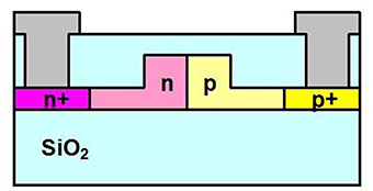
Figure 1. Diagram showing the cross section of the silicon optical phase modulator with PN junction positioned in the center of the waveguide. Lower SiO2 layer is 2 μm thick. Silicon overlayer is 220 nm thick, with slabs etched to a thickness of 100 nm to form the rib waveguide. The top SiO2 layer is 1 μm thick. Finally the electrodes are approximately 1.3 μm thick.
The fabrication process flow is almost identical to that used for the device with self-aligned PN junction. Firstly, the grating couplers are etched to a depth of 70 nm into the wafer surface using deep ultraviolet (DUV) lithography and dry etching. The active areas of the wafer are then implanted with boron to form the p-type regions. A silicon dioxide layer is then deposited onto the wafer and patterned with the waveguide design. This layer acts as a hard mask through which to etch the rib waveguides into the silicon overlayer. In the case of the self-aligned modulator this layer is retained and used in combination with a photoresist window to guide the phosphorus implantation which forms the n type regions. In this case the hard mask is stripped prior to the definition of the n-type implantation windows and the edge of implantation window is aligned to the center of the waveguide. The phosphorus implantation recipe is also adjusted in order to dope through the entire thickness of the silicon overlayer. The levels of doping in the p- and n-type regions are also adjusted such that depletion extends more evenly in terms of distance into the p- and n-type sections. Following this step further DUV lithography and ion implantation steps are used to define the highly doped p- and n- type regions. A rapid thermal annealing process is then employed to electrically activate the implanted dopants followed by the deposition of a 1 μm thick top silicon dioxide cladding layer. Contact holes are then etched through this layer down to the highly doped regions and the electrode metal deposited. Finally the coplanar waveguide electrode design is etched into this metal layer.
Results
The devices were tested by coupling light from a tunable laser to the fabricated samples using the surface grating couplers. Light was collected from the output side of the device again using a surface grating coupler and passed to a photo detector. Characterization of the DC performance was carried out by scanning the wavelength of the tunable laser around 1.55 μm and observing the transmission of the MZI with difference reverse bias voltages applied to the phase modulator in one arm. This transmission was then normalized to that of an undoped waveguide of the same length in order to estimate the on chip insertion loss of the modulator. Figure 2 shows the normalized spectral response of a device with 1 mm long phase shifters with 0, 3, 6, and 9 V applied. The static extinction ratio of the MZI structure is approximately 35 dB. The peak of the transmission is at approximately 5 dB. The optical loss of the MMI structures has been previously characterized to be approximately 0.5 dB [12]. The loss of the phase modulator is therefore estimated to be around 4 dB/mm which is slightly higher than that observed for the self-aligned modulator. The majority of this loss is expected to be due to the underestimation of the diffusion of dopants from the highly doped regions toward the waveguide during the annealing process [10], and therefore a much lower loss can be expected if this is simply compensated for in the design. Figures 3, 4 show the phase shift achieved from a 1 mm long phase shifter with reverse bias levels from 0 to 10 V applied and the modulation efficiency calculated at each point respectively. The results obtained from a self-aligned modulator are also plotted for comparison in Figures 3, 4. An improvement in efficiency is clearly visible with the junction positioned in the center of the waveguide.
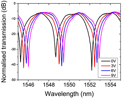
Figure 2. Normalized transmission spectra from a Mach-Zehnder device with 1 mm phase modulators with 0, 3, 6, and 9 V reverse bias voltages applied.
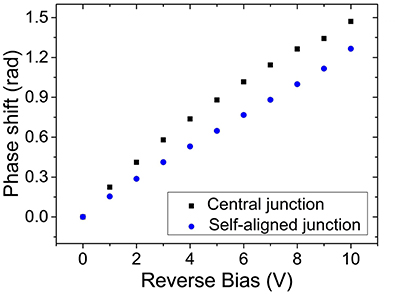
Figure 3. Phase shift vs. reverse bias voltage for 1 mm long central junction and self-aligned junction devices.
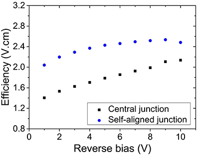
Figure 4. Modulation efficiency vs. reverse bias voltage for the central junction and self-aligned junction devices.
High speed testing was performed by applying an electrical pseudo random bit sequence (PRBS) data stream amplified to 6.5 V peak to peak. A bias tee was used to add a DC level to this drive signal in order to ensure that the device is operated in the reverse bias regime. High speed ground-signal-ground probes are used to apply both high speed and DC electrical signals to the input port of the coplanar waveguide electrodes and also to connect a DC block and 50 Ohm termination to the output port. The coplanar waveguide electrodes are widened at the ends to a pitch of 100 μm to accommodate probing. Output light from the device was amplified using an erbium doped fiber amplifier and filtered to remove amplified spontaneous emission noise from surrounding wavelengths to some extent before being measured using a digital communications analyser. Figure 5 shows the optical eye diagram obtained from a device with 1 mm phase modulators at 25 Gbit/s. The inset of the Figure 5 shows the electrical input eye to the device. The modulation depth is measured to be approximately 7 dB. Figure 6 shows an eye diagram obtained from a device with 500 μm long phase modulators at 52 Gbit/s. The modulation depth is estimated to be approximately 2 dB when residual noise from the 1 and 0 data levels is subtracted.
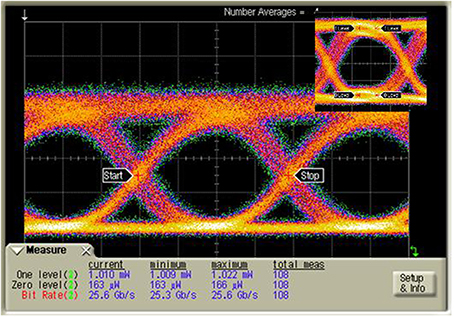
Figure 5. Optical eye diagram obtained from a device with 1 mm phase modulators at 25 Gbit/s.
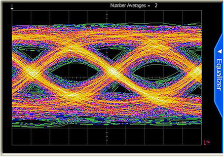
Figure 6. Optical eye diagram obtained from a device with 0.5 mm phase modulators at 52 Gbit/s.
Discussion
In the previous section, we demonstrated an improved modulation performance from a device with PN junction positioned in the center of the waveguide as compared to a self-aligned modulator which had the junction aligned with the edge of the waveguide rib. The formation of this device relied on the accuracy of a DUV lithographic process to align the PN junction in the center of the waveguide. Alignment errors are inherent in any lithography method to some extent and as a result it is not possible to be certain where the exact position of the PN junction is from device to device. Variations in the overlap between the optical mode and the region of depleted carriers will therefore occur which in turn cause device performance variations. Ideally, therefore a device with junction within the waveguide rib can be produced similar to that presented in this paper but with its PN junction formed by a self-aligned fabrication process. One method to do this is similar to what we presented previously [10, 11] and is depicted in Figure 7. Usually the ion implantation step which is self-aligned is performed with the ions at normal incidence to the wafer surface. One possibility is to position the wafer at an angle to the ion beam such that both the slab region and the sidewall of the waveguide rib are implanted. By varying the energy of the ions the distance which the ions penetrate into the waveguide can be varied and therefore the position of the junction inside the waveguide can be tailored as required. This approach can work well for Mach-Zehnder based modulators where the phase modulators are straight and the junction can be produced by tilting the wafer in one direction. Ring resonator based optical modulators are however more problematic as tilting the wafer in one direction will not allow the ions to penetrate into the waveguide rib around the entire circumference of the ring. An alternative approach is to use a technique which is not directional for example diffusion doping which will dope any area of the wafer which is not protected by a masking layer.
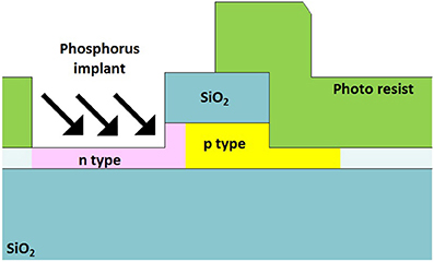
Figure 7. Adjusted self-aligned process to allow doping within the waveguide rib.
Summary
In this paper, we have presented experimental data from a PN junction based silicon Mach Zehnder modulator. Modulation efficiencies in the range 1.4 to 1.9 V/cm have been measured for reverse bias voltages between 0 V and 6 V. The on chip optical insertion loss for a 1 mm device has been measured to be 5 dB comprising 1 dB loss from the MMI splitter and combiner and 4 dB from the phase modulator. High speed modulation has been demonstrated in the form of eye diagrams up to a data rate of 52 Gbit/s. The performance of this device has also been compared to a device which had its PN junction self-aligned to the edge of the waveguide rib. An improvement in the modulation efficiency is demonstrated whilst the optical loss and high speed performance were approximately the same. Finally, we have discussed methods in which a device with PN junction within the waveguide rib can be produced using a self-aligned process.
Conflict of Interest Statement
The authors declare that the research was conducted in the absence of any commercial or financial relationships that could be construed as a potential conflict of interest.
Acknowledgments
The authors acknowledge funding in the European project HELIOS (FP7-224312) and by an EPSRC funded project in the UK, “Silicon Photonics for Future Systems.”
References
1. Paniccia M. Revolutionizing computing and communications with silicon photonics. IEEE Conf Group IV Photon (2014) 2014. [Oral Presentation].
2. Liu M, Yin X, Zhang X. Double-layer graphene optical modulator. Nano Lett. (2012) 12:1482–85. doi: 10.1021/nl204202k
Pubmed Abstract | Pubmed Full Text | CrossRef Full Text | Google Scholar
3. Feng D, Liao S, Liang H, Fong J, Bijlani B, Shafiiha R, et al. High speed GeSi electro-absorption modulator at 1550 nm wavelength on SOI waveguide. Opt Exp. (2012) 20:22224–32. doi: 10.1364/OE.20.022224
Pubmed Abstract | Pubmed Full Text | CrossRef Full Text | Google Scholar
4. Palmer R, Koeber S, Elder DL, Woessner M, Korn D, Lauermann M, et al. High-speed, low drive-voltage silicon-organic hybrid modulator based on a binary-chromophore electro-optic material. IEEE J Lightwave Technol (2014) 32:2726–34. doi: 10.1109/JLT.2014.2321498
5. Tang Y, Peters JD, Bowers JE. Over 67 GHz bandwidth hybrid silicon electroabsorption modulator with asymmetric segmented electrode for 1.3 μm transmission. Opt Exp (2012) 20:11529–35. doi: 10.1364/OE.20.011529
Pubmed Abstract | Pubmed Full Text | CrossRef Full Text | Google Scholar
6. Bourdais LE, Cassan E, Marris-Morini D, Izard N, Maroutain T, Maillard F, et al. Pockels effect study in Strained Silicon Mach-Zenhder Interferometer. IEEE Conf Group IV Photon (2014) 2014:243–4. doi: 10.1109/Group4.2014.6961945
7. Nedeljkovic M, Soref R, Mashanovich GZ. Free-carrier electro-refraction and electro-absorption modulation predictions for silicon over the 1-14 um wavelength range. IEEE J Photon (2011) 3:1171–80. doi: 10.1109/JPHOT.2011.2171930
8. Reed GT, Mashanovich GZ, Gardes FY, Nedeljkovic M, Thomson DJ, Ke L, et al. Recent breakthroughs in carrier depletion based silicon optical modulators. Nanophotonics (2013) 3:229–45. doi: 10.1515/nanoph-2013-0016
9. Webster M, Gothoskar P, Patel V, Piede D, Anderson S, Tummidi R, et al. An efficient MOS-capacitor based silicon modulator and CMOS drivers for optical transmitters. IEEE Conf Group IV Photon (2014) 2014:1–2. doi: 10.1109/Group4.2014.6961998
10. Thomson DJ, Gardes FY, Liu S, Porte H, Zimmermann L, Fedeli J-M, et al. High performance mach zehnder based silicon optical modulators. IEEE J Sel Top Quant Electron (2013) 19:3400510. doi: 10.1109/JSTQE.2013.2264799
11. Gardes FY, Thomson DJ, Emerson NG, Reed GT. 40 Gb/s silicon photonics modulator for TE and TM polarisations. Opt Exp (2011) 19:11804–14. doi: 10.1364/OE.19.011804
Pubmed Abstract | Pubmed Full Text | CrossRef Full Text | Google Scholar
Keywords: 52 Gb/s, electro-optic modulator, silicon photonics, Mach-Zehnder, carrier depletion
Citation: Reed GT, Thomson DJ, Gardes FY, Hu Y, Fedeli J-M and Mashanovich GZ (2014) High-speed carrier-depletion silicon Mach-Zehnder optical modulators with lateral PN junctions. Front. Phys. 2:77. doi: 10.3389/fphy.2014.00077
Received: 07 October 2014; Accepted: 28 November 2014;
Published online: 16 December 2014.
Edited by:
Ching Eng Jason Png, Optic2Connect Pte Ltd, SingaporeReviewed by:
Francisco Welington Lima, Universidade Federal do Piauí, BrazilSultan Akhtar, GC University Lahore, Pakistan
Copyright © 2014 Reed, Thomson, Gardes, Hu, Fedeli and Mashanovich. This is an open-access article distributed under the terms of the Creative Commons Attribution License (CC BY). The use, distribution or reproduction in other forums is permitted, provided the original author(s) or licensor are credited and that the original publication in this journal is cited, in accordance with accepted academic practice. No use, distribution or reproduction is permitted which does not comply with these terms.
*Correspondence: Graham T. Reed, Optoelectronic Research Centre, University of Southampton, Mountbatten Building, Highfield, Southampton, Hampshire SO17 1BJ, UK e-mail: g.reed@soton.ac.uk