Silicon optical modulator simulation
 Soon Thor Lim
 Min Jie Sun2
  Ching Eng Png
- 1Institute of High Performance Computing, Agency of Science, Technology and Research, Singapore, Singapore
- 2OPTIC2connect, Singapore, Singapore
We developed a way of predicting and analyzing high speed optical modulator. Our research adopted a bottom-up approach to consider high-speed optical links using an eye diagram. Our method leverages on modular “mapping” of electrical characteristics to optical characteristics, while attaining the required accuracy necessary for device footprint approaching sub-micron scales where electrical data distribution varies drastically. We calculate for the bias dependent phase shift and loss for the optical modulator based on the real and imaginary part of complex effective indices. Subsequently, combine effectively both the electrical and optical profiles to construct the optical eye diagram which is the essential gist of signal integrity of such devices.
Introduction
Datacenter infrastructure has been one of the fastest growing areas for IT networking driven by ever-increasing need for a higher and faster number of connections between servers and switches. One of the characteristics of datacenters is the need for low cost, high performance, high density, and low power connection. The size, power dissipation, and cost structure of today's coherent transceivers, which were developed for long-haul applications, limit these modules' application in the more cost-sensitive environment where space comes at a high premium, making line-card density very important. Consequently, a path to a lower-cost coherent module in a smaller footprint has become increasingly important.
Silicon photonics could potentially play an important role in delivering these requirements. The potential disruption of silicon photonics lies in high-speed transmission of 40G and 100G in two MSA (Multi-source agreement) form-factor families. One of the challenges is to realize silicon optical modulator, which is a key device for data transmission. Plasma dispersion effect is the most common method used in silicon optical modulator. The real and imaginary parts of the refractive index change with the concentration of free carriers. The change in the real and imaginary parts of the refractive index has been evaluated qualitatively at telecommunication wavelength of 1.55 μm [1]. There are several common approaches to manipulate the charge density for silicon, such as carrier injection, accumulation and depletion. Our modeling and simulation focused on depletion type of silicon modulators due to its insensitive to carrier lifetime, thus greater potential for high speed application. Several carrier depletion based modulators with data transmission in excess of tens of Giga-bit-per-second have been proposed [2–15].
Conventional method to study the optical modulator uses two different models. Firstly, is to investigate the electrical behavior and after which the modulator is simulated from an optical point of view taking into account the electrically induced silicon refractive index change. At the best of our knowledge, these two models have been developed in two different simulation environments, the former purely electrical [16] and the latter purely optical [17], giving some consequent problems and inaccuracies in using the electrical simulation results in the environment where optical simulation is performed.
Recognizing these simulation challenges, and vital role of such modulator, the team focused our research efforts in studying these modulators specifically. We performed and developed a modeling and simulation suite for optical modulator, which aims to overcome these problems. We make predictions of key optical signal fidelity and model optical modulator in conjunction with industrialists based on a careful analysis of experimental data reported in the literature.
Modulator Structure for Modeling and Simulation
Two state-of-the-art high speed depletion based silicon modulator structure are used to illustrate the methods and results of our high speed simulation. The first modulator design was published by Thomson et al. [15] in 2011 and the second modulator design was revised by Liow et al. [11] in 2010.
The cross-section of the first modulator is shown in Figure 1A and shall be referred as mod1. Mod1 modulator is formed by p-type silicon at the rib region extending toward one side of the slab region, while the other side of the slab region is formed by n-type silicon. The p+ and n+ are highly doped regions to form ohmic contacts which connect p and n regions with the coplanar waveguide electrodes. The latter is referred as mod2 with its cross-section as shown in Figure 1B. For Mod2 structure, the p-n junction is located slightly toward the right of the rib waveguide to maximize optical mode interaction with the carrier depletion movement. Highly doped p+ and n+ regions are placed 600 nm away from the p-n junction to minimize excessive absorption loss. Coplanar waveguides are connected to the p+ and n+ region through Aluminium electrodes. Both modulators are based on lateral p-n junction fabricated in a Mach-Zehnder interferometer (MZI) configuration.
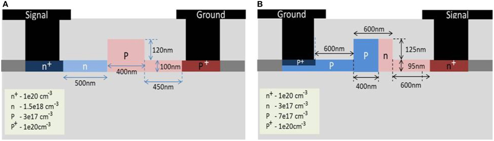
Figure 1. Diagrams showing depletion based silicon modulator based lateral p-n junction fabricated in a Mach-Zehnder interferometer (MZI) configuration. (A) mod1 and (B) mod2.
Modulator Simulation
Optical modulation can be achieved by arranging silicon phase shifters in Mach-Zehnder Interferometer or ring resonator configurations. Performance of these silicon phase shifters determines performance of the overall modulating speed and efficiency. Phase shifting efficiency and loss are two important parameters to gage the performance of a silicon phase shifter. Both semiconductor device and optical simulations are required to simulate the efficiency and loss of a silicon phase shifter. In this work, we used SILVACO [16] Atlas device simulator to perform device simulation. It solves the Poisson's Equation and the Carrier Continuity Equations in thermal equilibrium and calculates electron and hole distributions at various doping concentration levels under different biasing conditions. In the simulation, carrier statistics are assumed to be Fermi-Dirac, carrier mobility are assumed to be doping concentration dependent and Klaassen's model [18, 19] is also applied. A DC Voltage was swept from 0 to −10V in device anode with 1V step. Carrier distributions at each reverse bias point were calculated. Plasma dispersion effect [1] describes complex refractive indices change with carrier concentration in silicon. According to the governing equations of plasma dispersion [1], carrier concentrations are transformed to change in refractive indices at each reverse bias point from 0 to −10V. The transformed data were input into a finite difference optical solver to calculate effective refractive indices.
The main challenges in optical modulator modeling and simulation exist in dealing with different physical domain that requires different set of governing physics equations, i.e., drift-diffusion model for semiconductor physics [20] and beam propagation method (BPM) [21–24] for optical field propagation. The simulator does not provide a prediction of the overlap integral between the electrical carriers and the optical field. Therefore, it will be shown that there exists a high degree of non-uniformity in the predicted injected carrier concentration at the levels of interests throughout the central guiding region of the device footprint approaching sub-micron (220 nm overlayer) scales where electrical data distribution varies drastically. This is clearly shown in Figures 2, 3 the contour plots of the carrier's concentration and the equivalent complex refractive indices. It can be noted that the distribution of electrons and holes in the sub-micron rib waveguiding region is non-uniformly distributed. If we obtained from SILVACO the mean value of the injected carrier concentration in the guiding region as demonstrated in large device > 1 μm overlayer [25], it will yield a high degree of inaccuracy. Hence, to obtain the resulting changes in refractive index and absorption for the device under investigation, the data from the electrical simulation need to be mapped into a similar grid-based optical simulator to predict absorption and refractive-index changes.
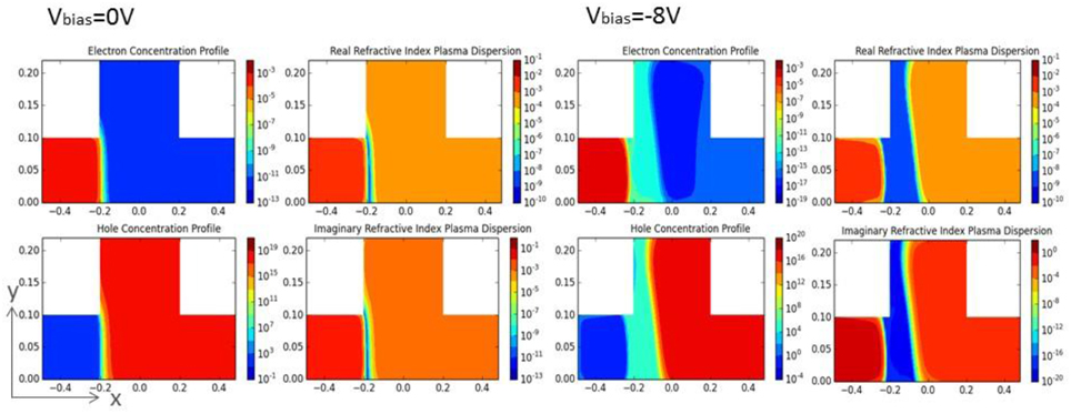
Figure 2. Contour plots of non-uniform carrier concentration and it equivalent complex refractive indices for mod1 at 0V and −8V.
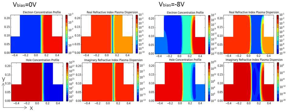
Figure 3. Contour plots of non-uniform carrier concentration and it equivalent complex refractive indices for mod2 mod1 at 0V and −8V.
Our technique is able to perform modular “mapping” of complex optical waveguide structure either in 2 dimensions or 3 dimensions [26, 27], where device footprints are in the order of hundreds of nanometers. In the case of mod1 and mod2 device structure, the small variation of non-uniformity within the waveguide core can have significant change in device performance. Hence, cross-sectional cutline method to evaluate the device performance will not be accurate. Therefore, we employed “modular mapping” as shown in Figures 2, 3 that allows us to map over 10,000 data points in a cross-sectional area of 220 nm waveguide as compared to tens of data points in conventional modeling.
Propagation constants of the waveguide across various voltage bias points were calculated using finite difference method. Semi-vector and full-vector description of this method can be found in numerous literatures [28–30]. Our implementation take into consideration the eigenmodes and propagation constants of the waveguide calculated using Scipy eigs function [31], which is based on the implicitly restarted Arnoldi method [32]. The optical solver discretize the Wave Equation, forms a sparse matrix and solves the eigenvalue to obtain the fundamental mode profile and the effective indices. The optical mode profile for mod1 and mod2 are shown in Figure 4 together with the carrier concentration at reverse bias of 8V. Resulted effective indices are dependent on the carrier distributions at different reverse bias. Phase difference between two voltages is calculated by:
L is phase shifter length. λ is wavelength. Δneff = nR, V1−nR, V2 is the difference of real effective index between voltage bias V1 and V2. Phase shifting efficiency is defined by Δϕ/ΔV where ΔV voltage difference. Absorption loss was calculated by the imaginary refractive index at each reverse bias voltage:
For complex device structure, the imaginary-distance beam propagation method [33] for eigenmode calculation can be used. In this case, both methods are used to analyze both mod1 and mod2 and the give very similar results and agrees well with [11, 15, 34] which verifies that our implementation is correct. For clarity, results obtained from finite difference method are discussed.
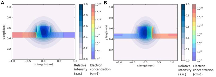
Figure 4. Optical mode profile overlaps with electrical domain (A) mod1 and (B) mod2.
Figure 5 shows the bias dependent phase shift (2π /mm) and loss (dB/mm) for mod1 and mod2 which can be calculated from the real and imaginary part of complex effective index respectively. The applied bias varies from 0V to −8V, i.e., reverse bias, which depletes the carriers from the junction of p-doped and n-doped regions. Δneff increases with the increasing reverse bias, hence induced higher phase changes due to carrier depletion in the rib region. On the other hand, reduction in carriers decreases the carrier induced absorption of the light. Therefore, as expected, losses decrease with an increase in the reverse bias voltage. It can also be noted that mod2 has a better phase shift efficiency as shown in Figure 5. This is probably due to the depletion region formed closer to the center of the waveguide, allowing greater interaction between the optical mode and the depletion region. A drawback of this is that it also allows more interaction between the optical mode and the n-type region. This will create more loss as evidenced by the comparison of attenuation coefficient per mm between mod1 and mod 2 as shown in Figure 5.
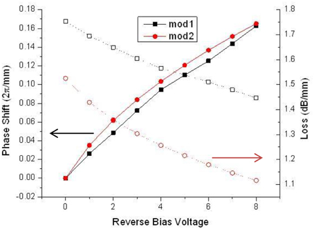
Figure 5. Phase shift efficiencies and loss for mod1 and mod2.
High Speed Eye Diagram Simulation
Silicon phase shifters are usually applied to ring resonators or Mach-Zehnder (MZ) interferometer structures to achieve On-Off-Keying (OOK). Eye diagram is generated at the output of an OOK communication system to measure the performance of the system. System with bigger eye opening, which is quantified by the extinction ratio, has better bit-error-rate performance at certain noise level. In this work, eye diagram is generated by simulating the behavior of a single drive Mach-Zehnder Modulator (MZM) with random bit sequence. Our simulated eye diagram at 10-Gb/s NRZ OOK has demonstrated and verified against experimental data [34] with good agreement.
The length of MZM was set to be 3.5 mm in simulation model. Effect of imbalance arms was modeled by phase difference at the output. Phase shifter in one arm of the MZM was biased with 4V reverse DC bias and 4V peak-to-peak RF signal, which was generated by a random 40Gbps bit sequence. Calculated eye diagram is shown in Figure 6A, compared to Figure 6B, measured eye diagram in Thomson et al. [15]. Extinction ratio (ER) of the simulated eye diagram is 7.3 dB, calculated with 10log10 ((1 power level)/(0 power level)). The simulated ER closely matches the measured 7 dB ER [15].
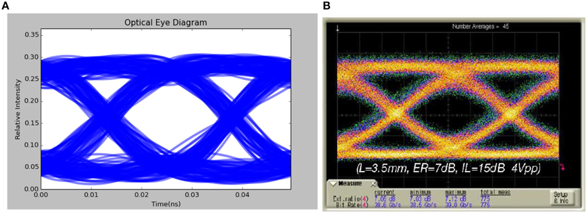
Figure 6. (A) Mod1 Eye diagram simulated with 3.5 mm MZM, 40 Gbps 4V peak-to-peak RF signal input. (B) Eye diagram derived from optical PRBS data output at 40 Gbit/s. 3.5 mm MZI with 4V RF signal operated at quadrature (7 dB ER).
Conclusions
Our research adopted a bottom-up approach to consider high-speed optical links using an eye diagram. We perform modular “mapping” in a non-uniform distributed electron and holes carrier's concentration for sub-micron rib waveguiding region. The data from the electrical simulation is mapped into a similar grid-based optical simulator to predict absorption and refractive-index changes. This is to solve for the real and imaginary part of complex effective indices, which are used to calculate for the bias dependent phase shift (2π /mm) and loss (dB/mm) for the optical modulator respectively. This predictive approach is exemplified by the analysis of the modulation of the optical signal with best-in-class depletion-based silicon modulators arranged in a Mach-Zehnder Interferometer (MZI) configuration. The simulated silicon phase shifter efficiency and eye diagram closely matched experimental measurements.
Conflict of Interest Statement
The authors declare that the research was conducted in the absence of any commercial or financial relationships that could be construed as a potential conflict of interest.
References
1. Soref RA, Bennett BR. Electrooptical effects in silicon. IEEE J Q Electron. (1987) Vol. QE-23, No. 1. doi: 10.1109/JQE.1987.1073206
2. Gardes FY, Reed GT, Emerson NG, Png CE. A sub-micron depletion-type photonic modulator in silicon on insulator. Opt Express (2005) 13:8845–54. doi: 10.1364/OPEX.13.008845
PubMed Abstract | Full Text | CrossRef Full Text | Google Scholar
3. Marris-Morini D, Le Roux X, Vivien L, Cassan E, Pascal D, Halbwax M, et al. Optical modulation by carrier depletion in a silicon PIN diode. Opt Express (2006) 14:10838–43. doi: 10.1364/OE.14.010838
PubMed Abstract | Full Text | CrossRef Full Text | Google Scholar
4. Liao L, Liu A, Rubin D, Basak J, Chetrit Y, Nguyen H, et al. 40 Gbit/s silicon optical modulator for high speed applications. Electron Lett. (2007) 43:1196–7. doi: 10.1049/el:20072253
5. Liu A, Liao L, Rubin D, Nguyen H, Ciftcioglu B, Chetrit Y, et al. High-speed optical modulation based on carrier depletion in a silicon waveguide. Opt Express (2007) 15:660–8. doi: 10.1364/OE.15.000660
PubMed Abstract | Full Text | CrossRef Full Text | Google Scholar
6. Marris-Morini D, Vivien L, Fédéli JM, Cassan E, Lyan P, Laval S. Low loss and high speed silicon optical modulator based on a lateral carrier depletion structure. Opt Express (2008) 16:334–9. doi: 10.1364/OE.16.000334
PubMed Abstract | Full Text | CrossRef Full Text | Google Scholar
7. Spector SJ, Geis MW, Zhou G-R, Grein ME, Gan F, Popovic MA, et al. CMOS-compatible dual-output silicon modulator for analog signal processing. Opt Express (2008) 16:11027–31. doi: 10.1364/OE.16.011027
PubMed Abstract | Full Text | CrossRef Full Text | Google Scholar
8. Gill DM, Patel SS, Rasras M, Tu K-Y, White AE, Chen Y-K, et al. CMOS compatible Si-ring assisted Mach-Zehnder interferometer with internal bandwidth equalization. In: Proceedings of 6th IEEE International Conference on Group IV Photonics. San Francisco, CA: IEEE (2009).
9. Dong P, Liao S, Feng D, Liang H, Zheng D, Shafiiha R, et al. Low Vpp, ultralow-energy, compact, high-speed silicon electro-optic modulator. Opt Express (2009) 17:22484–90. doi: 10.1364/OE.17.022484
PubMed Abstract | Full Text | CrossRef Full Text | Google Scholar
10. Feng NN, Liao S, Feng D, Dong P, Zheng D, Liang H, et al. High speed carrier-depletion modulators with 1.4V-cm VπL integrated on 0.25μm silicon-on insulator waveguides. Opt Express (2010) 18:7994. doi: 10.1364/OE.18.007994
PubMed Abstract | Full Text | CrossRef Full Text | Google Scholar
11. Liow T-Y, Ang K-W, Fang Q, Song J-F, Xiong Y-Z, et al. Silicon Modulators and Germanium Photodetectors on SOI: Monolithic Integration, Compatibility, and Performance Optimization. In: Selected Topics in Quantum Electronics, IEEE Journal of Vol. 16, Issue 1, IEEE (2009) pp. 307–315. doi: 10.1109/JSTQE.2009.2028657
12. Xin M, Png CE, Danner AJ. Breakdown delay-based depletion mode silicon modulator with photonic hybrid-lattice resonator. Opt Express (2011) 19:5063–76. doi: 10.1364/OE.19.005063
PubMed Abstract | Full Text | CrossRef Full Text | Google Scholar
13. Xin M, Png CE, Lim ST, Dixit V, Danner AJ. A high speed electro-optic phase shifter based on a polymer-infiltrated P-S-N diode capacitor. Opt Express (2011) 19:14354–69. doi: 10.1364/OE.19.014354
PubMed Abstract | Full Text | CrossRef Full Text | Google Scholar
14. Gardes FY, Thomson DJ, Emerson NG, Reed GT. 40 Gb/s silicon photonics modulator for TE and TM polarisations. Opt Express (2011) 19:11804–14. doi: 10.1364/OE.19.011804
PubMed Abstract | Full Text | CrossRef Full Text | Google Scholar
15. Thomson DJ, Gardes FY, Hu Y, Mashanovich G, Fournier M, Grosse P, et al. High contrast 40Gbit/s optical modulation in silicon. Opt Express (2011) 19:11507–16. doi: 10.1364/OE.19.011507
PubMed Abstract | Full Text | CrossRef Full Text | Google Scholar
18. Klaassen DBM. A unified mobility model for device simulation- I. model equations and concentration dependence. Solid-State Elect. (1992) 35:953–9. doi: 10.1016/0038-1101(92)90325-7
19. Klaassen DBM. A unified mobility model for device simulation - II. temperature dependence of carrier mobility and lifetime. Solid-State Elect. (1992) 35:961–7. doi: 10.1016/0038-1101(92)90326-8
21. Scarmozzino R, Gopinath A, Pregla R, Helfert S. Numerical techniques for modeling guided-wave photonic devices. J Select Top Quant Electron. (2000) 6:150. doi: 10.1109/2944.826883
22. Scarmozzino R, Osgood Jr RM. Comparison of finite-difference and Fourier-transform solutions of the parabolic wave equation with emphasis on integrated-optics applications. J Opt Soc Am A (1991) 8:724. doi: 10.1364/JOSAA.8.000724
23. Hadley GR. Transparent boundary condition for the beam propagation method. Opt Lett. (1991) 16:624. doi: 10.1364/OL.16.000624
PubMed Abstract | Full Text | CrossRef Full Text | Google Scholar
24. Hadley GR. Transparent boundary condition for the beam propagation method. J Quant Electron. (1992) 28:363. doi: 10.1109/3.119536
25. Png CE, Chan SP, Lim ST, Reed GT. Optical phase modulators for MHz and GHz modulation in silicon-on-insulator (SOI). J Lightwave Tech. (2004) 22:1573–82. doi: 10.1109/JLT.2004.827655
26. Dixit V, Png CE, Lim ST. Multi Physics, Multi Domain Adaptive Mapping of Optical Devices, IHPC Proprietary know-how. Singapore (2012).
27. Stern MS. Semivectorial polarised finite difference method for optical waveguides with arbitrary index profiles. Optoelectron IEE Proc J. (1998) 135:56, 63. doi: 10.1049/ip-j.1988.0013
28. Vassallo C. Improvement of finite difference methods for step-index optical waveguides. Optoelectron IEE Proc J. (1992) 139:137, 142.
29. Xu CL, Huang W-P, Stern MS, Chaudhuri SK. Full-vectorial mode calculations by finite difference method. Optoelectron IEE Proc. (1994) 141:281, 286. doi: 10.1049/ip-opt:19941419
30. Fallahkhair AB, Li KS, Murphy TE. Vector finite difference modesolver for anisotropic dielectric waveguides. J Lightw Technol. (2008) 26:1423–31. doi: 10.1109/JLT.2008.923643
32. Lehoucq RB, Sorensen DC, Yang C. ARPACK USERS GUIDE: Solution of Large Scale Eigenvalue Problems by Implicitly Restarted Arnoldi Methods. Philadelphia, PA: SIAM (1998).
33. Jungling S, Chen JC. A study and optimization of eigenmode calculations using the imaginary-distance beam-propagation method. IEEE J Quant Electron. (1994) 30:2098, 2105.
Keywords: silicon photonics, optical modulator, high speed simulation, eye diagram
Citation: Lim ST, Sun MJ and Png CE (2015) Silicon optical modulator simulation. Front. Phys. 3:27. doi: 10.3389/fphy.2015.00027
Received: 27 January 2015; Paper pending published: 20 February 2015;
Accepted: 30 March 2015; Published: 21 April 2015.
Edited by:
David John Thomson, University of Southampton, UKReviewed by:
Joan J. Carvajal Marti, Universitat Rovira i Virgili, SpainAllbens Picardi Faria Atman, Centro Federal de Educação Tecnológica de Minas Gerais - CEFET/MG, Brazil
Copyright © 2015 Lim, Sun and Png. This is an open-access article distributed under the terms of the Creative Commons Attribution License (CC BY). The use, distribution or reproduction in other forums is permitted, provided the original author(s) or licensor are credited and that the original publication in this journal is cited, in accordance with accepted academic practice. No use, distribution or reproduction is permitted which does not comply with these terms.
*Correspondence: Soon Thor Lim, Institute of High Performance Computing, Agency of Science, Technology and Research, 1 Fusionopolis Way, #16-16 Connexis, Singapore, Singapore limst@ihpc.a-star.edu.sg