Spin injection in indium arsenide
 Mark Johnson
 Hyun Cheol Koo
 Suk Hee Han2
  Joonyeon Chang
- 1US Naval Research Laboratory, Washington, DC, USA
- 2Center for Spintronics, Korean Institute of Science and Technology, Seoul, South Korea
In a two dimensional electron system (2DES), coherent spin precession of a ballistic spin polarized current, controlled by the Rashba spin orbit interaction, is a remarkable phenomenon that's been observed only recently. Datta and Das predicted this precession would manifest as an oscillation in the source-drain conductance of the channel in a spin-injected field effect transistor (Spin FET). The indium arsenide single quantum well materials system has proven to be ideal for experimental confirmation. The 2DES carriers have high mobility, low sheet resistance, and high spin orbit interaction. Techniques for electrical injection and detection of spin polarized carriers were developed over the last two decades. Adapting the proposed Spin FET to the Johnson–Silsbee non-local geometry was a key to the first experimental demonstration of gate voltage controlled coherent spin precession. More recently, a new technique measured the oscillation as a function of channel length. This article gives an overview of the experimental phenomenology of the spin injection technique. We then review details of the application of the technique to InAs single quantum well (SQW) devices. The effective magnetic field associated with Rashba spin-orbit coupling is described, and a heuristic model of coherent spin precession is presented. The two successful empirical demonstrations of the Datta Das conductance oscillation are then described and discussed.
1. Introduction
The transport of spin polarized carriers in conductors has been a large and highly active research field for the last four decades. Seminal work included many contributions: a theoretical framework that described spin polarized electric currents in ferromagnets [1]; experimental studies of spin polarized electric current that tunnels from a ferromagnet, across a thin insulating tunnel barrier and into a thin superconducting film [2]; the introduction of the magnetic tunnel junction (MTJ), a ferromagnet/insulator/ferromagnet sandwich structure (F1/I/F2) [3]; and, later, the discovery of the Giant Magnetoresistance and spin valve effects [4, 5]. The experiments described in this article developed from the spin injection approach.
In the mid-1980s, the spin injection technique introduced a ferromagnet/nonmagnetic conductor/ferromagnet lateral structure (F1/N/F2) [6, 7] that was derived conceptually from transmission electron spin resonance (TESR). A series of experiments demonstrated that spin polarized electric current JM could be driven from F1 into N, where a nonequilibrium population of spin polarized carriers, equivalently called a spin accumulation , would develop if the spin relaxation time τs, n was sufficiently long. This spin population diffused away from the injecting source and the diffusion current was recognized as a pure spin current JM, n. The characteristic diffusion length, often called λs, is identically the same as the spin diffusion length defined in TESR, , where D is the electron diffusion constant.
Using a model converse to that for interfacial spin injection, the second electrode F2 could be used to detect the spin accumulation as a voltage Vs or equivalently, resistance Rs. The F1/N/F2 structure became known as the nonlocal lateral spin valve and its details are described with the aid of Figure 1. The injector and detector are thin, narrow electrodes that span the width of the sample. Bias current I is injected uniformly along F1 and the dotted lines represent equipotentials that describe the linear voltage drop from injector to ground. The sample region x > 0 is equipotential because the net current flow in this region is zero and therefore no voltage drop exists. However, the spin accumulation diffuses equally along the ±x−axis (gray shading in Figure 1). The magnitude of decreases exponentially . The magnitude of Rs in the vicinity of the detector can be determined from magnetoresistance measurements using an in-plane magnetic field, Hy. Electrodes F1 and F2 have easy magnetization axes along ŷ, and are fabricated to have square hysteresis loops with different values of switching fields. The resistance measured at the detector is high when magnetizations M1 and M2 are parallel, but a resistance dip of magnitude ΔR = 2Rs is observed when M1 and M2 are antiparallel. Measurements of λs and τs are achieved by measuring Rs as a function of distance L between the injector and detector. Alternatively, a transverse magnetic field can be used to dephase the polarization of the nonequilibrium spins. The latter technique is a direct analog of TESR performed at zero frequency, called the Hanle effect, and is discussed in detail in Section 1.1. Theory for the spin injection phenomenology was derived using a microscopic transport model [8] and a more formal thermodynamic approach [9].
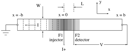
Figure 1. Geometry of the nonlocal lateral spin valve (NLSV), top view.
The study of spin polarized currents in semiconductors has been a highly important research topic for the last two decades. Shortly after the introduction of spin injection [6], Datta and Das proposed an idea for applying the technique to semiconductors. They proposed a field effect transistor (FET) structure in which the channel was a two dimensional electron gas (2DEG) in a compound III-V heterostructure. Ferromagnetic metal electrodes were used as source and drain (F1/2DEG/F2) and performed as spin injector and detector [10]. Their experiment proposed a demonstration of a remarkable property of a 2DEG that relied on Rashba spin orbit coupling. In Rashba's model, a spin orbit interaction arises when the confining potential of a 2DEG has a strong spatial asymmetry [11, 12]. Datta and Das predicted that a current of ballistic spin polarized electrons, injected at the source, would precess coherently during their ballistic trajectories along the channel and that the coherent spin phase could be detected as the spin-dependent current (or voltage) sensed by the detector at the drain. Furthermore, a gate voltage applied to the channel would modulate the Rashba coupling and cause a change in wavelength of the coherent spin precession. In this way, the channel conductance would oscillate as a function of gate voltage.
The proposed device became known as a spin injected field effect transistor, or Spin-FET, and became the focus of research in the field of spintronics. From the perspective of fundamental physics, the predicted conductance oscillation represented a novel phenomenon involving coherent spin phase and a unique manifestation of a relativistic effect in a solid state system. Interest in applications was equally high. The success of MTJs for applications as storage cells in integrated nonvolatile random access memory arrays and as sensors in hard disk drive read heads motivated applied research in all areas of spin transport. Control of spin polarized currents in semiconductors was believed to offer new avenues for device functionality because semiconductor devices already are the dominant device family for information processing. This article reviews the study of spin dependent transport in high mobility indium arsenide quantum wells. A focus will be a review of experiments that demonstrate operation of the Spin-FET and provide empirical observation of the Datta Das conductance oscillation.
1.1. Electron Spin Transport Techniques
In this section we review details of the spin injection technique. As introduced above, thin ferromagnetic film F1 injects spin polarized carriers in a conducting sample and film F2 acts conversely as a spin detector. Two methods that employ an external magnetic field can be used to measure spin accumulation. In the first, a field applied in the plane of the sample controls the magnetizations of injector and detector to be either parallel or antiparallel. In the second, a transverse magnetic field applies a torque on the spin magnetic moment of the injected carriers and two kinds of features can be observed in the data: (1) ballistic Larmor waves or (2) a diffusive Hanle effect. These features are common in transmission electron spin resonance which is briefly reviewed with the aid of Figure 2. In TESR, a thin foil sample divides a resonant cavity into two equal portions. Microwave photons are supplied to the “transmit” side, are absorbed within a skin depth of the foil, and create a nonequilibrium population of spin polarized electrons.
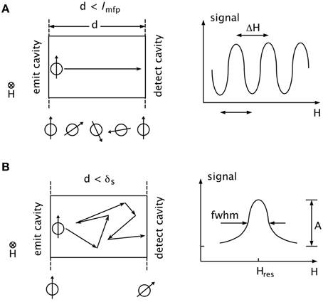
Figure 2. Schematic description of transmission electron spin resonance (TESR) in different transport regimes. Left panels: Cross section of metal foil samples having thickness d, with transmit cavity on left and detect cavity on right, and depiction of carrier transport. Right panels: qualitative sketch of detected resonance signals. (A) Carrier transport is ballistic. (B) Carrier transport is diffusive.
The nonequilibrium spins move by diffusion across the sample. On the opposite side, within a skin depth of the surface, spin flip processes generate inverse transitions and microwave photons are emitted into the “detect” cavity. The microwave frequency range that's commonly used is X-band, with frequency ν ≈ 10 GHz, (wavelength λ ≈ 3 cm). Experimentally, a fixed frequency is chosen and the magnetic field H is swept. The amplitude A of the transmitted microwave “signal” measured in the “detect” cavity varies with external field, A(H). For ν ≈ 10 GHz the resonant field is calculated from the free electron ratio ν∕H = 2.8 × 10⁶ Hz/Oe, and one finds Hres ≈ 3600 Oe. The maximum amplitude of the “signal” is centered at the resonant field and the shape of the function A(H) depends directly on the spin transport processes inside the foil sample. Examples are shown in the schematic drawings of Figure 2. The panels on the left depict a cross-section of a sample N of thickness d. The sample would be mounted between a transmit cavity on the left and a detect cavity on the right and field H is perpendicular to the sample plane. The panels on the right show the line shapes A(H) of resonant signals for two different conditions [13].
Successful observation of TESR requires using a sample N with a long spin relaxation time, T2, and therefore a low spin scattering rate, 1∕T2. A thin foil pressed from high purity bulk metal has very low resistivity and very long values of T2 at cryogenic temperature. In Figure 2A, the foil thickness d is less than the electron mean free path, d < ℓ, because the conductivity is high and ℓ is long. The spin-polarized electrons entering at the left boundary of the foil move at the Fermi velocity vF and have ballistic trajectories across the width of the foil. Throughout the sample, and particularly at the right boundary, a nonequilibrium population of “hot” electrons, with energies and wave vectors near the Fermi surface, have the same spin phase. When any ballistic electron scatters off the right boundary surface, that scattering event may flip the electron spin by π radians. With such an event, the nonequilibrium population diminishes and a microwave photon is emitted. For any value H of field, all the ballistic electrons reaching the other side have the same phase because there have been no scattering events and therefore nothing alters the phase. As the magnetic field is monotonically varied, the spin phase accumulated by each electron along the ballistic trajectory changes. A change of field ΔH corresponds to a spin phase change of 2π (Figure 2A). The spin phase of the nonequilibrium population at the right boundary will be spin up (down) when H, vF, and the length of the trajectory correspond to rotations of nπ, with n even (odd). The line shape A(H) detected by the “receive” cavity shows oscillations that repeat with undiminished amplitude. Spin precession occurs at the Larmor frequency and this phenomenon is called a Larmor wave [14].
In Figure 2B, the foil thickness is greater than ℓ but smaller than δs, ℓ < < d < δs. Nonequilibrium spin polarized electrons, , are induced at the left boundary of N. There is no “spin pumping” in the interior of N, and therefore there is a gradient of spin dependent electrochemical potential across the foil. This gradient drives self-diffusion of the spin-polarized electrons. All the diffusing conduction electrons begin, at the left boundary, with the same spin phase. They all acquire precessional phase angle, in magnetic field H, at the same rate. However, the diffusion process means that a few electrons move directly across the foil in just a few steps. The majority of carriers encounter numerous scattering events and have taken many steps by the time they reach the right boundary. At field H = Hres, the signal is maximum because all the electrons have the original phase (spin “up” in Figure 2B) when they reach the other side. As the difference |H − Hres| increases, the carriers that have taken many steps to cross the width have a large relative phase angle and the distribution of phase angle is proportional to the distribution of steps taken in the diffusion process. At large values of |H − Hres|, the distribution of phase is so large that spin orientation is random and the signal is zero. Spin scattering events impose a limit to the contribution of any electron to the signal. The result is a line shape, depicted in the right panel of Figure 2B, that is similar to a Lorentzian. Unlike a Lorentzian, the decay shape need not be monotonic but may develop shallow dips and wings. The half width at half maximum, in the “thin limit” with d < < δs, is Hhwhm = 1∕(γT2). This is a manifestation of the Hanle effect, the dephasing of a diffusive spin population under the influence of a transverse magnetic field [15].
1.2. Transverse Field Method using the Nonlocal Lateral Spin Valve
Spin injection and the NLSV were introduced in Section 1. An external field applied transverse to the orientation of injected carriers has been used to measure spin relaxation with the Hanle effect in N materials with low spin orbit interaction, including bulk metal [6], metal films [16, 17], n − doped silicon [18], and GaN nanowires [19]. When and are parallel and ℓ < < L < λs, a detector voltage measurement as a function of transverse magnetic field, Vd(Hz), shows a Hanle trace. Rigorous fits, found as solutions of the Bloch equations with a one dimensional diffusion term [8], differ slightly from a pure Lorentzian as noted above.
Larmor waves have not been observed in NLSV devices because the device regime L < ℓ has not been achieved. However, the concept of the nonlocal geometry also applies to a system with ballistic transport. Referring to Figure 1, carriers injected at x = 0 have a distribution of initial velocities with magnitude vF. Half the carriers have an x component, vF, x > 0. By constraining the geometry, for example by using an injector that spans the sample width (the line along the y-axis in Figure 1), the x-component of velocity can dominate and the gray shading in Figure 1 then represents the density of ballistic spin polarized electrons. The net electric current to the right of the injector (x = 0) is zero, and therefore the flux of spin polarized carriers, either diffusive or ballistic, represents a pure spin current.
In the Spin FET experiments described below, the NLSV “wire” is a patterned channel of an InAs single quantum well (SQW) heterostructure. At the injecting interface, conservation of momentum requires that only electrons with velocity vectors in the plane of the 2DEG will be be transmitted into the SQW; all others will be reflected at the interface. A small fraction of these injected carriers have velocity vectors along and they will follow ballistic trajectories to the vicinity of the detector, F2. The Spin-FET experiments focus on novel effects that are observed with ballistic transport. Prior to the successful observation of ballistic effects, NLSVs were used for studies of spin injection and diffusive transport in indium arsenide single quantum wells [20, 21] and a summary of these results will be included in Section 3 below.
1.3. Rashba Spin Orbit Coupling in a Quantum Well Heterostructure
A single quantum well (SQW) in an epitaxial indium arsenide heterostructure has uniquely remarkable properties. These characteristics enable ballistic electrons to exhibit coherent spin precession in a process that's analogous with Larmor waves. Observation of these waves was enabled by two technological developments. First, there are 2DEG systems that have carriers with a ballistic mean free path (ℓ) of one micron or more, and electron beam lithography can be used to fabricate a channel with current and voltage probes on a sufficiently small scale, L < ℓ. Second, these systems can be fabricated to have an extremely large spin orbit coupling (SOC). As described below, the spin orbit interaction causes spin precession with a spatial wavelength λ ≪ ℓ.
The confining potential of a SQW may have structural asymmetry. For example, a doping layer may be on one side of the quantum well, or there may be band bending to match boundary conditions imposed by a surface. The gradient of the confining potential represents intrinsic electric fields. For an asymmetric potential, fields with opposite sign do not cancel and there is a residual intrinsic electric field at the position of the 2DEG. The field is perpendicular to the plane of the substrate (and of the 2DEG) and has substantial magnitude, Ez, 0, even in the absence of gate voltage. Consider a carrier that moves along the x−axis and has a Fermi velocity, vF, x ~ c ∕ 300 (where c is the speed of light) that is weakly relativistic. In its rest frame, intrinsic electric field Ez, 0 is transformed as BR; y, 0, an effective magnetic field. Field BR; y, 0, which results from the Rashba spin orbit parameter α and is known as Rashba field [11], is perpendicular to electron velocity and the electric field vectors. In Figure 3A, BR; y, 0 is along the −ŷ axis and electrons are injected with spin polarization along the +ŷ axis. The effective field applies no torque on the spins because the axes are parallel. However, electrons injected with spin orientation along the precess under the torque of effective field BR; y, 0. Appropriate spin injection is achieved when the injector magnetization is oriented along (Figure 3B). Datta and Das also predicted that adding a gate to the channel and applying a variable gate voltage VG would modulate the magnitude of Ez. The Rashba field, BR; y ∝ Ez, would be proportionately changed and the rate of spin precession modulates as a function of VG.
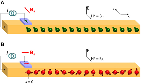
Figure 3. (A) A narrow 2DEG channel extends along the x−axis and has spin polarizing FM injector (purple rectangle). In the nonlocal geometry, a fraction of the injected electrons have ballistic trajectories along . There is no gate voltage, but an intrinsic electric field E results as a spin orbit effect associated with an asymmetry in the confining potential. A strong Rashba spin orbit interaction results in an effective magnetic field for electrons moving with Fermi velocity, vF, x. When an external field Ba sets the injector magnetization to be along ŷ, the injected electrons have spin orientation along ŷ (green spheres). There is no torque from BR and the electrons retain their spin orientation all along the trajectory. (B) When the external field Ba sets the injector magnetization to be along , the injected spin orientation is along and the spin moment of the electron (red spheres) precesses along its trajectory.
A FM electrode detector can be added to the structure with its magnetization also along the x-axis. The detector voltage then will be relatively high (low) when the spin orientation of the ballistic carrers in the vicinity of the detector is parallel (anti-parallel) with (Figure 4A). When ℓ ≪ L, carriers have ballistic trajectories from injector to detector and Datta and Das predicted that the channel conductance of the Spin FET would oscillate periodically as a function of monotonically increasing gate voltage. This effect is an analog of Larmor waves, but the controlling experimental parameter is an electric field rather than a magnetic field. While Larmor waves may be detected along with a diffusive TESR feature in a bulk metal, the Rashba SOI in a spin FET is very large and the spin relaxation rate 1∕τs is very rapid. There is no spin accumulation because injected spin orientation becomes random after only a few scattering events and the Hanle effect, which is the diffusive analog, is not observed. The spin diffusion length, , in InAs 2DEG structures should be very short. However, high values of mobility and large diffusion constants result in λs values that are sufficiently long to be measured.
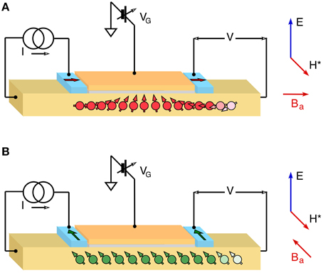
Figure 4. Schematic representation of the Datta-Das experiment, adapted to the NLSV geometry. The distance L between ferromagnetic injector and detector is fixed and is less than a ballistic mean free path. The channel between source and drain can be gated. (A) The injected electrons have spin orientation along ŷ and the orientation is not affected by gate voltage VG. (B) The electrons are injected with spin orientation along and precess under a torque from BR(−ŷ). As VG is varied, the wavelength λ changes and the detector records a conductance oscillation ΔR(VG). Reproduced from Koo et al. [22].
2. Samples and Methodology
Sections 3.2 and 3.3 below review coherent ballistic spin transport experiments and Section 3.1 reviews measurements of spin diffusion. Spin diffusion experiments use the standard nonlocal lateral spin valve geometry and methodology. Studies of ballistic spin effects use the Datta Das Spin-FET design that is modified by adopting the Nonlocal Lateral Spin Valve geometry. Two techniques have been used to observe coherent spin precession: (i) Ballistic spin polarized electrons are injected at x = 0 and the spin orientation is measured as a function of x, . In this case, there is no gate voltage and spin precession is a result of the intrinsic Rashba spin orbit parameter and the effective magnetic field that provides a torque on the spin magnetic moment of the ballistic electrons. (ii) Ballistic spin polarized electrons are injected at x = 0, the spin orientation is detected at x = L, and a gate voltage is applied to the channel to modulate α and RB, y while measuring . In this case, changing the magnitude of RB, y changes the wavelength λ(α) and the detector voltage at fixed L varies between the peak and trough values. The Datta Das technique (ii) was used for the first experimental demonstration [22] of the conductance oscillation. However, method (i) is a novel technique that gives a dramatic demonstration of the Datta Das waves and this will be presented first. This method uses ferromagnetic film electrodes and the intrinsic Spin Hall Effect for injecting and detecting spin polarized carriers. Along with observing two wavelengths of conductance oscillation, this technique also provided the first demonstration of the ballistic intrinsic Spin Hall Effect [23].
2.1. Intrinsic Spin Hall Effect
The description of technique (i) benefits from a brief review of the spin Hall effect (SHE) mechanisms, both direct (DSHE)[24] and inverse (ISHE) [25], with the aid of Figures 5A,B, respectively. In Figure 5A, an unpolarized current J flows along (initial electron velocity is along ), in a material with large SOC. The spin Hall force , proportional to the vector cross-product of the carrier velocity and spin, , has opposite sign for electrons with up- and down-spin. The force derives from a side jump or skew scattering mechanism in extrinsic SHE materials, and is related to band structure in intrinsic SHE materials.
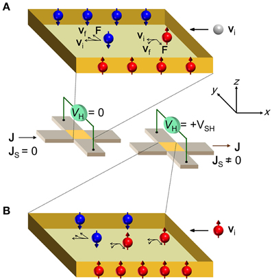
Figure 5. Schematic descriptions of the direct (A) and inverse (B) spin Hall effects. “(A) DSHE. Unpolarized current flows, with initial electron velocity vi along , in a material with strong spin-orbit interaction. Spin Hall force has opposite sign on electrons with opposite spin. Down-spin (up-spin) electrons [blue (red) spheres] are pushed along the positive (negative) y direction, creating equal populations of spin-polarized electrons on opposite sides of the sample. Inset: A Hall voltage measurement shows VH = 0. (B) ISHE. When has more up-spins than down-spins, it's a spin polarized current, . In response to , there are unequal populations on opposite sides. A Hall measurement gives the spin Hall voltage, VH = VSH, proportional to the population difference.” Figure and caption are reproduced from Choi et al. [23].
Down-spin (up-spin) electrons are pushed along the positive (negative) y direction and the result is that spin accumulation develops on both sides of the sample, with opposite spin orientation on opposite sides. An open circuit measurement of Hall voltage would show VH = 0 because the populations are equal, but a single domain ferromagnetic electrode could be used to detect the spin population on either side. In Figure 5B, the electric current is a spin polarized current, JS (JS ≠ 0), dominated by up-spins. The force is the same, but the unequal number of spins results in unequal nonequilibrium populations on opposite sides of the sample. Thus, a Hall measurement would result in a voltage, VH = VSH, that is proportional to the difference in spin populations. The extrinsic SHE in diffusive transport systems has formed a cornerstone of semiconductor spintronics research for the past decade. The intrinsic SHE derives from band structure and can exist in a pure sample, with no scattering. A unique probe of the ISHE is provided by ballistic transport because extrinsic effects do not exist in the absence of scattering.
2.2. Indium Arsenide Single Quantum Wells
The indium arsenide materials system is nearly ideal for empirical realization of the Spin-FET and observation of the predicted Datta Das conductance oscillation. Carriers in the 2DEG of a SQW heterostructure have high mobility (μ), low sheet resistance (R□, resistance per □), and long ballistic mean free path (ℓ) over a large range of temperature, and the Rashba spin orbit interaction (α) is quite high. A typical heterostructure is depicted in cross section in Figure 6A. The center of the SQW is 36.5 nm below the wafer surface. Bilayers of InAlAs/InGaAs form both the top and bottom barrier layers. Doping is provided by an n+ layer of InGaAs below the SQW, and this asymmetry in the heterostructure contributes to the asymmetry in the SQW confining potential [26]. The top indium arsenide layer is a thin chemically stable cap that protects the heterostructure.
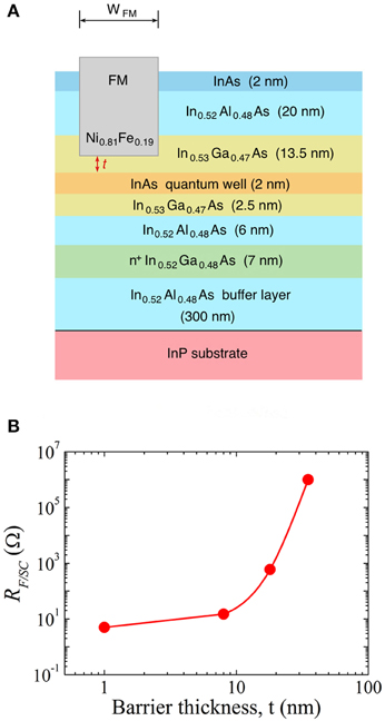
Figure 6. (A) Cross-section of InAs SQW heterostructure and FM electrode. During fabrication of the FM electrode, a trench is made by an ion mill etch, leaving a distance t to the top of the QW. Permalloy is deposited in the trench. (B) Interface resistance, RF∕2DEG, as a function of thickness t. The interface area is about 15 square microns. Reproduced from Chang et al. [27].
Fabrication of a ferromagnetic electrode also is represented in Figure 6A [26]. Observations about the large difference in the resistivities of ferromagnetic metals (FM) and semiconductors resulted in false concerns about the efficiency of spin injection at a FM/2DEG interface. In the original “resistance mismatch” theory [8], the “spin resistances” of the ferromagnetic and nonmagnetic materials must be compared with the resistance of the interface, Ri. The spin resistance ri (i = f or n) is the resistance of a material with unit area and length L′, where , and is given by ri = ρi λs, i. When the interfacial resistance Ri (normalized to unit area) is dominant, Ri > rf, rn, spin injection is efficient. In the regime rf or rn > Ri, self-diffusion of spin accumulation can drive spin polarized carriers from N back into F and diminish the efficiency of spin injection, P → 0. However, empirical results have shown that very large values of Ri will result in negligible values of P and the regime Ri ≫ rf, rn is to be avoided.
A careful and extensive set of NLSV experiments measured the correlation between interface resistance and polarization efficiency [26]. Using the heterostructure of Figure 6A, a channel with width wc = 30μm was formed using optical lithography and dry etching. The pattern for the two ferromagnetic electrodes, each a narrow rectangle of width wFM1 = 400 nm and wFM2 = 500 nm and spanning the width of the channel, was defined by optical lithography. Before deposition of the ferromagnetic metal (Permalloy), portions of the top barrier layer of the heterostructure were etched by ion mill. The depth of milling is characterized by the remaining thickness t of InGaAs that covers the InAs quantum well. For interfaces with areas A of about 15 μm2, the resistance RFM∕SC (the same as the notation Ri used above) was measured and the magnetoresistance experiments using the completed NLSV devices determined the spin injection efficiency, P(RFM∕SC). The dependence of Ri on thickness t is plotted in Figure 6B [27]. Resistance RFM∕SC shows only small variation for the range 1 < t < 10 nm. The product of interface area and resistance was in the range RFM∕SCA = 20 to 50 Ωμm2 and the deduced polarization was consistently P = 1.8 ± 0.2%. For t > 10 nm, the polarization dropped rapidly to zero. The importance of the plateau region, 1 < t < 10 nm, is that samples made with a given value t had highly reproducible values of P.
The barrier layers in typical InAs SQW heterostructures have low transmission but are not as highly resistive as the barriers for other 2DEG materials systems such as GaAs/AlGas. This means that spin injection can be achieved by fabricating a ferromagnetic electrode directly on top of a top barrier layer. Polarization efficiencies are relatively low (~ 2%, but such interfaces also are highly reproducible.
3. Experimental Results
A demonstration of the ballistic Spin-FET and the Datta Das conductance oscillation has been the primary focus of semiconductor spintronics research since 1990. However, the goal of demonstrating electrical spin injection and detection was a necessary prelude, and this goal was elusive for a long time.
3.1. NLSV Magnetoresistance Measurements
An early experiment demonstrated electrical spin injection using a single ferromagnetic metal electrode and an InAs SQW [20, 28]. A rigorous theory was developed [29] and the technique has been used to measure the Rashba spin orbit parameter, α, in single quantum wells [30]. The results were corroborated by Shubnikov de Haas measurements and the method is more convenient because it does not require a large magnetic field.
An indium arsenide SQW with Permalloy electrodes was used for the first demonstration of both electrical spin injection and detection in a nonlocal lateral spin valve [21]. The sample heterostructure was grown by molecular beam epitaxy. The two dimensional electron gas is confined to a 15 nm thick InAs layer by barrier layers. The top barrier is a 25 nm layer of Al0.6Ga0.4Sb and the bottom barrier is a 200 nm layer of Al0.6Ga0.4Sb. The carriers are provided by electron doping resulting from a 60 s As soak during deposition of the top AlGaSb layer. The asymmetry of the confining potential results from the doping in the top layer. An estimate of the Fermi level, measured from the bottom of the InAs conduction band, is 200 meV. The mobility, carrier density and sheet resistance at 296 K (77 K) were found, using Hall measurements (before processing), to be 25, 000 cm2 V− 1 s− 1 (70,000 cm2 V− 1 s− 1, 1.3 × 1012 cm− 2 (8.7 × 1011 cm− 2), and 190 Ω∕□ (80 Ω∕□), respectively [20]. Magnetoresistance measurements were performed by applying an in-plane magnetic field along the easy magnetization axes of the ferromagnetic injecting and detecting electrodes. Hysteretic dips of magnitude ΔR were observed in the field ranges where the FM magnetizations are reversing. Measurements were made for two values of channel length between injector and detector, L = 3.2 and 10.6 μm, in the temperature range 4 K < T < 150 K. The ballistic mean free path was measured to be ℓ = 1.2 μm below T = 50 K. With measurements of ΔR for only two values of L and a long carrier mean free path, a model for the data could neither discriminate between ballistic and diffusive transport nor determine the spin diffusion length. The magnitude of ΔR was about 0.3Ω (0.05Ω) at L = 3.2 μm (10.6 μm).
A few years later, a careful set of experiments measured the spin diffusion length λs, and spin relaxation time τs, in an InAs 2DEG over a temperature range 20 < T < 295 K [31]. Of equal importance, these experiments provide a measurement of polarization, P. A set of samples was fabricated using the SQW heterostructure and FM/2DEG interface shown in Figure 6A. The barrier thickness between the top of the InAs QW and the bottom of the Permalloy electrode was measured by TEM to be t = 7 ± 2 nm. The carrier density and mobility of the 2DEG were n = 6.3 × 10¹² (4.6 × 10¹²) cm− 2 and μ = 5, 700 (34, 700) cm2 V−1 s−1 at 295 K (20 K) [31]. The channel width was wc = 8 μm, the injector and detector electrode widths were wF1 = 500 nm, wF2 = 2.0 μm, and devices with center to center spacings of L = 2.2, 2.5, 3.8, 4.6, and 6.2 μm were measured at temperatures T = 20, 50, 100, and 295 K. Hysteretic dips of magnitude ΔR were observed in the field ranges 100–250 Oe when external field was swept up, and −100 to −300 Oe, when external field was swept down. At each temperature, data were analyzed as a function of injector/detector separation, ΔR(L). The magnitude of the dips was ΔR ≈ 2.2 mΩ at L = 2.2 μm and it decreased exponentially with increasing L. Fits to the expression [32]
where R□ is the 2DES sheet resistance, permitted a determination of the fractional polarization P of injector and detector. The following values were found: λs = 1.8, 1.9, 1.5, and 1.3 μm and P = 1.9, 1.7, 1.7, and 1.4% at temperatures 20, 50, 100, and 295 K. The relatively large width of the ferromagnet detector, wF2 = 2.0μm >λs, limits the accuracy of the results. However, the study had several important observations: (i) the polarization efficiency P is highly reproducible from sample to sample and through a wide range of temperature, for samples fabricated to have carefully controlled interfaces; (ii) the spin diffusion length is approximately 2μm and is weakly dependent on temperature; and (iii) the spin relaxation time, τsf, is roughly 5 psec at cryogenic temperature and is weakly dependent on temperature, rising by a factor of about 2 at room temperature. These characteristics are expected to be valid for any InAs heterostructure with a narrow SQW (2 nm, in these samples).
3.2. Conductance Oscillation Observed with Variable L
Successful experimental observation of the Datta Das conductance oscillation was achieved by using an indium arsenide SQW with high mobility and high spin orbit coupling [22]. A recent set of experiments demonstrated a novel technique for observing coherent spin precession in a 2DES channel. This technique uses a ferromagnetic film electrode for spin injection and the intrinsic ISHE for detecting , and two full wavelengths of conductance oscillation have been observed [23].
The technique follows the concept of Figure 3 and details are explained with the aid of Figure 7. An electron with initial spin angular momentum Sx is injected at x = 0. The spin orientation precesses under the torque of effective field BR(−ŷ) and the spin orientation along the ballistic trajectory has wavelength λ. By the end of the trajectory, at x ≈ ℓ, the spin has accumulated a relative phase angle Δθ that is several multiples of 2π if λ < ℓ. The spin Hall effect force is a cross product of and and is perpendicular to both. Along the trajectory, is maximum when is along the z − axis, Δθ(x) = mπ∕2 (m odd), and VH has maximum value, either positive or negative. When is along the x−axis, Δθ(x) = mπ∕2 (m even), is zero and VH = 0. In a heuristic picture (Figure 7B, red trace), the trajectories are deflected along ±ŷ in a sinusoidal way. The nodes are at positions with oriented along and the antinodes have oriented along ±ẑ. A Hall cross at an arbitrary value of x (Figure 7A) records an inverse spin Hall voltage proportional to the deflection. A series of Hall crosses at positions xi will record voltages VH, i(x) and a plot of VH, i(x) will show a conductance oscillation (Figure 7C, blue line) with wavelength predicted by Datta and Das [10]
where ℏ is Planck's constant divided by 2π and α is the Rashba spin-orbit parameter. For the experiments of Choi et al. [23], it was not feasible to fabricate a single channel with multiple Hall detectors in the configuration of Figure 7A. Instead, the authors fabricated several identical nonlocal intrinsic Hall effect devices and the discrete channel length L was systematically varied. The model described above gives a prediction for VH(Δθ(L)) for each L. A fully rigorous model would develop a Hamiltonian in which the spin Hall force results in a lateral periodic potential.
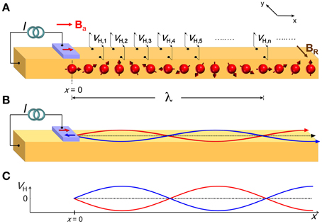
Figure 7. (A) Applied field Ba controls the magnetization orientation of the ferromagnetic injector along (red arrow on FM). Red spheres represent spin polarized electrons injected at x = 0. As described in Figure 3B, these carriers move in the nonlocal region with spin precession. A series of Hall detectors, VH, i, is arrayed along the channel in the region x > 0. (B) “Deflection of ballistic trajectories caused by the intrinsic spin Hall effect. dotted line: trajectory with no deflection. red: trajectory for magnetization along +x. blue: trajectory for magnetization along −x (blue arrow on FM). (C) Hall voltage in region x > 0 as a result of inverse spin Hall effect.” In (A), a set of Hall cross detector at discrete distances x = Li determine the phase of the spin of the ballistic electron because is proportional to the local spin Hall voltage, VSH. Figure and portion of caption reproduced from Choi et al. [23].
The devices were fabricated using the high mobility InAs SQW of Figure 6A. The following sample characteristics were determined (at 1.8 K): carrier density n = 2.0 × 1012 cm2, mobility μ = 60, 000 cm2V−1s−1, and mean free path ℓ = 1.61 μm. From the beat frequency in Shubnikov de Haas measurements [22], the Rashba spin-orbit parameter was found: α = 8.93 × 10⁻¹² eV-m, at VG = 0. Using these numbers and ( kg), the Datta-Das wavelength can calculated, λ = 0.54 μm (< < ℓ = 1.6 μm).
Figure 8 is a sketch of the geometry of each device. Each Hall cross with FM electrode is formed using electron beam lithography. The centre-to-centre distance L between FM and the Hall arm is measured from a scanning electron micrograph. A set of experiments reports results [23] from 15 ungated devices, 14 having wC = 0.75μm as channel width and variable length L. A single device had width wC = 6.0μm. The sixteenth sample was fabricated with the Hall cross and FM electrode covered by a 110 nm thick dielectric and a 5 nm/80 nm thick Ti/Au gate.
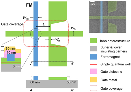
Figure 8. “Schematic top and cross-section views of geometry of each individual device. The single quantum well channel and Hall cross are formed by subtractive processing using electron beam lithography and an Ar ion mill. The FM electrode is deposited after a portion of the top barrier of the InAs heterostructure is etched. wH = 200 nm, wFM = 400 nm. Distance L is measured center-to-center. A single sample is fabricated with dielectric and gate layers that cover the entire device region.” This sample is discussed in Section 3.4. Inset: Scanning electron micrograph of a device with wC = 750 nm, L = 1.32 μm. Figure and portion of caption reproduced from Choi et al. [23].
Measurement of the ISHE used the approach introduced for detecting the spin Hall effect in aluminum films [25]. For any device, changing injected spin orientation between +Sx and −Sx alters the local spin component Sz between +Sz and −Sz and ΔVH is measured as the difference of VH. The initial orientation of the injected spins is controlled by manipulating the FM magnetization, which is changed between +Mx and −Mx by using an external field Ba, x. Since there is never a field with component perpendicular to the Hall cross plane, Ba, z = 0, there is no classic Hall effect. An example of the experimental methodology of Choi et al. is shown in Figure 9 using data from a device with wC = 6μm. These data will be used for a comparison with Spin FET results described below. The length of the channel, L = 2.83μm, corresponds to 5.25λ (m = 21) and the accumulated phase Δθ determines the local spin orientation of ballistic electrons, , to be along +ẑ. The deviation of ballistic trajectories is maximum (antinodes in Figure 7) and ΔVH has maximal value.
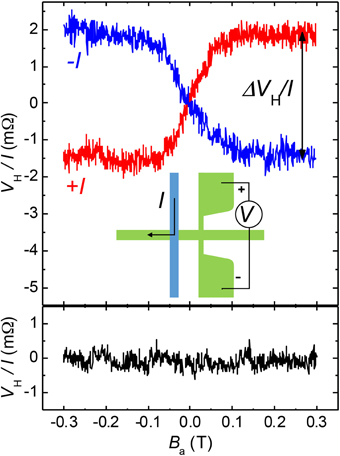
Figure 9. Data showing the intrinsic inverse spin Hall effect. Sample: wC = 6.0 μm, L = 2.83 μm, I = 1 mA, T = 1.8 K. Magnetic field Ba is applied along the . Red trace: I positive. Blue trace: I negative. ΔVH ≡ VH(Ba > 0.2 T)−VH(Ba < 0.2 T). The measurement geometry is shown in the inset Bottom panel: Control experiment described in the text. Spins are injected with orientation along the y−axis, parallel with BR. There is no spin precession and the spin Hall voltage is zero. Reproduced from Choi et al. [23].
Referring to Figure 9, we begin by describing the data for the case of zero field (Ba = 0). Here the magnetization aligns along the y−axis, because of the FM shape anisotropy. Injected electrons have initial orientation along ±ŷ, there is no spin precession because F = 0 (refer to Figure 3A), and VH(Ba = 0) = 0. Increasing the magnitude Ba tips MFM toward and the injected spins acquire a component along the x−axis. The spins now precess, and a nonzero spin Hall voltage is measured because has a component along z at x = L. For magnitudes of Ba = 0.12 T or larger, is saturated along the x−axis, for Ba > 0.12 T (Ba < 0.12 T), because the applied field overcomes the shape anisotropy. Anisotropic magnetoresistance (AMR) measurements are used to characterize the magnetization state of the FM electrode [22, 23]. Narrow, thin film FM wires are expected to have structural imperfections that might result in randomly pinned domains, especially at the edges. However, the AMR data show fields with magnitude greater than 0.12 T are sufficiently large to fully saturate the magnetization. Thus, injected spins have initial orientation directly along the x−axis, is along z at x = L, and therefore both F and VH are at maxima. Reversing the bias current polarity (Figure 9, blue lines) results in an opposite orientation of the injected spins and the sign of the intrinsic spin Hall voltage is reversed. The magnitude of the intrinsic inverse spin Hall effect is measured to be ΔRH = ΔVH ∕ I = 3.6 mΩ. In a control experiment (bottom panel of Figure 9), field Ba is applied along the y−axis and is always along ±ŷ. Injected spins have initial orientation along the y−axis, there is zero torque and no spin precession (refer to Figure 3A). It follows that F = 0 for all x, and VH = 0 for the entire range of Ba. Converse measurements demonstrate the ballistic intrinsic DSHE on the same sample. The vertical arms of the Hall cross are biased with a current and the spin Hall effect creates spin-up (spin-down) electrons with velocity components along the −x (+x) direction near the left (right) side of the Hall cross region. The ballistic trajectories of a fraction of these carriers extend to the vicinity of the FM film, which now performs as a spin detector. Measurements using this converse geometry give the same result as the inverse spin Hall experiment, ΔRH = ΔVH ∕ I = 3.6mΩ.
With this understanding of the measurements of each device, we next describe the experiments introduced conceptually in Figure 7A. As noted above, a set of 14 individual samples was used [23]. Each device was fabricated to have width wC = 0.75μm and the channel length L varied from the values 0.64 to 1.72 μm. Figure 10A shows examples of data and it's important to note that the sign of ΔRH can be either negative or positive. Figure 10B plots values of ΔRH(L) and two complete wavelengths of the conductance oscillation predicted by Datta and Das are observed. The fit represented by the dotted line in the figure uses the wavelength λ of Equation (2),
where A is the measured amplitude. The solid line modifies the above expression by including an exponential decay e−L∕ℓ, where the ballistic mean free path was independently determined [22] (ℓ = 1.61 μm). The only free fitting parameter is the amplitude, experimentally measured as ΔRH for the sample device with L = 0.64 μm. It's important to note that there is no arbitrary phase shift in the data of Figure 10; the data values are determined only by the injector and detector distance L. The data in Figure 10B represent a graphical demonstration that the results of all devices fit the Datta-Das model presented above [23]. Furthermore, these data confirm the absence of scattering because the conductance oscillation requires ballistic transport. It follows that the detected inverse spin Hall effect must be intrinsic.
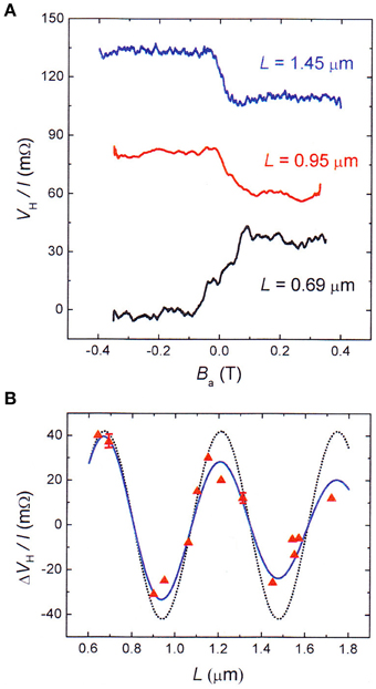
Figure 10. Dependence of the inverse spin Hall voltage on channel length. (A) “Examples of inverse spin Hall voltages for several lengths L. Data are offset for clarity. Baseline (offset) resistances RB are 170 mΩ, 360 mΩ, and 2.4 Ω for L = 0.69, 0.95, and 1.45 μm, respectively. The value RB = 2.4Ω is much larger than ΔRH(L = 1.45μm) = 23 mΩ, but less than 3% of the channel resistance. (B) ΔRH as a function of channel length L. wC = 0.75μm, I = 0.1 mA, T = 1.8 K. Dotted line fit is from the ballistic transport model, Equation (3). Solid line fit is the same model modified to include the exponential decay of ballistic trajectories. Error bars are smaller than symbols except where shown.” Figure and portion of caption reproduced from Choi et al. [23].
3.3. Conductance Oscillation Observed with Variable VG
In the original Datta-Das proposal, the conductance of a Spin FET with fixed separation L between source and drain was predicted to oscillate periodically as the gate voltage was varied monotonically. The experiment required a measurement of ΔR(VG) and was first successfully realized by Koo et al. [22]. The devices, sketched in Figure 4, were comprised of an InAs high electron mobility SQW channel (Figure 6A) covered by a dielectric and a metal gate electrode. Ferromagnetic (Ni81Fe19) electrodes were fabricated on top as spin polarizing source (injector) and spin sensitive drain (detector). The carrier mobility and density of the 2DEG were μ = 50, 000−60, 000 cm2 V−1s−1 and cm−2, respectively, at T = 1.8 K. A dry mesa etch defined the channel, having a width wc = 8μm. Electron beam lithography and lift-off were used to fabricate the two ferromagnetic electrodes with lateral dimensions of 0.4 μm by 80 μm and 0.5 μm by 40 μm. Samples with two values L of channel length, L = 1.25 and 1.65 μm measured center to center, were fabricated and measured.
Figure 11A shows examples of the Datta-Das conductance oscillation. A magnetic field, with magnitude Ba, x = 0.5 T, is externally applied to orient the source and drain magnetizations in the chosen direction (parallel with ), thereby setting the spin injection/detection axis. The gate voltage is varied monotonically over the range −3 ≤ VG ≤ 3 V while the nonlocal channel conductance is measured. Describing the red trace (L = 1.65μm) first, the injected spin orientation also along +x and is perpendicular to the Rashba field. An oscillation of the voltage detected at the drain, as a function of gate voltage VG, is observed because the rate of spin precession is proportional with gate voltage. The range of VG is sufficiently large that Figure 11A shows more than a full cycle of conductance oscillation. Data for a similar Spin FET, with L = 1.25μm, also are shown in Figure 11A (black trace). As discussed below, the oscillation has a longer wavelength in a Spin FET with shorter channel length.
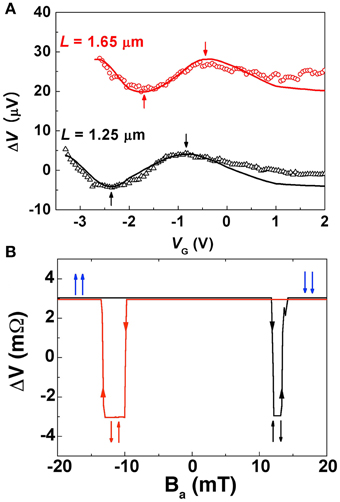
Figure 11. (A) Datta Das conductance oscillation for two values of L. Symbols: data. Solid lines: fits. Details of the fits are found in Koo et al. [22] and Zainuddin et al. [33]. (B) NLSV magnetoresistance measurements using a small, variable in-plane field, Ba, y. I = 1 mA. The magnitude ΔR of the dips is used as the amplitude A in the fits in (A). Reproduced from Koo et al. [22].
A set of several experiments gave further confirmation that spin precession in the channel was the only source of the voltage oscillation. Using the technique described in the previous section, a field Ba externally applied along ŷ orients the source and drain magnetization to lie along ŷ. In this case the injected spin orientation is parallel with the Rashba field. There is no torque on the ballistic spins, they do not precess [Figure 4B], and the voltage recorded by the detector shows no modulation. Further tests were made using specially fabricated control devices and identical transport measurements. The same geometry and lithographic processing steps were used, but a nonmagnetic electrode film [indium (50 nm)/Au (30 nm)] was used for the detector. No voltage modulation was observed for any field configuration.
The conductance oscillations shown in Figure 11A were quantitatively analyzed with only a single free fitting parameter, a small arbitrary phase shift, and the procedure is discussed in detail below [22]. The analysis required direct measurements of the oscillation amplitude A and the Rashba SOC, α(VG), for the range of gate voltages applied. The amplitude was determined using standard nonlocal lateral spin valve magnetoresistance measurements and an in-plane magnetic field externally applied along the y−axis (Figure 11B). As described earlier in Section 3.2, the bias current is held constant and the voltage Vd at the detector is recorded as a function of field Ba, y. The voltage is positive when the injector and detector magnetizations, M1 and M2, are parallel (refer to arrows in Figure 11B). Magnetizations M1 and M2 are antiparallel in the small range of field between the two values of switching field, and the voltage is negative. The hysteretic dips that were observed had magnitude A = ΔV = 6 ± 0.2 μV (ΔR = 6 ± 0.2 mA). This measurement, at T = 1.8 K and L = 1.65μm ≈ ℓ = 1.61μm, is in a ballistic transport regime where no theory is available to analyze the magnitude of the resistance dips. However, the measurements shown in Figure 11A use the same device and are in the same transport regime. The resistance difference between wave peak and trough represents the difference between detection of spins parallel and antiparallel with the detector magnetization, which is the same difference measured in Figure 11B. The measured value of A is therefore used as the amplitude of the fit in Figure 11A. To determine the Rashba parameter α(VG), Shubnikov-de Haas oscillations were measured and the observed beat patterns were analyzed [22]. As examples of several parameters of interest, the Rashba spin orbit parameter with zero gate voltage is α(0 V) = 9.0 × 10⁻¹² ev-m and the magnitude of the effective magnetic field (also at zero gate voltage) is BR, y = 8.5 T.
The fits shown in Figure 11A were generated using the theory of Datta and Das [10] for the voltage recorded at the detector
The values of A and α(VG) were independently measured, as described above. In the above equation, ϕ is a small phase shift that may be related to shielding effects from the ferromagnetic films. The quality of both fits (red and black solid lines in Figure 11A) is excellent. The two data sets, for L = 1.65 and L = 1.25 μm, can be discussed by comparing their half-wavelengths. As the channel length L decreases from 1.65 μm to 1.25 μ the half-wavelength increases from ΔVG = 1.24 to 1.53 V. Thus, it is seen that the Datta-Das theory successfully describes the dependence of the oscillation with channel length. The detailed shape of the fit has been reproduced by numerical simulations [33] that are accompanied by a physical explanation.
3.4. Gate Voltage Controlled Conductance Oscillation with ISHE Detection
Gate voltage controlled spin precession in a spin-FET with an ISHE detector has been demonstrated [23]. A gated device was prepared (wC = 0.75μm, L = 0.9μm; refer to Figure 8) and the experimental technique was very similar to that described in the previous section. The magnetization of the ferromagnetic injector (“FM” in Figure 8) is in the film plane. An external field is applied along , the shape anisotropy along the y−axis is overcome, and spin polarized electrons are injected with spin orientation along . The voltage at the spin Hall detector is recorded for variable gate voltage, −4V < VG < +3.2V. Data in Figure 12 show the voltage detected by the ballistic intrinsic ISHE and a bias current of I = 0.1 mA. The voltage oscillates according to the Datta Das prediction, Equation (4), with A the measured amplitude. The solid line fit is calculated from Equation (4) using the measured values α(VG) (1.46 × 10⁻¹¹ eV-m to 8.01 × 10⁻¹² eV-m for the experimental range of VG) [22].
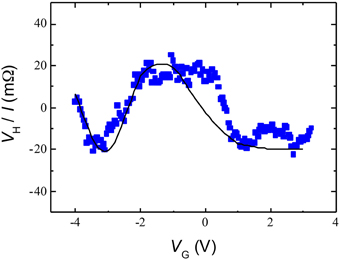
Figure 12. Datta Das conductance oscillation for FM injection and ISHE detection. Symbols: data. Solid line: fit. Details of the fit are found in Koo et al. [22] and Zainuddin et al. [33]. wC = 750 nm; L = 900 nm; T = 1.8 K; I = 0.1 mA. Baseline resistance is RB = 4mΩ. Reproduced from Choi et al. [23].
4. Discussion
4.1. Two Dimensional Channel vs. Narrow Channel
The oscillation shown in Figure 10 shows good signal-to-noise and it's remarkable that two full wavelengths are observed. Two mechanisms that might degrade the oscillation can be mentioned. First, the epitaxially grown SQW heterostructure may contain small structural imperfections. Even at the scale of one nanometer, such imperfections could result in small variations in the confining potential and associated spatial variations in the spin-orbit parameter, α. Spin phase coherence relies on a constant value of α, and variations would weaken the phase coherence of the ballistic electrons and diminish the amplitude of the conductance oscillation. Second, the side edges of the SQW channel, fabricated by electron beam lithography and a mesa etch, likely are characterized by spatial roughness. The lack of smooth and linear edges promotes diffusive scattering and may diminish the number of ballistic carriers and this may diminish the magnitude of the detected oscillation.
Next, we compare the data in Figures 11A, 12. It's obvious that the oscillation has larger magnitude in the data of Figure 12. The larger amplitude could be related to several different factors: (i) higher detection efficiency in samples with ISHE detection, (ii) narrower channel width, 750 nm compared with 8 μm; or (iii) shorter channel length L. For consistency of all comparisons, we use either the peak to peak magnitude of the gate voltage controlled oscillation or, for zero gate voltage, we choose a position L that corresponds to a peak amplitude ( along ẑ).
Noting that both kinds of samples used the same Permalloy injector, the relative detection efficiency of F electrodes and ISHE Hall crosses can be tested by comparing the oscillation amplitude for samples with comparable channel widths, at comparable channel lengths. An ISHE device had channel width wc = 6μm, length L = 2.83μm and the value ΔRH = 3.6±0.2 mΩ. The spin FET with F detector had channel width wc = 8μm, length L = 1.65μm and the peak to peak magnitude was ΔRSV = 6.0±0.2 mΩ. We extrapolate the results of the latter to the length of the former in order to compare, using a simple exponential factor governed by the decay of the ballistic mean free path [23], exp[−(2.83−1.65)∕1.6]. The comparison, ΔRSV = 2.9±0.2mΩ and ΔRH = 3.6±0.2 mΩ, shows values that are nearly the same and we deduce that the efficiency of detection using ballistic ISHE is about the same as detection using a Permalloy ferromagnetic electrode.
The width of the channel can be expected to influence the oscillation magnitude. The original Datta Das derivation was based on a one-dimensional channel. A device with a single Landauer conductance mode would show the maximum possible amplitude. However, Datta and Das also noted the absence of momentum in the final solution for the spin phase accumulated by a carrier that moves ballistically from source to drain. This implies that contributions to the oscillation are not restricted to carriers with momentum . Instead, carriers with some component of transverse momentum, , will contribute to the oscillation with the same phase. In fact, Datta and Das noted that carriers from a higher energy sub-band also could contribute with the same spin phase. Because of the lack of any restriction on , the first successful experiment was able to observe the oscillation in a channel so wide that it was two-dimensional.
Nevertheless, a relatively small number of ballistic trajectories, those with only small components ky, reach the detector with no scattering in a wide channel sample. Trajectories with a large component ky will scatter and lose spin phase coherence. In a narrow channel, carriers with , or with very small components ky, are injected into the device and have a high probability of reaching the detector with no scattering. During the injection process, carriers with large components ky will have no available states in the 2DEG and will be reflected at the interface. This model presents a purely geometric effect, which is expected in samples with many Landauer modes.
To test the effect of channel width, we compare the oscillation amplitude of two samples with ISHE detection, having channel widths 6 μm (L = 2.83μm) and 750 nm (L = 1.74μm). Both lengths represent antinodes (oscillation peak), and we extrapolate the latter to the length of the former by using the same exponential decay factor. The comparison, ΔRH (wc = 6μm) = 3.6mΩ and ΔRH (wc = 0.75μm) = 10 mΩ, shows that shrinking the channel width by a factor of about eight leads to an amplitude increase by a factor of about three.
Diminishing the channel length L from L = 1.65μm (Figure 11A) to L = 0.90μm (Figure 12) accounts for another factor of two because of the exponential dependence on mean free path. Further increases in the magnitude of the oscillation can be achieved by shrinking the width and shortening the length of the channel. Using sophisticated electron beam lithography techniques, it's quite possible to expect a further increase of a factor of ten or more. Observation of the oscillation at elevated temperatures requires using a SQW with long mean free path at room temperature.
5. Conclusion
This article has reviewed phenomena of spin dependent transport that are uniquely suited for observation in the indium arsenide materials system. These phenomena are extensions of the spin injection phenomenology. Techniques of conduction electron spin injection and detection were reviewed, and characteristics of ballistic and diffusive spin transport were discussed. Early demonstrations of spin injection, diffusive transport, and spin detection in InAs quantum wells were presented. Rashba Spin Orbit Coupling (SOC) in a single quantum well heterostructure was introduced. The remarkable prediction, by Datta and Das, that spin polarized ballistic electrons in the channel of a spin injected field effect transistor (Spin FET) would show coherent spin precession resulting from the torque of a Rashba effective magnetic was described. This coherent spin precession was predicted to be observable as a source-drain conductance oscillation. Successful empirical observation of the conductance oscillation was enabled by employing the nonlocal lateral spin valve geometry. Two different techniques for observing this oscillation were reviewed. A brief discussion compared these techniques and discussed scaling and dimensionality effects of the phenomena.
Conflict of Interest Statement
The authors declare that the research was conducted in the absence of any commercial or financial relationships that could be construed as a potential conflict of interest.
Acknowledgments
MJ gratefully acknowledges the support of the Office of Naval Research and the Naval Research Laboratory Nanoscience Institute. HK, SH, and JC gratefully acknowledge the support of the Korean Institute of Science and Technology.
References
1. Mott NF. The electrical conductivity of transition metals. Proc R Soc A (1936) 153:699. doi: 10.1098/rspa.1936.0031
2. Tedrow PM, Meservey R. Spin-dependent tunneling into ferromagnetic nickel. Phys Rev Lett. (1971) 26:192. doi: 10.1103/PhysRevLett.26.192
3. Julliere M. Tunneling between ferromagnetic films. Phys Lett A (1975) 54A:225. doi: 10.1016/0375-9601(75)90174-7
4. Binasch G, Grünberg P, Saurenbach F, Zinn W. Enhanced magnetoresistance in layered magnetic structures with antiferromagnetic interlayer exchange. Phys Rev B (1989) 39:4828. doi: 10.1103/PhysRevB.39.4828
5. Baibich MN, Broto JM, Fert AF, Nguyen Van Dau F, Petroff F, Eitenne P, et al. Giant magnetoresistance of (001)Fe/(001)Cr magnetic superlattices. Phys Rev Lett. (1988) 61:2472. doi: 10.1103/PhysRevLett.61.2472
6. Johnson M, Silsbee RH. Interfacial charge-spin coupling; injection and detection of spin magnetization in metals. Phys Rev Lett. (1985) 55:1790. doi: 10.1103/PhysRevLett.55.1790
7. Johnson M, Silsbee RH. The spin injection experiment. Phys Rev B (1988) 37:5326. doi: 10.1103/PhysRevB.37.5326
8. Johnson M, Silsbee RH. Coupling of electronic charge and spin at a ferromagnetic - paramagnetic interface. Phys Rev B (1988) 37:5312. doi: 10.1103/PhysRevB.37.5312
9. Johnson M, Silsbee RH. A thermodynamic analysis of interfacial transport and of the thermomagnetoelectric system. Phys Rev B (1987) 35:4959. doi: 10.1103/PhysRevB.35.4959
10. Datta S, Das B. Electronic analog of the electroopitic modulator. Appl Phys Lett. (1990) 56:665. doi: 10.1063/1.102730
11. Bychkov YA, Rashba EI. Properties of a 2D electron-gas with lifted spectral degeneracy. JETP Lett. (1984) 39:78.
12. Rashba EI, Efros AL. Orbital mechanisms of electron spin manipulation by an electric field. Phys Rev Lertt. (2003) 91:126405. doi: 10.1103/PhysRevLett.91.126405
13. Johnson M. Spin injection, accumulation, and relaxation in metals. In: Tsymbal EY, Zutic I, editors. Handbook of Spin Transport and Magnetism. Boca Raton, FL: CRX Press (1994), pp. 115–136.
14. Janossy A, Monod P. Spin waves for single electrons in paramagnetic metals. Phys Rev Lett. (1976) 37:612. doi: 10.1103/PhysRevLett.37.612
15. Hanle W. Uber magnetische beeinflussung der polarisation der resonanzfluoreszenz. Z Physik (1924) 30:93. doi: 10.1007/BF01331827
16. Valenzuela S, Tinkham M. Spin-polarized tunneling in room-temperature mesoscopic spin valves. Appl Phys Lett. (2004) 85:5914. doi: 10.1063/1.1830685
17. Garzon S, Zutic I, Webb RA. Temperature dependent asymmetry of the nonlocal spin-injection resistance: evidence for spin non-conserving interface scattering. Phys Rev Lett. (2005) 94:176601. doi: 10.1103/PhysRevLett.94.176601
18. Sasaki T, Oikawa T, Suzuki T, Shiraishi M, Suzuki Y, Noguchi K. Temperature dependence of spin diffusion length in silicon by hanle-type spin precession. Appl Phys Lett. (2010) 96:122101. doi: 10.1063/1.3367748
19. Kurn H, Heo J, Johangir S, Banerjee A, Guo W, Bhattacharya P. Room temperature single GaN nanowire spin valves with FeCo/MgO tunnel contacts. Appl Phys Lett. (2012) 100:182407. doi: 10.1063/1.4711850
20. Hammar PR, Bennett BR, Yang MJ, Johnson M. Observation of spin injection at a ferromagnet - semiconductor interface. Phys Rev Lett. (1999) 83:203. doi: 10.1103/PhysRevLett.83.203
21. Hammar PR, Johnson M. Detection of spin-polarized electrons injected into a two-dimensional electron gas. Phys Rev Lett. (2002) 88:066806. doi: 10.1103/PhysRevLett.88.066806
22. Koo HC, Kwon JH, Eom J, Chang J, Han SH, Johnson M. Gate voltage control of spin precession in a spin injected field effect transistor. Science (2009) 325:1515–8. doi: 10.1126/science.1173667
23. Choi WY, Kim HJ, Chang J, Han SH, Koo HC, Johnson M. Electrical detection of coherent spin precession using the ballistic intrinsic spin hall effect. Nat Nanotechnol. (2015) 10:666–70. doi: 10.1038/nnano.2015.107
24. Dyakonov MI, Perel VI. Possibility of orienting electron spins with current. JETP Lett. (1971) 13:467–70.
25. Valenzuela SO, Tinkham M. Direct electronic measurement of the spin hall effect. Nature (2006) 442:176–9. doi: 10.1038/nature04937
26. Park YH, Koo HC, Chang J, Han S-H, Johnson M. High mobility in a two dimensional electron system with a thinned barrier. Sol State Comm. (2011) 151:1599–601. doi: 10.1016/j.ssc.2011.07.022
27. Chang J, Koo HC, Eom J, Han SH, Johnson M. Injection, detection and gate voltage control of spins in the spin field effect transistor. J Appl Phys. (2011) 109:102405. doi: 10.1063/1.3576140
28. Johnson M. Theory of spin-dependent transport in ferromagnet-semiconductor heterostructures. Phys Rev B (1998) 58:9635. doi: 10.1103/PhysRevB.58.9635
29. Silsbee RH. Spin-orbit induced coupling of charge current and spin polarization. J Phys. (2004) 16:R179–207. doi: 10.1088/0953-8984/16/7/R02
30. Park YH, Jang HC, Koo HC, Kim H-J, Chang J, Han SH, et al. Observation of gate-controlled spin–orbit interaction using a ferromagnetic detector. J Appl Phys. (2012) 111:073C317. doi: 10.1063/1.3677936
31. Koo HC, Yi H, Ko J-B, Chang J, Han S-H, Jung D, et al. Electrical spin injection and detection in an InAs quantum well. Appl Phys Lett. (2007) 90:022101. doi: 10.1063/1.2430688
32. Johnson M. Spin polarization of gold films via transport. J Appl Phys. (1994) 75:6714. doi: 10.1063/1.356848
Keywords: spintronics, spin injection, spin polarized current, Datta Das conductance oscillation, Rashba spin-orbit coupling, spin injected field effect transistor (Spin FET), spin transistor
Citation: Johnson M, Koo HC, Han SH and Chang J (2015) Spin injection in indium arsenide. Front. Phys. 3:62. doi: 10.3389/fphy.2015.00062
Received: 11 June 2015; Accepted: 30 July 2015;
Published: 18 August 2015.
Edited by:
Atsufumi Hirohata, University of York, UKReviewed by:
Dong-Hyun Kim, Chungbuk National University, South KoreaYoshiaki Saito, Toshiba Corporation, Japan
At least a portion of this work is authored by Dr. Mark Johnson on behalf of the U.S. Government and, as regards Dr. Johnson and the U.S. Government, is not subject to copyright protection in the United States. Foreign and other copyrights may apply. This is an open-access article distributed under the terms of the Creative Commons Attribution License (CC BY). The use, distribution or reproduction in other forums is permitted, provided the original author(s) or licensor are credited and that the original publication in this journal is cited, in accordance with accepted academic practice. No use, distribution or reproduction is permitted which does not comply with these terms.
*Correspondence: Mark Johnson, US Naval Research Laboratory, 4555 Overlook Ave. SW, Washington, DC 20375, USA, mark.b.johnson@nrl.navy.mil