High-throughput multiple dies-to-wafer bonding technology and III/V-on-Si hybrid lasers for heterogeneous integration of optoelectronic integrated circuits
 Xianshu Luo1
 Yulian Cao2
 Junfeng Song1
 Xiaonan Hu2
Yuanbing Cheng2
Chengming Li2
Chongyang Liu2
Tsung-Yang Liow1
Mingbin Yu1
Hong Wang2
Qi Jie Wang2
Xiaonan Hu2
Yuanbing Cheng2
Chengming Li2
Chongyang Liu2
Tsung-Yang Liow1
Mingbin Yu1
Hong Wang2
Qi Jie Wang2  Patrick Guo-Qiang Lo1*
- 1Institute of Microelectronics, Agency for Science, Technology and Research (A*STAR), Singapore, Singapore
- 2Photonics Center of Excellence (OPTIMUS), School of Electrical and Electronic Engineering, Nanyang Technological University, Singapore, Singapore
Integrated optical light source on silicon is one of the key building blocks for optical interconnect technology. Great research efforts have been devoting worldwide to explore various approaches to integrate optical light source onto the silicon substrate. The achievements so far include the successful demonstration of III/V-on-Si hybrid lasers through III/V gain material to silicon wafer bonding technology. However, for potential large-scale integration, leveraging on mature silicon complementary metal oxide semiconductor (CMOS) fabrication technology and infrastructure, more effective bonding scheme with high bonding yield is in great demand considering manufacturing needs. In this paper, we propose and demonstrate a high-throughput multiple dies-to-wafer (D2W) bonding technology, which is then applied for the demonstration of hybrid silicon lasers. By temporarily bonding III/V dies to a handle silicon wafer for simultaneous batch processing, it is expected to bond unlimited III/V dies to silicon device wafer with high yield. As proof-of-concept, more than 100 III/V dies bonding to 200 mm silicon wafer is demonstrated. The high performance of the bonding interface is examined with various characterization techniques. Repeatable demonstrations of 16-III/V die bonding to pre-patterned 200 mm silicon wafers have been performed for various hybrid silicon lasers, in which device library including Fabry–Perot (FP) laser, lateral-coupled distributed-feedback laser with side wall grating, and mode-locked laser (MLL). From these results, the presented multiple D2W bonding technology can be a key enabler toward the large-scale heterogeneous integration of optoelectronic integrated circuits.
Introduction
In the future generation of datacom and computercom, which demand ever higher bandwidth and lower power, the conventional electrical interconnection routing the electronic signals becomes bandwidth-limited along with prohibitively high power consumption (Beausoleil et al., 2008). One solution to the challenge is the optical interconnect technology (Goodman et al., 1984; Miller, 2000, 2009; Ohashi et al., 2009), in which high bandwidth optical signals are routed by low-loss optical fiber and waveguides. In contrast to the electrical interconnection (i.e., the copper wire), optical interconnect has many merits, e.g., high speed, low crosstalk, immunity to electromagnetic interference, low overall power consumption (Alduino and Paniccia, 2007). Most importantly, with the up scaling potential, optical interconnect is expected to provide much higher transmission capacity and longer signal transmission distance than the electrical interconnect.
Although it was proposed initially 30 years ago (Goodman et al., 1984), there was no significant development progress with solid demonstrations of optical interconnect for very-large-scale integration (VLSI). The situation has changed since the concept of silicon photonics (Pavesi and Lockwood, 2004; Reed and Knights, 2004; Lipson, 2005; Guillot and Pavesi, 2006; Jalali and Fathpour, 2006; Soref, 2006; Poon et al., 2009a,b; Vivien and Pavesi, 2013; Xu et al., 2014), which utilizes low-cost silicon material along with leveraging on the advancement of silicon complementary metal oxide semiconductor (CMOS) process, integration, and mature infrastructure. Envisioned by Soref and Lorenzo (1985), silicon photonics has emerged and progressed steadily. Especially in the past decade, we have been witnessing rapid growth in research and development activities along with product development efforts exploiting silicon photonics technology for the optical interconnect (Pavesi and Lockwood, 2004; Reed and Knights, 2004; Lipson, 2005; Guillot and Pavesi, 2006; Jalali and Fathpour, 2006; Soref, 2006; Fedeli et al., 2008; Poon et al., 2009a,b; Michel et al., 2010; Reed et al., 2010; Feng et al., 2012; Liow et al., 2013; Vivien and Pavesi, 2013; Dong et al., 2014a,b; Lim et al., 2014; Xu et al., 2014). For instance, to minimize the small core silicon waveguide propagation losses, considerable research work has been devoted to minimize the waveguide sidewall roughness by using the deep ultra-violet (DUV) photolithography and optimized patterning technique (Dumon et al., 2004; Bogaerts et al., 2005) and sidewall smoothing technique [e.g., double thermal oxidations (Sparacin et al., 2005; Xia et al., 2006)]. Indeed, submicrometer-scale silicon wire waveguides have shown a propagation loss of 2 dB/cm and less (Xia et al., 2006). Furthermore, owing to the enabling CMOS fabrication technologies, we have seen the establishment and utilization of a myriad of essential silicon photonic passive and active components including optical filters (Xiao et al., 2007; Zhou and Poon, 2007; Guha et al., 2010; Fang et al., 2012), optical switches (Poon et al., 2009a,b; Van Campenhout et al., 2009; Luo et al., 2012; Song et al., 2013), low-power-consuming modulators with up to 50 Gb/s-speed operation (Dong et al., 2009; Reed et al., 2010; Tu et al., 2013, 2014), and Ge-on-Si photodetectors with bandwidth larger than 40 GHz (Michel et al., 2010; Liow et al., 2013). It is these demonstrated silicon photonic devices and technologies that make ultimate optical interconnection a viable solution to address the distance/bandwidth/cost and power-consumption challenges. To this end, silicon photonics provides nearly all key building blocks for optical interconnection. Furthermore, the CMOS-compatible fabrication processes make it possible to integrate both electronics and photonics either through monolithic or heterogeneous approach. Such significant progress has led the optical interconnect to become a much more practical technology.
However, silicon-based on-chip optical light source, which is one of the key components for the light generation for carrying information, has been the missing piece for optical interconnect. This is mainly because silicon is transparent in the telecommunication wavelengths (i.e., 1310 and 1550 nm wavelengths) due to the indirect bandgap, which prohibits efficient light emission from silicon. Thus, to solve the challenge, numerous research efforts have been devoted to explore various technologies for light source on silicon chips.
Review on Research for Lasers on Silicon
Historically, researchers worldwide have devoted many research efforts by exploring various possibilities for the development of lasers on silicon, which mainly focused in the following directions:
(1) silicon material engineering by introducing emissive centers to assist the efficient light emission (Pavesi et al., 2000; Han et al., 2001; Rotem et al., 2007a,b; Shainline and Xu, 2007),
(2) strained Ge (Liu et al., 2007, 2009, 2010; Cheng et al., 2009; Sun et al., 2009b,c; Camacho-Aguilera et al., 2012),
(3) silicon Raman laser (Boyraz and Jalali, 2004, 2005; Rong et al., 2005a,b, 2007), and
(4) heterogeneous integration of III/V gain materials through packaging (Chu et al., 2009; Fujioka et al., 2010; Urino et al., 2011) or wafer bonding (Park et al., 2005; Fang et al., 2007a,b; Liang et al., 2009a,b, 2010; Stanković et al., 2010; Grenouillet et al., 2012).
Here, we will limit our review to the heterogeneous integrated silicon lasers. With regard to the silicon laser through heterogeneous integration of III/V gain materials on silicon, there are two major types of integration strategies, namely the packaging scheme and the bonding scheme. Research groups from Japan devoted many efforts for the development of silicon lasers using packaging methods. Chu et al. (2009) demonstrated the first wavelength-tunable-laser fabricated with silicon photonic technology, which comprised a semiconductor optical amplifier (SOA) chip and a silicon photonic chip, and were hybrid-integrated by using passive alignment technology. An SiON mode-size converter was adopted between the silicon waveguide and III/V SOA for low coupling loss. Later on, silicon photonic-based optical interconnects were also demonstrated by integrating lasers, silicon modulators, and Ge photodetectors on single silicon substrate (Urino et al., 2011). While such demonstrations have shown the advantage in principal of being capable to integrate various building blocks together for optical interconnection, the main issue is the complicated fabrication process. It typically requires precise alignment between the SOA and the silicon waveguide, even with assistance of the mode-size converter. Considering the III/V gain region of <200 nm in thickness, for instance, it became a difficult challenge for alignment with acceptable coupling loss. Such complicated fabrication process is a potential show stopper for future massive production demanding high yield, thus significantly increases the product cost.
Heterogeneous integration of III/V gain materials on silicon through wafer bonding technology is another major directional strategy for silicon lasers. UMR-CNRS and LETI initiated the research work of III/V laser on silicon wafers for photonic integration by using wafer bonding technology. In 2001, they demonstrated the first InP-based microdisk laser integrated on a silicon wafer through SiO2–SiO2 molecular bonding (Seassal et al., 2001). Although this work did not show complete integration of III/V optoelectronics with silicon photonics waveguide structures, it showed the potential of such wafer bonding technology for future heterogeneous integrated optoelectronic circuit. Following such demonstration, Hattori et al. (2006) demonstrated an integration scheme of III/V microdisk laser with silicon waveguide in 2006. By aligning the microdisk laser atop silicon waveguide, the laser emissions can be vertically coupled into the underneath silicon waveguide with 35% coupling efficiency. Such demonstration showed the capability of the hybrid photonic integration of III/V laser with silicon waveguide for photonic links application.
The so-called hybrid silicon laser was proposed and first demonstrated by Park et al. (2005) with optical injection. In this work, the III/V wafer with AlGaInAs quantum well structure is directly bonded to pre-patterned silicon wafer using low-temperature oxygen plasma-assisted wafer bonding. The laser cavity was defined by endface-polished silicon waveguide structure, while the III/V provides the optical gain. As the III/V optoelectronic structures are fabricated after the wafer bonding with best precise, only possibly achieved via lithographic process, alignment to the silicon device layer, thus there is no stringent alignment requirement to the bonding process, which significantly simplifies the fabrication process and makes the possibility of wafer-level-oriented manufacturing ability. Subsequently, Fang et al. (2006) demonstrated an electrically pumped AlGaInAs-silicon evanescent laser with continuous-wave (CW) operation in 2006. Subsequently, various hybrid lasers with different structures and also enhanced laser performances are demonstrated by various research groups using molecular wafer bonding technology, including Fabry–Pérot lasers (FP) (Ben Bakir et al., 2011; Dong et al., 2013), racetrack lasers (Fang et al., 2007a,b), distributed Bragg reflector (DBR) lasers (Fang et al., 2008a,b,c), distributed-feedback (DFB) lasers (Fang et al., 2008a,b,c), microring lasers (Liang et al., 2009a,b, 2012), wavelength tunable lasers (Keyvaninia et al., 2013a,b,c), multiple-wavelength lasers (Van Campenhout et al., 2008; Kurczveil et al., 2011), and mode-locked lasers (MLL) (Fang et al., 2008a,b,c).
Besides such direct bonding method, wafer bonding can also be realized through an adhesive material as the bonding interlayer. Among all kinds of adhesive bonding materials, divinylsiloxane-bisbenzocyclobutene (DVS-BCB or BCB) is the most popular one for hybrid silicon lasers due to the merits such as the high bonding strength and the sustainability in the subsequent III/V process. IMEC has used BCB-assisted adhesive bonding method for heterogeneous integration (Roelkens et al., 2005). In 2006, Roelkens et al. (2006) demonstrated the first electrically injected InP/InGaAsP laser integrated on silicon waveguide circuit using BCB-assisted adhesive bonding technology. Similar to Seassal et al. (2001), the optical laser is purely made with III/V layer with the laser facets being defined by dry etching. With optimized mode-size converter, the optical light can be vertically coupled down to the underneath silicon waveguide with high efficiency. By designing hybrid mode waveguide comprising silicon waveguide and III/V gain medium, they also demonstrated a hybrid FP laser (Stanković et al., 2011) and a DFB laser (Stanković et al., 2012; Keyvaninia et al., 2013a,b,c), and multiple-wavelength laser (Keyvaninia et al., 2013a,b,c) using such adhesive bonding technology.
Apart from BCB, some kinds of metal can also be adopted as the bonding interlayer for adhesive bonding. AuGeNi is one of the most popular metals for metal bonding as it not only functions as a bonding media but can also be used for the Ohmic contact to the InGaAsP structure. Tanabe et al. (2010) demonstrated a InAs/GaAs quantum-dot laser on Si substrate by metal-assisted wafer bonding with room temperature operation at 1.3 μm wavelength. Meanwhile, Hong et al. (2010) also demonstrated an FP laser through selective-area metal bonding using AuGeNi. The silicon waveguide in such demonstration is with 5 μm and 800 nm thickness. The demonstrated FP laser is with threshold current density of 1.7 kA/cm and a maximum output power of 3 mW. However, the drawback of the AuGeNi-assisted bonding is the Au contamination. Thus, Tatsumi et al. (2012) further demonstrated an Au-free metal-assisted wafer bonding for lasers on silicon chip. Besides, Creazzo et al. (2013) also demonstrated another type of silicon laser by using metal-assisted bonding of III/V epitaxial material directly onto the silicon substrate. The demonstrated that silicon laser had a threshold of ~50 mA and maximum optical power of ~8 mW. The benefit of such metal-assisted bonding is the advantage of effective thermal dissipation, which shows a thermal resistant of only 21°C/W.
Beyond these two major heterogeneous integration schemes, there are also other methods for III/V-on-Si lasers, including direct III/V epitaxy on silicon substrate (Liu et al., 2011; Lee et al., 2012) and III/V epitaxial layer transfer-printing to silicon wafers (Justice et al., 2012; Yang et al., 2012). However, while the direct epitaxy method faces major challenges of high-density dislocations due to the lattice mismatch between III/V material and silicon after many years of research, the transfer-printing method for hybrid silicon laser needs further demonstrations to show the repeatability and reliability.
From these analyses, it shows that among various approaches, the hybrid silicon laser through wafer bonding technology can be considered as the most successful and promising one for silicon photonic heterogeneous integration circuits due to the ever-demonstrated advanced performances and the fabrication process compatibility with silicon photonics. Table 1 summarizes some of the representative demonstrations of hybrid silicon lasers through wafer bonding technology.
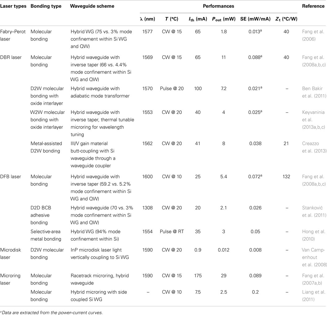
Table 1. Representative demonstrations of hybrid silicon lasers through wafer bonding technology.
Wafer Bonding Technologies for On-Chip Silicon Lasers
In general, there are two mainstreams of wafer bonding methods applying to heterogeneous integrated silicon photonics, namely the molecular bonding through interfacial bonds, and the adhesive bonding assisted with another adhesive material as bonding interface such as polymer or metal. Such wafer bonding technology is a mature process, which is widely applicable for SOI wafer fabrication, MEMS technology, and optoelectronic device fabrication. As a lot of review papers already exist (Lasky, 1986; Maszara, 1991; Tong and Goesele, 1999; Alexe and Gösele, 2004; Christiansen et al., 2006), we thus only focus the discussion on the application of hybrid silicon lasers. According to the existing demonstrations, we further summarize here the major bonding technologies as below:
(1) wafer-to-wafer (W2W) molecular bonding,
(2) die-to-wafer (D2W) molecular bonding,
(3) BCB-assisted D2W adhesive bonding, and
(4) metal-assisted adhesive bonding.
The W2W molecular bonding for hybrid silicon lasers is mainly driven by the UCSB group. Through such plasma-activated low-temperature W2W molecular bonding (Pasquariello and Hjort, 2002), they, together with their collaborators, have demonstrated various hybrid silicon lasers, starting from the first-hybrid FP laser (Fang et al., 2006), followed by racetrack-shaped laser (Fang et al., 2007a,b), DBR lasers (Fang et al., 2008a,b,c), DFB lasers (Fang et al., 2008a,b,c), MLL (Fang et al., 2008a,b,c), and multi-wavelength arbitrary waveform generation (AWG) laser (Kurczveil et al., 2011). However, for the conventional III/V-to-Si W2W bonding without thick oxide interlayer, the generated gas by-products of H2 and H2O are easily trapped inside the bonding interface and form the interfacial voids, which subsequently affect the bonding quality. In order to effectively remove such trapped gases, some proper outgas channels are designed, such as in-plane outgassing channels (IPOC) (Kissinger and Kissinger, 1993) or vertical outgassing channels (VOC) (Liang and Bowers, 2008). IPOS is formed by etching some lateral channels extended to the chip edges, so that the by-product gases can be directed to outside the bonding interface to the chip edge during post bonding annealing. However, for some close-loop structures, such as microrings, there is no way to design such IPOS. In order to solve such issue, VOC is proposed by etching some array of holes down to the BOX layer. The generated by-product gases can migrate to the closest VOC and are absorbed by SOI BOX. As both IPOS and VOC can be formed during the waveguide etching, there is no particular design requirement from the fabrication point of view. However, as the formation of such outgas channels affects the silicon layer pattern density, which will finally affect the bonding strength, it is desirable to take into account the design tradeoff between the bonding strength and the gas removal effectiveness.
Alternatively, plasma-assisted D2W molecular bonding has also been investigated for hybrid silicon lasers mainly by LETI. For large-scale manufacturability for potential massive production, the key enabling capability is the multiple dies to wafer bonding with high yield. Kostrzewa et al. (2006) first demonstrated a molecular bonding of multiple InP dies to a 200 mm silicon CMOS wafer with only 1 mm × 1 mm die size (Kostrzewa et al., 2006). For strong hydrophilic molecular bonding, both InP and silicon wafers were covered with oxide layer. Pick-and-place technology was used in order to align the InP dies to specific spots in silicon wafer, as well as to supply mechanical force to the dies through pick-and-place head. Using such D2W bonding, they demonstrated electrically pumped microdisk lasers integrated with a silicon waveguide circuit (Van Campenhout et al., 2007). However, in such D2W bonding, as the cleaning of the dies is performed ahead of the pick-and-place process, the bonding surface could be contaminated, and subsequently affecting the bonding quality and bonding yield. Furthermore, with the consideration of the pick-and-place time of 30 s/die, it takes approximately an hour for bonding 100 dies. Such long bonding time through pick-and-place process for individual die would cause the bonding surface deactivation for the molecular bonding with plasma activation.
BCB-assisted D2W adhesive bonding can address such issue with potential capability of bonding unlimited number of dies. Stanković et al. (2010) demonstrated such D2D adhesive bonding technology using BCB. The BCB is first spin-coated on silicon wafer with controlled thickness of <100 nm in order to ensure the vertical light coupling efficiency, followed with die attaching and subsequent curing at 240°C for 1 h in a nitrogen atmosphere at 1000 mbar. With the assistant of BCB adhesion, the stringent requirements of contamination-free and smooth bonding surfaces for molecular bonding are relieved significantly. Furthermore, there is, in principle, no limitation for multiple dies bonding by the assistance of BCB adhesive layer (Keyvaninia et al., 2012). Through such bonding method, various hybrid lasers, including FP laser (Stanković et al., 2011), DFB laser (Stanković et al., 2012), microring and AWG integrated multi-wavelength DBR lasers (Keyvaninia et al., 2013a,b,c), and microdisk laser (Mechet et al., 2013) have been demonstrated. However, although such adhesive bonding is with good robustness and bonding strength, the thermal dissipation could be a major problem due to the low thermal conductivity of the BCB layer. Besides, robust polymer coating process ensuring the controllable BCB thickness is also very important.
Apart from these three major bonding methods, metal-assisted adhesive bonding (Hong et al., 2010; Tanabe et al., 2010; Creazzo et al., 2013) is another one that can be used for hybrid laser integration. However, due to the potential metal contamination and the non-compatibility with the subsequent fabrication process, such as acid etching for substrate removal, the metal-assisted adhesive bonding method might not be an optimal choice for silicon heterogeneous optoelectronic integrated circuits.
In Table 2, we summarize and compare these four different bonding methods.
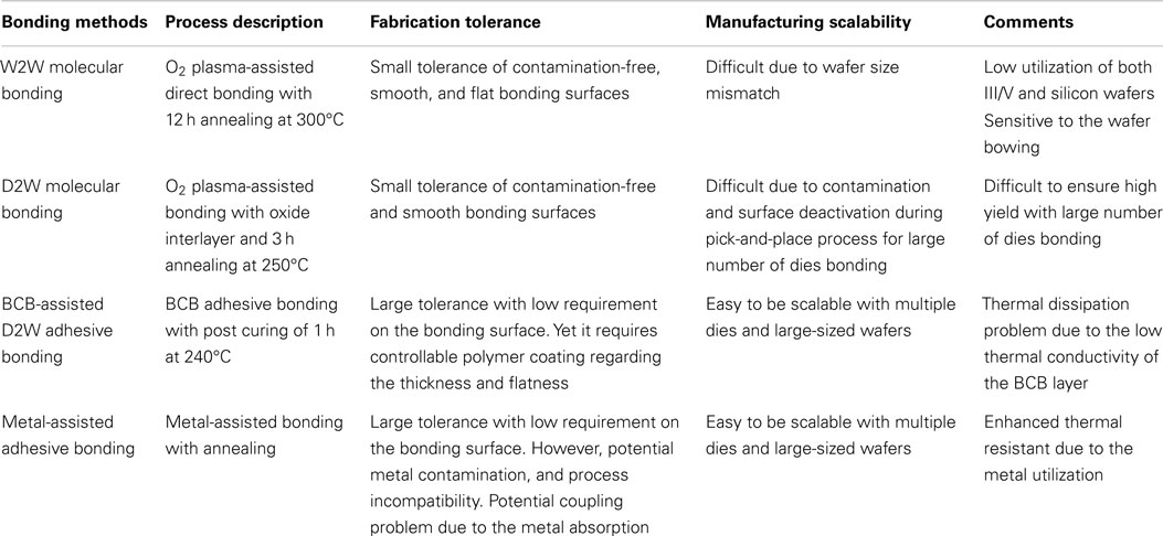
Table 2. The major bonding technology for hybrid integration.
Outline of the Manuscript
The rest of the submission is organized as follows. In the Section “III/V-to-Si Wafer-to-Wafer (W2W) Bonding Technology,” we show a demonstration of the wafer-to-wafer bonding by using low-temperature plasma-activated molecular bonding method with oxide as the bonding interlayer. In the Section “High-Throughput Multiple Dies-to-Wafer Bonding Technology,” we propose and show the demonstration of an alternative bonding technology that can perform high-throughput D2W bonding for potential massive production of silicon hybrid lasers, which is based on a batch process to simultaneously bonding all the dies to the silicon wafer. In the Section “Design of III/V-on-Si Lasers,” we provide some design guidelines of hybrid silicon laser, including the design of III/V multiple quantum wells (MQW) structures, the silicon waveguide thickness selection for hybrid laser, and the design of the vertical coupling structures. The Section “Demonstration of III/V-on-Si Hybrid Lasers” shows some hybrid silicon laser demonstrations using the bonded wafers from the proposed high-throughput D2W bonding, including FP laser, lateral-coupled distributed-feedback (LC-DFB) laser with side wall grating, and MLL. The Section “Summary and Future Outlook” summarizes this paper and addresses some of the future challenges.
III/V-to-Si Wafer-to-Wafer Bonding Technology
We have started the development of wafer bonding technology for hybrid silicon photonics integration in 2011. Considering the complete integration with existing silicon photonic integrated circuit, which consisting various silicon passive waveguide devices, high-speed modulator, and photodetectors, and are normally with thick oxide cladding, we adopt the low-temperature plasma-activated molecular bonding method (Pasquariello and Hjort, 2002) with oxide as the bonding interlayer. Furthermore, such thick cladding oxide also serves as the diffusion and absorption medium for the bonding by-products gases, thus with enhanced bonding quality and bonding yield.
For the initial development, we deposit 1.1 μm PECVD oxide on top of silicon wafers, followed with chemical mechanic polishing (CMP) to remove 100 nm oxide in order to ensure the smooth bonding interface. For all the bonding process described hereafter, we will use the similar PECVD oxide as cladding followed with CMP to smooth the bonding surface. Thus, we characterize and compare the oxide properties in terms of wafer-level uniformity and surface roughness before and after CMP. Figures 1A,B show the wafer-level oxide thickness before and after CMP. The non-uniformity is only ~1% after CMP, which suggests a very flat surface. Figures 1C,D show the AFM results before and after CMP. As deposited, the surface is relatively rough, with RMS of ~2.5 nm, while after CMP, the surface roughness is reduced significantly with RMS of ~0.4 nm, which is more suitable for wafer molecular bonding (Christiansen et al., 2006).
Figure 1. The oxide thickness (A) before and (B) after CMP. The AFM results of the wafer surface roughness (C) before and (D) after CMP.
The bonding process starts with the wafer cleaning, separately for silicon wafer and III/V wafer. First, standard SPM clean for 10 min is performed to the silicon wafer in order to remove any organic contaminants, followed with 5 min SC1 clean with megasonic to remove any particle on the surface. The III/V wafer is separately cleaned in the NH4OH solution (NH4OH:DI water = 1:15) for 1 min. Second, O2 plasma activation in a RIE chamber is performed for both silicon wafer and III/V wafer, subsequently followed with DI water rinse. These two bonded wafers are then physically contacted with each other immediately after drying and placed inside to the EVG 520 bonder for pre-bonding under N2 for 3 min with 1000 N mechanic force. After that, post bonding annealing at 300°C in vacuum is applied to the bonded pair for 12 h. Figure 2A shows the optical image of a 50 mm InP wafer bonding to a 200 mm silicon wafer before unloading from the bonder track.
Figure 2. (A) The bonded wafer before unloading from the EVG bonder. (B) The CSAM result. (C) The shear testing result. (D) The TEM results show the high-quality bonding interface.
The bonded wafers are first characterized by scanning acoustic microscope (SAM) using Sonix HS3000. Figure 2B shows the typical CSAM image for the bonded wafer. We observe that larger than 98% of the 50 mm InP area is bonded to the silicon wafer, with only limited voids, which are attributed to the particles remaining on bonding surface. Besides, the bonding quality in the wafer periphery is also not good enough, which is due to the ring-shaped imperfection of the InP wafer.
The whole wafer is then diced into 5 mm × 5 mm dies for shear testing by using a Die Shear Tester (Dage Series 4000). Figure 2C shows the extracted bonding strength, with maximum bonding strength of ~30 MPa in the wafer center region, and the averaged value of 15 MPa. We believe such bonding strength is high enough for any of the post optoelectronic fabrication process. Figure 2D shows the TEM results of the bonded wafer, which indicate a very tight bonding between InP and oxide, again suggesting a high-quality bonding.
However, although such W2W bonding has been demonstrated with high quality, there are still existing big challenges, including:
(1) insufficient III/V wafer utilization,
(2) insufficient silicon wafer utilization due to wafer size mismatch,
(3) III/V wafer global stress-induced bonding voids.
First of all, for practical application of optical interconnection, only very small portion of the silicon waveguide area needs to be bonded with III/V material for optoelectronic fabrication to form optical lasers. With whole III/V wafer bonding, most of the III/V material will be subsequently etched away during post optoelectronic fabrication. Giving such precious III/V wafers, the insufficient utilization of the III/V material results in significantly increased device cost and waste, which in turn makes it ineffectual to use the silicon photonics though it is of low cost. Second, the main stream silicon photonics has already adopted 200 mm silicon wafers. However, due to the brittleness of the InP wafers, it is very difficult to make large-sized wafers to match with silicon wafers. Although the largest available III/V epitaxial wafer can go with 150 mm, the commercially available largest-sized III/V epitaxial wafer is only 75 mm. Thus, such wafer size mismatching definitely results in the insufficient utilization of the silicon device wafer, which in turn increased the cost. Furthermore, InP wafers with multiple quantum well structures are normally with high global stress, which induces the wafer bowing. Such stress-induced wafer bowing will easily trap the air between the bonding interfaces with remained voids, thus reducing the bonding quality.
High-Throughput Multiple Dies-to-Wafer Bonding Technology
Based on the aforementioned W2W bonding method, we propose an alternative proprietary high-throughput multiple D2W bonding method, which is based on temporarily bonding III/V dies to a handle silicon wafer through pick-and-place process for simultaneous batch processing. Such high-throughput multiple D2W bonding method is the key enabling technique for potential manufacturability of large-scale hybrid optoelectronic integrated circuit (H-OEIC).
Figure 3 shows the key process steps of the proposed multiple D2W bonding technology, which includes:
(a) the programmable reconfiguration of III/V dies onto a handle wafer via pick-and-place process,
(b) the D2W bonding through the notch alignment between the two 8″ wafers, after batch processing of wafer cleaning and plasma activation, and
(c) the dies releasing from the handle wafer and transferring to silicon device wafer.
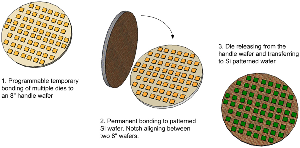
Figure 3. Illustration of the key processing steps of the multiple D2W bonding technology.
The most critical step here is the choice of the adhesion layer for the temporary III/V dies bonding to the handle wafer, which includes the following two trade-off considerations.
(1) The adhesion should be strong enough to stick the III/V dies on the handle wafer without peeling off during the subsequent III/V dies batch processing, including InGaAs cap layer wet etching, pre-clean, wafer drying, and plasma activation, etc.
(2) The adhesion should not be excessively strong so that the III/V dies can be successfully released and transferred to the Si device wafer after pre-bonding.
The programmable reconfiguration of the dies onto the handle wafer is realized through pick-and-place process by pre-determining the position coordinates of each die with considering the wafer-level silicon device die distribution. Unlike the pick-and-place process in flip-chip bonding, which directly bonds the dies to the actual wafer (Kostrzewa et al., 2006), the pick-and-place in our proposed method only helps to distribute the dies onto a handle wafer without flipping the chips. Thus, all the dies attached to the handle wafer can be simultaneously performed with different process steps for wafer bonding, such as InGaAs cap layer etching, wafer clean, and plasma activation.
The D2W bonding alignment accuracy is mainly determined by the notch alignment, which is performed manually and induces a relatively large misalignment of ±500 μm, compared to the misalignment of only ±5 μm from the programmable reconfiguration by pick-and-place process. However, as the alignment of the III/V devices to the silicon waveguide device is determined through photolithography during optoelectronic fabrication process after wafer bonding, such misalignment can easily be compensated by adopting relatively large-sized III/V dies.
Figure 4 schematically illustrates the detailed bonding process flow starting from the preparations of silicon and III/V wafer. For either blanket silicon wafer or patterned silicon wafer with photonic devices, the wafers are cladded with PECVD oxide, followed with CMP process to smooth the bonding surface. As the hybrid laser performance is largely dependent on the vertical coupling efficiency, which is determined by the inter-layer oxide thickness, it is of very importance to control the oxide thickness by CMP process.
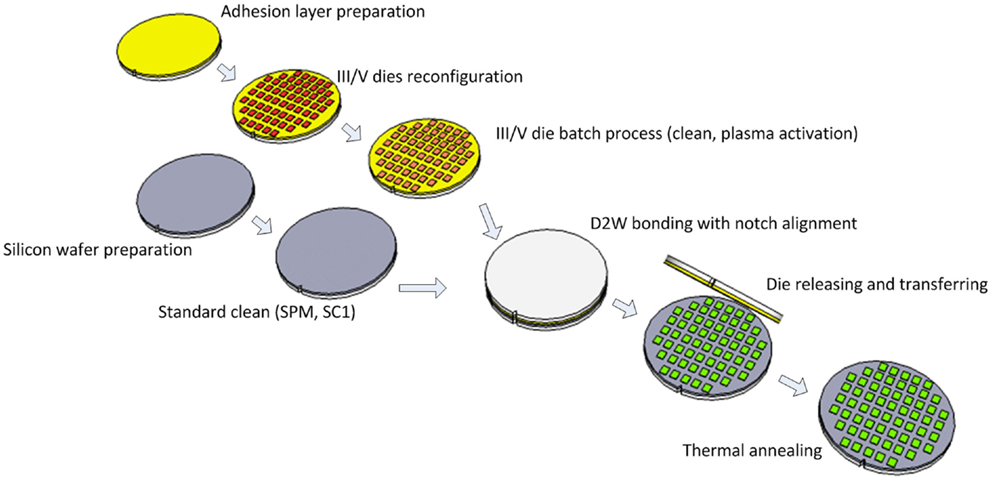
Figure 4. The fabrication process flow of the multiple D2W bonding technology. The process includes two different folds, i.e., the bonding wafers preparation including the III/V dies adhesion to handle wafer for batch process and the silicon device wafer fabrication, and D2W bonding through dies releasing from handle wafer and transferring to silicon device wafer.
The preparation of the III/V dies includes the III/V wafer dicing into certain sized dies, the preparation of the adhesion layer to the handle wafer, and the programmable reconfiguration of the III/V dies temporary bonding to the handle wafer through pick-and-place process. Typically, the mechanical wafer dicing will result in edge roughness along the dicing lane, thus subsequently cause the low quality bonding near the die periphery. Besides, such dicing process may also introduce particles to the wafer surface cause contamination. Thus, a sacrificial InGaAs cap layer in order to protect the III/V bonding surface is designed in our demonstration. The applied mechanic force by the pick-and-place head also needs to be well controlled in order to ensure the successful die releasing from the handle wafer after pre-bonding. Due to the direct contact of the pick-and-place head, the die surface could be contaminated. However, owing to the sacrificial InGaAs layer, the bonding surface can be well protected without contamination or surface damage. We have checked and compared the surface condition of the III/V dies before and after the etching of the sacrificial InGaAs layer. We observe the particles on the chip surface after the wafer dicing and pick-and-place process, which is with relatively high RMS of 0.198 nm. In comparison, after the etching of InGaAs cap layer, the surface roughness is improved with reduced RMS of 0.182 nm, which is far below the required RMS of <1 nm for wafer direct bonding (Christiansen et al., 2006).
Prior the physical contact of the wafers for molecular bonding, the silicon wafer is performed with standard SPM clean for 10 min and SC1 clean with mega sonic for 5 min, while III/V die-attached handle wafer is first performed with sacrificial InGaAs cap layer etching in H3PO4 solution for 1 min, followed with standard clean in NH4OH solution for 2 min. After that, O2 plasma activation is applied to both silicon wafer and III/V dies in a RIE chamber for 1 min, followed with DI water rinsing and wafer drying. The III/V dies and the silicon wafer are then physically contacted with each other by notch alignment between two 8″ wafers, followed with pre-bonding in the 200 mm EVG bonder for 2 min with 1000 N mechanical force applied. The III/V dies are released from the handle wafer after pre-bonding, and all III/V dies are now transferred to the silicon device wafer. Finally, the bonded pairs are placed back to the EVG bonder for post-bonding annealing at 300°C for 12 h.
As a proof-of-concept demonstration, we show here the bonding of 104 InP dies to an 8″ silicon wafer. The silicon wafer is covered with 1 μm PECVD oxide after CMP. The InP dies are diced into 5 mm × 5 mm in size. Figure 5A shows the photo image of the bonded wafers with nearly all InP dies are successfully bonded to the silicon wafer. The only missing piece is peeled off during pick-and-place process. The CSAM shown in Figure 5B suggests a successful bonding. The dark areas, which suggest less strong bonding, come from the dies located in the InP wafer edge. Figure 5C shows the sheer testing results. The maximum bonding strength is larger than 20 MPa, with an averaged bonding strength of ~13 MPa, which is comparable with that of W2W bonding under the same process.
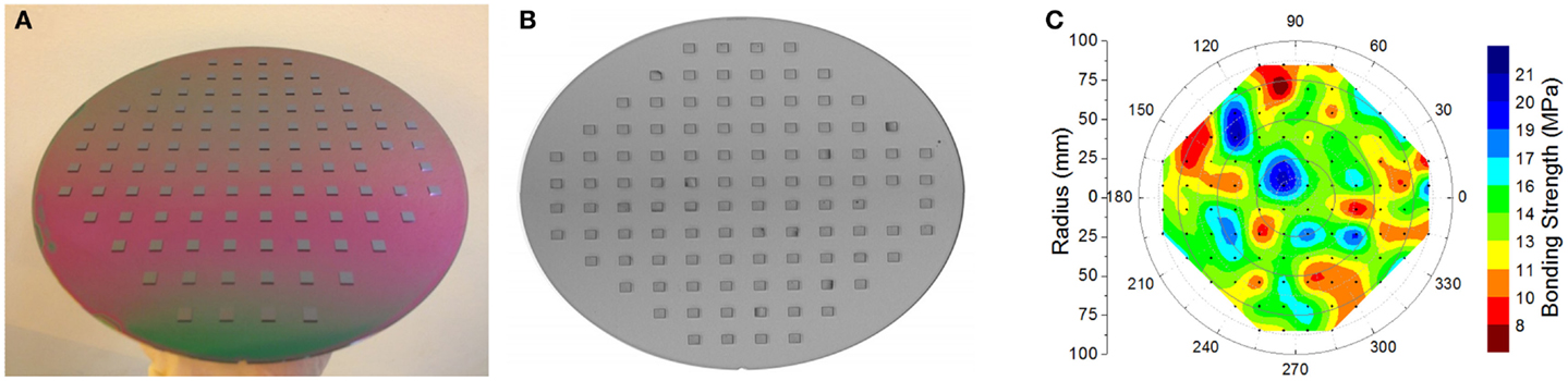
Figure 5. Demonstration of 104 III/V dies bonding to silicon wafer. (A) Photo image of the bonded wafer, (B) CSAM results, (C) shear testing results.
All in all, we believe that there are at least two significant implications of the proposed multiple D2W bonding technology:
(1) The significantly increased bonding efficiency owing to the simultaneous batch process. Through the batch process of the III/V dies (pre-clean, plasma activation, etc.), it is possible to bond unlimited number of dies. It also helps to avoid potential contamination by performing the pick-and-place before cleaning process, and eliminates the time link constraint of the bonding surface deactivation. This is the most significant processing advantage comparing to the conventional pick-and-place method.
(2) The scalability to whatever-sized silicon wafers. Such multiple D2W bonding technology can easily be adopted for even larger-sized silicon wafers, such as 300 mm wafer. This is the most critical step toward the potential manufacturability of H-OEIC.
Design of III/V-on-Si Lasers
A hybrid III/V-on-silicon laser consists of a III/V epitaxial-layered structure and a silicon waveguide. It is a device that emits laser beams from silicon waveguides by electrical/optical injection to the III/V region. In this section, we will discuss the design of hybrid III/V-on-silicon lasers with regard to two fundamental laser elements, namely, optical gain medium and optical waveguide cavity.
Design of III/V MQW Structures
There are two main material systems for the fabrication of long-wavelength lasers emitting at 1.55 μm, which are InGaAsP/InP and InGaAlAs/InP systems. Both kinds of materials can be used to fabricate hybrid lasers. InGaAlAs MQWs exhibit a larger conduction band discontinuity (Ec = 0.72Eg), and smaller valence band discontinuity compared with InGaAsP MQW. This leads to an improved electron confinement, which can improve the temperature characteristics of semiconductor laser diodes. Thus, InGaAlAs/InP material system is more suitable for high speed and uncooled operation of semiconductor laser diode. In this study, we select this material system for the hybrid silicon lasers demonstration. The MQW region includes eight Al0.055Ga0.292In0.653As quantum wells separated by nine Al0.055Ga0.292In0.653As barriers. The gain spectrum of the MQW is calculated and the wavelength of peak gain is designed at 1550 nm when the carrier injection density increases from 5 × 10¹⁷ to 5 × 10¹⁸/cm3 as shown in Figure 6A. Figure 6B shows the measured photoluminescence (PL) spectrum for III/V epitaxial wafer at room temperature with the peak wavelength at about 1550 nm.
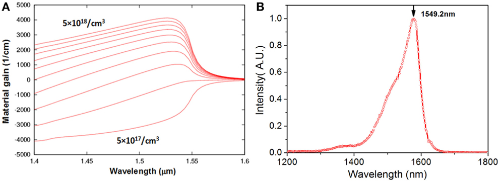
Figure 6. (A) The calculated gain spectrum under different carrier injection concentration. (B) The measured photoluminescence (PL) spectrum for III/V epitaxial wafer.
Design of Hybrid Laser Vertical Waveguide Structure
As mentioned, the optical gain comes from overlying III/V stack layer, which needs to be structured to efficiently inject electrons or holes into the MQW regions. A high overlap between the optical mode and the MQW benefits to achieve a high optical gain, which means that the optical mode needs to be well confined in the III/V waveguide. However, on the other hand, the light has to be confined sufficiently inside the silicon output waveguide for the efficient light extraction. In view of this, there are mainly two kinds of waveguide structures considering the optical power distribution for the hybrid laser with optical mode predominantly confined either in the silicon waveguide or in the III/V overlay. This leads to two different optical cavity designs. In the first design, the optical cavity comprises both III/V and silicon waveguides and the mode is mainly guided within the Si waveguide and evanescently coupled with the III/V waveguide. Such structure is also called as overlapped structure with hybrid mode (Fang et al., 2006, 2007a,b, 2008a,b,c, 2009). It has the advantage of making the coupling to a passive silicon waveguide straightforward and wavelength selective features can easily be defined in the silicon waveguide layer using CMOS fabrication techniques, which provides an accurate mechanism to control the emission wavelength of the laser. However, it requires a controllable thin bonding layer (<50 nm) for efficient optical coupling, which may increase the difficulty of bonding process. Furthermore, due to the weak interaction between the optical mode and gain material, it usually requires longer laser cavity, and thus resulting in high power consumption. In the second design, the mode in the hybrid section is mainly guided by the III/V waveguide, and the light is coupled from the III/V waveguide to the silicon waveguide through waveguide mode transformer, such as inverse tapers (Yariv and Sun, 2007; Sun et al., 2009a; Ben Bakir et al., 2011). In such design, the bonding interface can be relatively thick (typically from 30 to 150 nm) due to the released coupling constrain for the bonding interface. The advantage is that the optical mode experiences a high optical gain in the central region of the laser structure. However, the challenge of this structure is the fabrication of low-loss tapered waveguides. Hereafter, we name such design as adiabatic tapered coupling structure.
Silicon waveguide thickness selection
The selection of the silicon waveguide thickness depends on the detailed device dimensions/structures and the fabrication process. For indium phosphide (InP)-based gain waveguides, the effective refractive index is typically larger than 3.2 if the waveguide width and height are larger than 1 μm. In order to achieve this index for silicon waveguides for effective coupling with the InP-based gain region, the corresponding silicon waveguide thickness needs to be sufficiently large. Figure 7 shows the calculated effective refractive index of the fundamental mode in silicon waveguide depending on the waveguide thickness. It indicates that the required silicon thickness needs to be larger than 450 nm to achieve an effective index of 3.2 for the waveguide with 2 μm in width. Such thick silicon layer does not match with the current mainstream silicon photonics. However, on the other hand, it is still possible to couple light from 220 nm silicon to InP waveguides by using very narrow InP waveguides (~200 nm) to push down the value of effective index, although the fabrication is difficult to form these narrow InP waveguides by conventional photolithography.
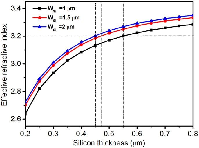
Figure 7. Effective refractive index of the silicon waveguide fundamental mode as the function of silicon waveguide thicknesses. Both top and bottom claddings are oxide (n = 1.45) and silicon index is chosen as 3.48 at the wavelength of 1550 nm.
Overlapped structure with hybrid mode
As mentioned above, there is a tradeoff between the optical mode confinement in the III/V and silicon regions for the overlapped structure. The bonded III/V-Si structure forms the hybrid waveguide cavity. The effective refractive index of III/V active and Si regions are critical parameters for the hybrid waveguides, which, respectively, determine the light confinement factors in III/V and Si region. In our design, the confinement factors over the silicon and the quantum well regions are modified by altering the silicon waveguide thickness and the separate confinement heterostructure (SCH) thickness in order to ensure sufficiently low-threshold gain for lasing. While the thicker silicon waveguide pulls the optical mode into the silicon layer, the larger SCH thickness can drag back the optical mode into the III/V region.
Figure 8A shows the calculated optical confinement factors in MQW and Si depending on the Si waveguide width under different Si thickness, with assuming the III/V ridge width and the SCH thickness of 6 μm and 250 nm, respectively. It shows that when the waveguide widths of III/V and Si are fixed, the optical confinement in Si waveguide can be increased by using a thick Si layer. With the silicon waveguide thickness of 700 nm, large confinement of up to 70% in silicon waveguide is achieved. However, the device performance is very sensitive to the bonding interface quality due to the overlapping of the optical mode with the bonding interface between the III/V and the silicon. Based on the analysis, we adopt silicon thickness of 500 nm for the demonstration of hybrid Si lasers.
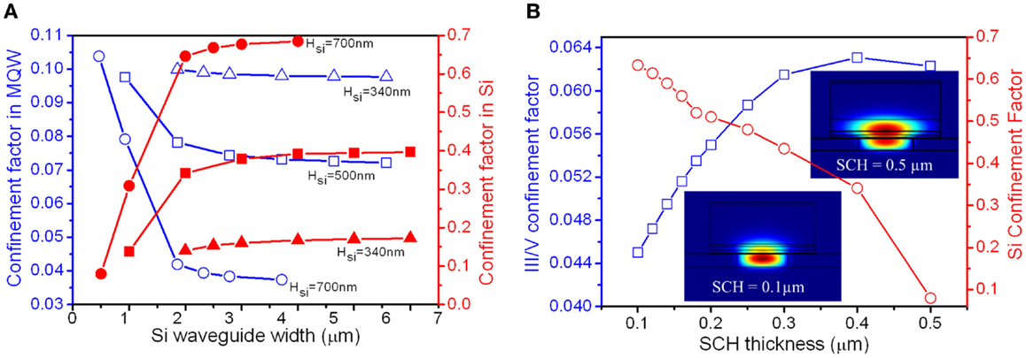
Figure 8. Confinement factor of optical mode in multiple quantum wells (MQW) and Si waveguide as a function of (A) the Si waveguide width under different Si waveguide thicknesses, and (B) the SCH thickness. Insets: the simulated field distributions of the fundamental TE mode with different SCH thicknesses. It shows that by increasing the thickness of SCH layer up to 500 nm, the optical mode is more confined in the III/V active layer.
Figure 8B shows the simulated optical confinement factor in MQW and in silicon waveguide with different SCH thickness, with the fixed III/V and Si waveguide widths of 4 and 2 μm, and Si waveguide thickness of 500 nm. As the SCH thickness increases, the optical mode confinement in III/V region increase, which in turn significantly decreases the optical mode confinement in silicon waveguide. Inserts in Figure 8B show the simulated field distributions with SCH thicknesses of 0.1 and 0.5 μm. It shows obviously that for the small SCH thicknesses, the optical mode lies primarily in the silicon region, while the optical mode is dragged into III/V region with increased SCH thickness. The ability to control the optical mode with the SCH thickness is a key feature of this platform. For hybrid lasers, higher optical confinement is needed to achieve lower threshold current. Thus, we choose an optimized SCH thickness of 0.18 μm for the hybrid lasers.
For such hybrid III/V-on-silicon lasers, another challenge arises from the control of the bonding layer thickness. Generally, a thin bonding layer (<50 nm) is needed for efficient optical coupling between III/V and silicon regions, while the thicker bonding layer benefits to the bonding quality of III/V layer and the bonding yield improvement. For direct bonding without oxide interlayer, it is easy to achieve such thin thickness, which is usually only the native oxide. However, this process is particularly sensitive to surface roughness and particles contamination, which would limit the bonding quality and bonding yield. DVS-BCB bonding can be used for the heterogeneous integration of III/V material on silicon to improve the yield. However, it is difficult to obtain a controllable thin bonding interlayer of <50 nm. In our case, we choose silicon oxide as interlayer between III/V and silicon, which is also compatible with the mainstream silicon phonics, in which all the devices are with oxide cladding.
Figure 9A shows the calculated optical confinement factor in MQW and silicon waveguide as the function of interlayer oxide thickness. In the simulation, we assume the fixed silicon thickness of 500 nm, the silicon waveguide width of 3 μm, and III/V ridge waveguide with of 6 μm. We observe from the results that the Si confinement factor largely decreases when the interlayer thickness increases from 10 to 100 nm. Only approximately 5% optical light is confined in the silicon waveguide when the interlayer thickness is 100 nm.
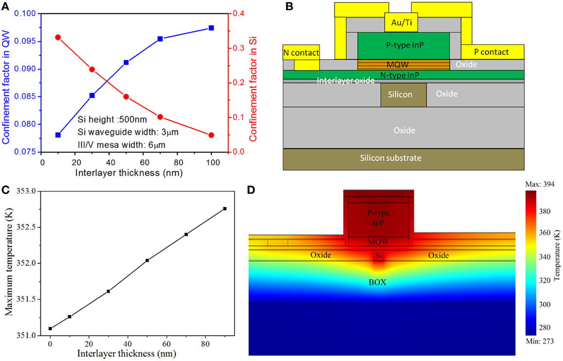
Figure 9. (A) The confinement factor of the optical mode in the MQW and silicon layers, respectively, as a function of the interlayer thickness. (B) The simulation structure of the thermal distribution. (C) The temperature changes in the III/V active region with regard to the oxide interlayer thickness. (D) The simulated thermal distribution with the interlayer thickness is 0 nm.
Additionally, the interlayer of oxide at the bonding interface also affects the characteristics temperature of hybrid III/V-on-silicon laser due to the poor thermal conductivity of as low as 1.3 W/m/K. The modal gain of laser is dependent on the temperature of the active region. As the temperature of active region increases, the modal gain decreases due to the increased carrier leakage out or not reaching the active region, and/or increased non-radiative recombination. The decrease of modal gain leads to high threshold current and low output optical power. In order to investigate the effect of interlayer on the thermal characteristics of the hybrid lasers, a two-dimensional model of the device structure is conducted using COMSOL by mapping out the heat dissipation of each layer. Figure 9B shows the simulation structure. In the simulation, the structure parameters are as follows: III/V ridge width, Si ridge width and thickness, and the laser cavity length are assumed to be 6 μm, 1 μm, 500 nm, and 1000 μm, respectively. Injection current is 500 mA and the corresponding voltage is 4 V. Figure 9C shows the calculated working temperatures in the III/V active region with different thicknesses of the oxide interlayer. The increase of temperature in the III/V active region versus interlayer thickness is about 0.02 K/nm. For illustration purpose, Figure 9D shows as an example the thermal distribution within the layered structure for the oxide interlayer thickness of 0 nm. The thermal distributions for the other thicknesses are similar. Actually, we can conclude from the study that the main hurdle for the heat dissipation is the SOI BOX layer, which can be seen from the results without oxide bonding interlayer (thickness = 0 nm). Thus, for enhanced thermal management, novel designs such as thermal shunt (Liang et al., 2012) are required to effectively remove the generated heat.
Adiabatic tapered coupling structure
For the adiabatic tapered coupling structure, the mode in the hybrid section is mainly guided by the III/V waveguide, and the light is coupled from the III/V waveguide to the silicon waveguide through a tapered waveguide. It shows that a tapering length ~100 μm is required for a sufficient light coupling with minimized optical loss. By using such tapered coupling, it eliminates the tricky tradeoff between the modal gain and vertical coupling efficiency, which is inherent in the overlapped waveguide structures. Therefore, hybrid lasers with a short cavity as pure III/V laser are possible. Up to now, the hybrid lasers with the high performances are achieved using such tapered coupling scheme (Levaufre et al., 2014; Zhang et al., 2014).
In order to efficiently couple the light between the Si-III/V hybrid waveguide and the silicon waveguide, the III/V waveguide and silicon waveguides are tapered simultaneously in the same direction. Here, we adopt a three-dimensional approximated model based on beam propagation method (BPM) in order to optimize the tapering structure of the silicon waveguide and III/V waveguide for an efficient coupling. Figure 10A schematically illustrates the design of such waveguide tapering structure. The coupling efficiency largely depends on the tapering design, especially the III/V waveguide taper width and taper length. Here, we simulate such dependency by varying the taper width and taper length, while fixing the III/V waveguide width of 5 μm, the silicon waveguide width of 1 μm, and the silicon taper length of 100 μm.
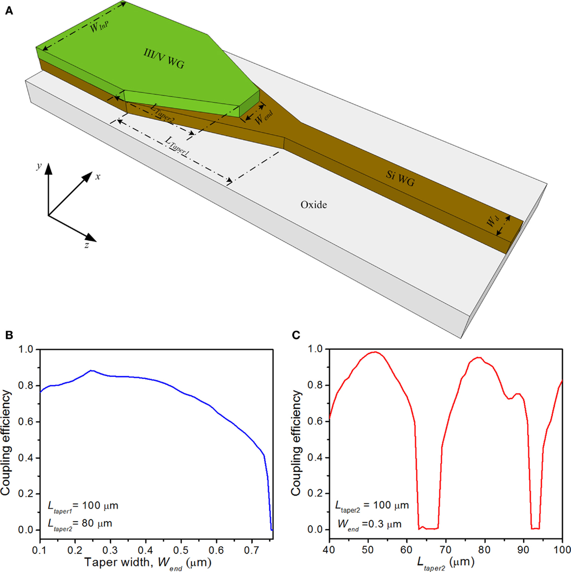
Figure 10. (A) Schematics of the tapering structure for the vertical coupling between III/V waveguide and silicon waveguide. WInP: III/V waveguide width, Wend: III/V waveguide taper width, Wd: silicon waveguide width, LTaper1: silicon waveguide taper length, LTaper2: III/V waveguide taper length. The whole structure is cladded with oxide. Coupling efficiency of III/V waveguide to Si waveguide as functions of (B) the III/V waveguide taper width, and (C) the III/V waveguide taper length.
Figures 10B,C, respectively, show the simulated coupling efficiency from III/V-Si hybrid waveguide to silicon waveguide as functions of the III/V waveguide taper width and tape length. It suggests that the coupling efficiency from III/V-Si hybrid waveguide to Si waveguide can be as high as 85% by using an 80-μm-long III/V waveguide taper and a 100-μm-long silicon waveguide tape. Through optimizing the III/V waveguide taper width and III/V waveguide taper length, the maximum coupling efficiency can be as high as 99%. However, due to the optoelectronic fabrication limitation, we are not able to demonstrate the hybrid laser using such adiabatic tapered coupling structure.
Demonstration of III/V-on-Si Hybrid Lasers
Using the proposed multiple D2W bonding technology, we have demonstrated various hybrid silicon lasers, including FP lasers, DBR lasers, sidewall-grating lasers, racetrack-shaped microring lasers, and MLL. In this section, we will first introduce the hybrid silicon laser fabrication process, leveraging on IME’s CMOS-compatible silicon photonic fabrication facilities and NTU’s expertise in optoelectronics fabrication capability, followed with showing some hybrid silicon laser demonstrations as the examples.
III/V-on-Si Hybrid Laser Fabrication Process
The III/V-on-Si hybrid laser fabrication in our demonstrations includes two parts, namely silicon passive device fabrication using IME’s CMOS line and multiple D2W bonding in IME’s MEMS line, and III/V optoelectronics fabrication in NTU. Figure 11 shows the fabrication process flow. We adopt commercially available SOI wafer with 340 nm silicon layer sitting on a 2 μm buried oxide (BOX) layer. The fabrication starts with the blanket silicon epitaxy to ~500 nm for refractive index matching between silicon waveguide device and InP gain medium. After the deposition of 70 nm oxide as the hard mask, the waveguide structures, including both grating coupler and inverse taper coupler are patterned by deep UV photolithography and transferred onto the silicon layer by using deep RIE etching. For the grating coupler, the silicon etching thickness is 377 nm. While for other waveguide devices, second silicon etch is applied down to the BOX layer by covering the surface grating coupler area with additional photo resist. Oxide cladding of 650 nm in thickness is deposited followed by a surface planarization step, which includes oxide etch-back with 500 nm in depth and CMP process. Such planarization steps with CMP also help to smooth the bonding surface with very small surface roughness for molecular bonding. The interlayer oxide thickness can be well controlled by the CMP process, with only ~50 nm oxide left atop the silicon waveguide in our demonstration. For enhanced flatness and uniformity of the bonding surface, we only etch away the silicon surrounding the devices, remaining most of the silicon areas forming silicon plateaus.
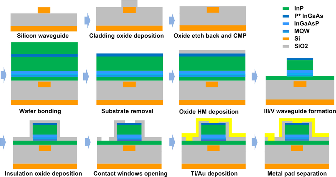
Figure 11. The fabrication process of the hybrid silicon laser in a ridge waveguide structure.
The multiple D2W bonding is then performed after the preparation of III/V dies, followed with the process described in Section “III/V-to-Si Wafer-to-Wafer (W2W) Bonding Technology.” As the designed devices are all within an area of 8 mm × 8 mm, the InP dies are all diced with 9 mm × 9 mm with the consideration of bonding misalignment of ±500 μm for the notch alignment, thus ensuring the full covering of all the silicon photonic devices within the III/V die area. For a 50 mm InP wafer, there are only 16 full dies with 9 mm × 9 mm in size. Thus, for the purpose of hybrid silicon laser demonstration using such D2W bonding technology, we only perform 16-dies bonding to 200 mm silicon wafers, with some of the silicon photonics device area being wasted. Figure 12A shows the photo image of the 16-dies bonded silicon wafer. Figure 12B shows the CSAM results. Except some particle-induced bonding defects, all the dies are bonded very well. However, we clearly observe that some of the die edge periphery regions are not bonded well due to the wafer dicing induced damage. Figures 12C,D, respectively, show the TEM and cross-SEM of the bonding structures, both suggesting very reliable bonding quality.
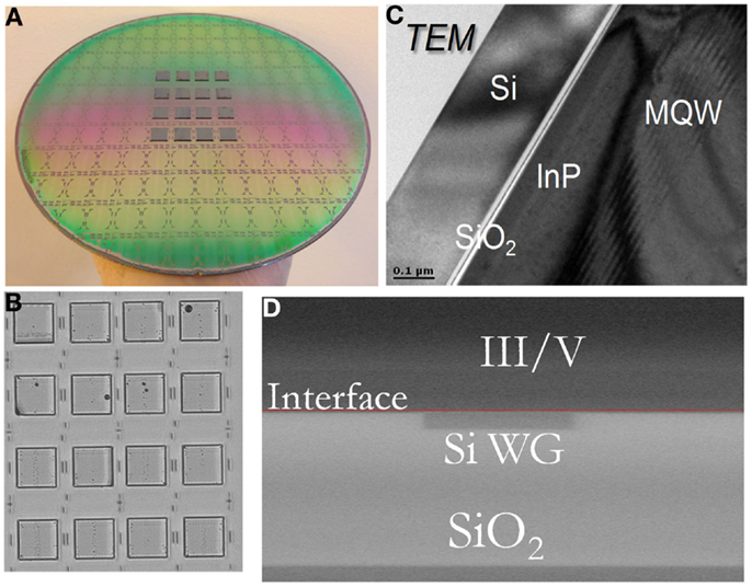
Figure 12. (A) The optical image of the 16-dies bonded silicon wafer. (B) CSAM results. (C) TEM of the bonding structure. (D) Cross-SEM of the bonding structures.
The III/V optoelectronic fabrication starts from the InP substrate removal using HCl solution. After photolithography, the InP mesa structures are formed by using H3PO4, H2O2, and HCl mixed solution to etch the InGaAs contact layer and p-InP cladding layer. The SCH layer and QW layer are also etched using H3PO4:H2O2:H2O solution, stopping on the n-InP cladding layer. Then, an SiO2 insulator layer with the thickness of 300 nm is deposited, followed with the contact opening for p-type and n-type injection by one-time photolithography and the oxide is etched by HF solution. After that, Ti/Au metal contacts are formed by sputtering, with wet etching to form a Ti/Au slot between the n-type and p-type contacts using diluted HF and KI solution, respectively.
Fabry–Perot Lasers
The CW operation of the optical laser requires good thermal management to remove the generated heat. In the case of FP lasers, another way is to design narrow ridge waveguide to generate less heat. In our demonstration, we design a FP laser with ridge waveguide width of 6 μm. The laser facets are formed by lapping down the Si substrate to around 60 μm, followed with mechanical cleaving. The length of the FP laser is ~720 μm. The demonstrated FP laser is able to work at room temperature with CW operation. Figure 13A shows the measured P–I curves under different temperatures. The threshold current at 264 K is ~45 mA, and increases significantly to ~100 mA at room temperature. We attribute such fast increase of the threshold to the thick oxide interlayer, which prohibits the heat dissipation efficiently. The measured output power from a single facet without any reflection coating is more than 1 mW. This includes the coupling loss due to the un-optimized testing setup for light collection, which is estimated only with ~20% light collection efficiency. The thermal dissipation is very important for CW lasing. Figure 13B shows the measured lasing spectra under different temperatures. The wavelength shift with temperature is about 0.75 nm/K.
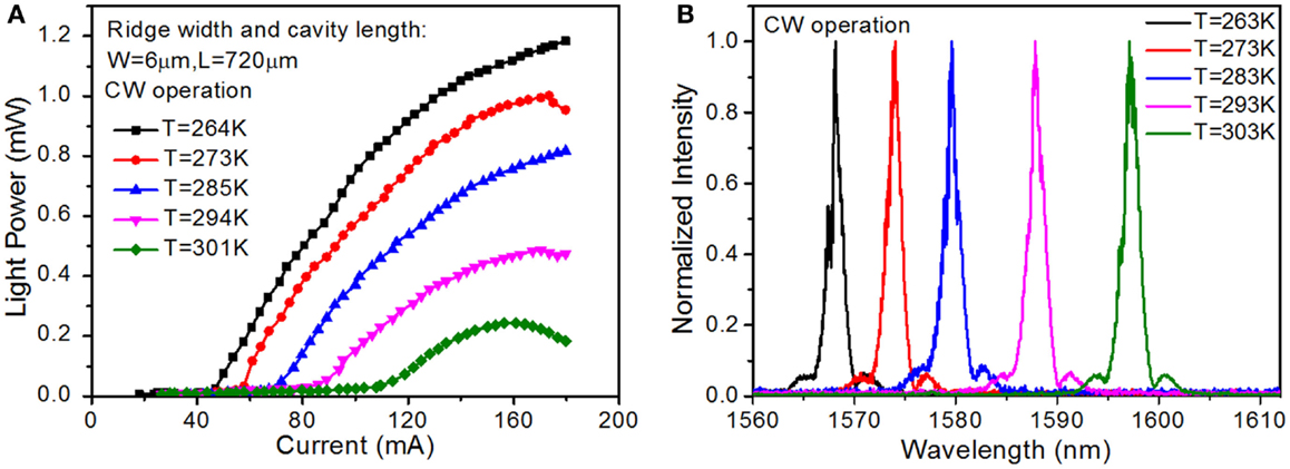
Figure 13. (A) The power–current characteristic curves and (B) the lasing spectra of a typical hybrid silicon FP laser measured under different temperature.
Lateral-Coupled Distributed-Feedback Lasers with Side Wall Grating
The FP laser is fabricated by lapping down the silicon substrate and mechanical cleaving to form the facets. From the optical communication and optical interconnect applications point of view, such FP lasers are not practical for photonic integration. Furthermore, how to achieve good facet is still a main challenge and a key limiting factor for high-performance hybrid lasers as reflection coating is always required in order to optimize the cavity transmission and reflection. In view of this, optical resonators, Bragg grating structures that form the cavities through fabrication are the good candidates for on-chip hybrid laser. We here show as an example of a hybrid laser using LC-DFB structure as the laser cavity.
Figure 14A schematically shows the perspective view of the LC-DFB hybrid laser with illustration of the key parameters, including the Bragg grating period Λ, the silicon ridge width D, and the grating teeth width, W1. Considering the fabrication limitation, we design third-order later Bragg grating in order to achieve single-mode operation. With regard to the silicon thickness of 500 nm, the grating period Λ is 670 nm with filling factor of 0.5. The ridge width D and the teeth width W1 are, respectively, designed with 2 and 1 μm. The Bragg grating is centered beneath the III/V gain region, which is with the width of 12 μm. Both LC-DFB structure and III/V gain region are designed with the same lengths. In order to extract the output laser light for easy characterization, the vertical grating couplers are adopted. For the vertical grating coupler, the period is designed to be 640 nm with filling factor of 0.5, and the silicon etch depth is 377 nm. Such grating coupler design is purely based on theoretical calculation, without any process verification and optimization. For this demonstration, we did not design any mode transformer between III/V layer and silicon waveguide layer, thus expecting some transition loss. Figure 14B shows the optical microscope image of the fabricated hybrid LC-DFB laser with integrated vertical grating couplers. The LC-DFB structure and the III/V gain region are designed with same length of 700 μm, while the silicon device including two grating couplers is ~2750 μm. Due to the optoelectronic fabrication limitation, there is no designed taper between III/V waveguide and silicon waveguide, thus expecting relatively high transition loss. Figures 14C–E show the SEM images of the fabricated LC-DFB and vertical grating coupler, while Figure 14F shows the cross-sectional SEM of the vertical structures, illustrating the Si waveguide, the III/V layer, and the Ti/Au layer.
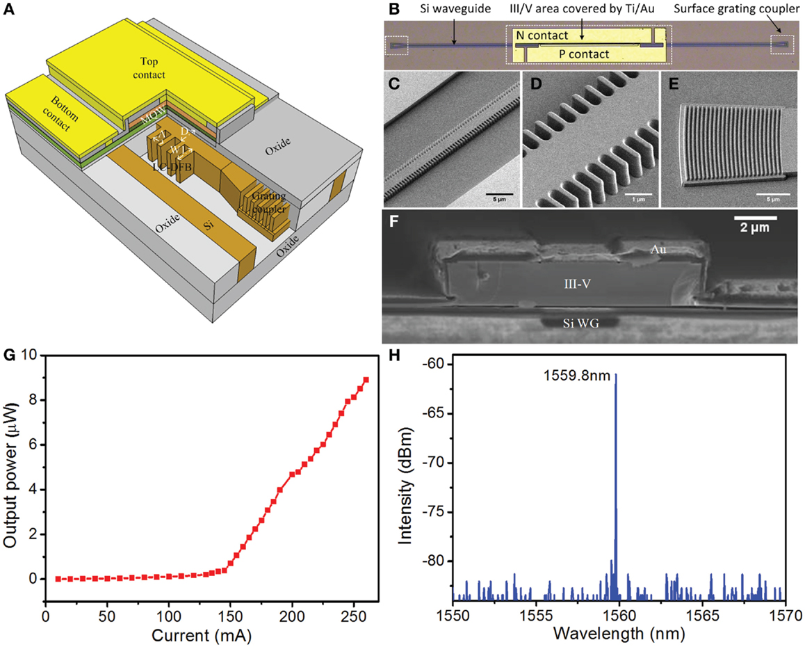
Figure 14. (A) The perspective view of the hybrid LC-DFB laser integrating with surface grating coupler, with illustration of the key design parameters. Λ: grating period, D: the ridge width, and W1: the grating teeth width. (B) Top-view optical microscope image of a LC-DFB hybrid laser integrated with vertical surface coupler. (C–E) The SEM of the LC-DFB structures and the grating coupler. (F) The cross SEM of the vertical layered structure. (G) The light power output and (H) the laser spectrum of the hybrid silicon laser with sidewall Bragg grating structure. The output power is directly measured from the surface grating coupler.
Figures 14G,H show the measured P–I curve and the spectrum of the LC-DFB hybrid laser under pulse operation. The threshold current is ~120 mA, corresponding to a threshold current density of ~1.42 kA/cm2. From the spectrum, we see clearly single-mode operation with the peak wavelength at 1559.8 nm and a side-mode-suppression ratio (SMSR) larger than 20 dB. This is expected from the LC-DFB design. However, the maximum output power is only ~10 μW upon 250 mA current injection, which also can be observed from the spectrum measurement. We attribute the relatively low output power to the following two reasons, namely, the accumulated optical loss, and the inefficient vertical light coupling. First of all, the optical loss, which mainly includes the surface grating coupler coupling loss, the Bragg grating scattering loss, and the non-radiative recombination loss from the bonding interface, affects the light output significantly. From the reference measurement for the device only with passive silicon waveguide yet bonded III/V layer, the accumulated total loss is >40 dB, which is mainly due to the unoptimized surface grating coupler. Second, the oxide interlayer in our design, which might not be able to control precisely, will affect the light coupling efficiently from III/V layer to silicon waveguide. Furthermore, the polarization sensitivity of the surface grating coupler can also induce additional optical loss. Thus, the optimized grating coupler design for the light extraction from the silicon waveguide and the vertical light transition structure for light coupling from III/V layer to silicon waveguide can significantly increase the laser output power. Besides, by optimization of the Bragg grating period and silicon waveguide thickness, the SMSR can also be enhanced.
Passively Mode-Locked Lasers
Semiconductor MLLs are excellent candidates for generating stable ultra-short optical pulses, which have a corresponding wide optical spectrum of phase correlated modes and high repetition rate. Optical frequency combs emitted by MLLs can have high extinction ratios, low jitter, and low chirp, which can be utilized in a variety of applications including AWG, optical clock generation and recovery, coherent communications systems, high-speed analog-to-digital conversion (ADC), and optical time-division multiplexing (OTDM), etc. Integration of MLLs on silicon is very promising as it combines the low-loss and low-dispersion characteristics of silicon material with high gain III/V material, thus ensuring improved performance. Furthermore, it will be possible for semiconductor MLLs to generate ultra-short optical pulses with low repetition rate on the silicon platform owing to the long cavity length. Here, we show our preliminary demonstration of a passive MLL using the developed heterogeneous integration platform.
The optical cavity of the MLL is defined by a 1250-μm-long gain section, a saturable absorber (SA) with the length of 30-100μm, and cleaved facet at the waveguide end. The gain section and SA are separated by a 20 μm electrical isolation region with isolation resistance >1 kΩ. The SA is made up of the same active material as the gain section. The difference between the SA and gain section is that SA absorbs the light in the cavity upon applying a reverse bias, while the gain section amplifying light upon forward current injections.
The laser optical output is collected by a photodiode located in front of the cleaved facet. The typical threshold current with an unbiased 50-μm-long SA section is 88 mA. The device has a maximum single facet CW output power of 1 mW at room temperature when the injection current is 140 mA. The series resistance is about 8.5 Ω, while the slope efficiency is about 0.02 mW/mA. Figure 15A shows the measured optical spectra at different injection currents. It shows that the widest optical emission is centered at about 1605 nm with a full-width at half-maximum (FWHM) of 5.4 nm at the injection current of 110 mA measured by an optical spectrum analyzer (OSA). Assuming the generated optical pulse is chirp-free and the shape of the pulse is with a Sech-function, the width of the optical pulse is calculated to 0.5 ps.
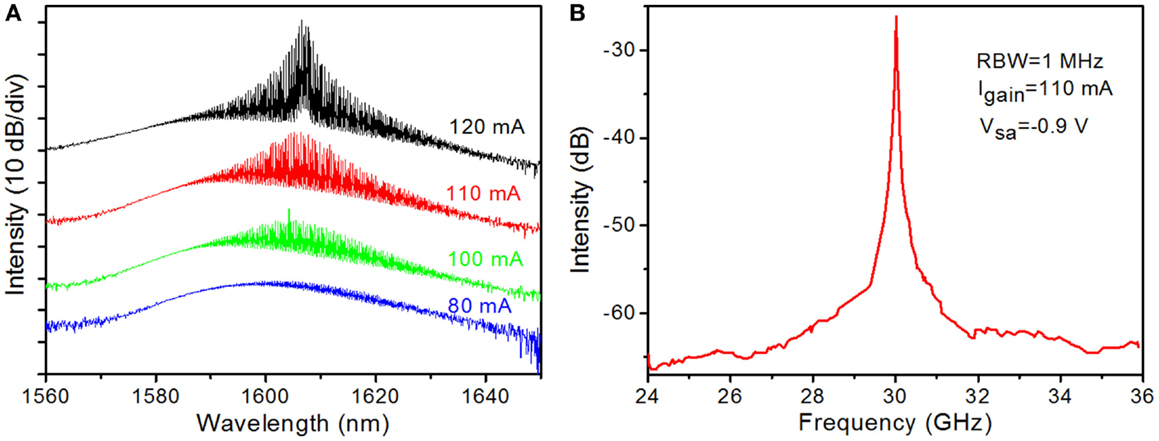
Figure 15. (A) The measured optical spectra of the III/V-on-silicon mode-locked laser at different injection currents to the gain section while the SA section is floating. (B) Measured RF spectrum of the III/V-on-Si MLL at 110 mA injection current and saturation voltage of −0.9 V. The RBW during measurement is 1 MHz.
Passive mode locking of the device is obtained by forward biasing the gain section (Igain) and reverse biasing (Vsa) or un-biasing the SA section. The mode locking behavior of the device is characterized by measuring the radio frequency (RF) spectrum using the spectrum analyzer (Agilent E4448A). Figure 15B shows the measured RF spectrum of the III/V-on-Si MLL at the injection current to the gain section (Igain) of 110 mA and reverse biasing the SA section at −0.9 V. The resolution bandwidth (RBW) during measurement is 1 MHz. The repetition frequency is about 30.0 GHz with signal-to-noise ratio above 30 dB. By changing Igain, it can be tuned to more than 30 GHz, giving clear evidence of passively mode locking of light signal. The measured RF linewidth of the injection locked laser is about 7 MHz by Lorentzian fitting the RF spectrum.
Summary and Future Outlook
Key Achievements
In summary, we reviewed in this paper the recent demonstrations of optical light source in silicon for the application of H-OEIC, with major focus on hybrid silicon lasers through wafer bonding technology. Furthermore, we proposed a proprietary high-throughput multiple dies-to-wafer (D2W) bonding technology by temporarily bonding III/V dies to a handle silicon wafer through pick-and-place process for subsequent simultaneous batch processing. Such high-throughput multiple D2W bonding technology features the merits of high bonding yield with unlimited III/V dies and scalability to whatever-size silicon wafers, thus is the key enabling technique toward potential manufacturability of large-scale H-OEIC. As proof-of-concept demonstration, we showed the III/V dies to silicon wafer bonding with up to 104 dies. Repeatable demonstrations of 16-III/V dies bonding to pre-patterned 200 mm silicon wafers are performed for the fabrication of hybrid silicon lasers with various laser cavities, including FP lasers, LC-DFB laser with side wall grating, and MLL.
Challenges and Future Outlook
However, there are still many key issues need to be addressed before the hybrid silicon laser applied to optical interconnects system. Here, we will only discuss three of the most important issues, including:
(1) the thermal management;
(2) the integration with other silicon photonic devices with full wafer processing capability; and
(3) the new platform beyond silicon for high-performance advanced hybrid lasers.
Thermal management is one of the major obstacles for achieving high-performance hybrid silicon lasers for practical applications (Sysak et al., 2011). Due to the poor thermal conductivity of the SOI BOX layer as well as the inter oxide layer between bonding surface, such layers would prevent the efficient heat dissipation to the silicon substrate, thus resulting in the poor laser performances, such as lower laser power. One of the simple ways to increase the thermal dissipation efficiency is to design the contact electrodes with thick and large area metal, serving as the top surface heat sink. Another efficient way for thermal dissipation is to remove the BOX layer in some areas and refill it with high thermal conductive materials such as polycrystalline silicon or metals, serving as thermal shunt (Liang et al., 2012). However, although such approach has been demonstrated with enhanced thermal management and increased laser performance, it still requires further development in order to further improve the performance.
The integration of such hybrid laser with the existing silicon photonics building blocks is another key issue before it is applied for H-OEIC. For most of the demonstrated hybrid silicon lasers, the silicon waveguide is normally with more than 500 nm thickness in order to ensure the optical index matching with III/V material for efficient light coupling to silicon waveguide. Such thick waveguide design is actually not compatible with the mainstream silicon photonics, with most of the key building blocks are demonstrated in 220 nm silicon wafers (Xu et al., 2014). Thus, novel designs taking care of both of these design considerations are required. Recently, Dong et al. (2014a,b) demonstrated novel integration scheme with associated transition structure via epitaxial growth of silicon in a pre-defined trench. Such epitaxial-grown silicon mesa also serves as the bonding interface with III/V gain material. Thus, the rest of the device area leaves with 220 nm silicon for other existing silicon photonic devices. Such novel demonstration sets a path toward the integration of hybrid silicon laser with existing silicon photonics building blocks. However, for practical integration with high-speed modulator and photodetector, which involves even complicated integration process with multiple oxide etch-back and CMP, it is still very challenging on how to ensure the flatness and smoothness of the bonding surface. More sophisticated design and further demonstration with integration of such are highly demanded.
The third issue is associated with current new demonstration trend that utilizes extremely low-loss SiN or SiON waveguide as the passive waveguide layer (Bovington et al., 2014; Luo et al., 2014). As we know, for some advanced type of hybrid lasers, such as the MLLs, extremely low optical loss is required for achieving high performances. The state-of-the-art demonstration of the silicon waveguide is still with propagation loss of ~2 dB/cm, which is higher comparing that of SiN waveguide of 0.1 dB/m (Bauters et al., 2011). Thus, III/V-SiN platform for hybrid lasers is another interest research area, which can address the loss issue. The integration between SiN waveguide and other SOI-based devices is also CMOS-compatible and ready for further application (Huang et al., 2014).
Conflict of Interest Statement
The authors declare that the research was conducted in the absence of any commercial or financial relationships that could be construed as a potential conflict of interest.
Acknowledgments
This work was supported by A*STAR SERC Future Data Center Technologies Thematic Strategic Research Programme under Grant No. 112 280 4038, and A*STAR – MINDEF Science and Technology Joint Funding Programme under Grant No.122 331 0076.
References
Alduino, A., and Paniccia, M. (2007). Interconnects: wiring electronics with light. Nat. Photonics 1, 153–155. doi: 10.1038/nphoton.2007.17
Alexe, M., and Gösele, U. (2004). Wafer Bonding: Applications and Technology. Berlin: Springer-Verlag.
Bauters, J. F., Heck, M. J., John, D. D., Barton, J. S., Blumenthal, D. J., Bowers, J. E., et al. (2011). “Ultra-low-loss (< 0.1 dB/m) planar silica waveguide technology,” in Paper Presented at the IEEE Photonics Conference (Arlington, VA: Marriott Crystal Gateway).
Beausoleil, R. G., Kuekes, P. J., Snider, G. S., Wang, S.-Y., and Williams, R. S. (2008). Nanoelectronic and nanophotonic interconnect. Proc. IEEE 96, 230–247. doi:10.1109/JPROC.2007.911057
Ben Bakir, B., Descos, A., Olivier, N., Bordel, D., Grosse, P., Augendre, E., et al. (2011). Electrically driven hybrid Si/III-V Fabry-Pérot lasers based on adiabatic mode transformers. Opt. Express 19, 10317–10325. doi:10.1364/OE.19.010317
Pubmed Abstract | Pubmed Full Text | CrossRef Full Text | Google Scholar
Bogaerts, W., Baets, R., Dumon, P., Wiaux, V., Beckx, S., Taillaert, D., et al. (2005). Nanophotonic waveguides in silicon-on-insulator fabricated with CMOS technology. J. Lightwave Technol. 23, 401–412. doi:10.1109/JLT.2004.834471
Bovington, J., Heck, M., and Bowers, J. (2014). Heterogeneous lasers and coupling to Si 3 N 4 near 1060 nm. Opt. Lett. 39, 6017–6020. doi:10.1364/OL.39.006017
Pubmed Abstract | Pubmed Full Text | CrossRef Full Text | Google Scholar
Boyraz, O., and Jalali, B. (2004). Demonstration of a silicon Raman laser. Opt. Express 12, 5269–5273. doi:10.1364/OPEX.12.005269
Pubmed Abstract | Pubmed Full Text | CrossRef Full Text | Google Scholar
Boyraz, O., and Jalali, B. (2005). Demonstration of directly modulated silicon Raman laser. Opt. Express 13, 796–800. doi:10.1364/OPEX.13.000796
Pubmed Abstract | Pubmed Full Text | CrossRef Full Text | Google Scholar
Camacho-Aguilera, R. E., Cai, Y., Patel, N., Bessette, J. T., Romagnoli, M., Kimerling, L. C., et al. (2012). An electrically pumped germanium laser. Opt. Express 20, 11316–11320. doi:10.1364/OE.20.011316
Pubmed Abstract | Pubmed Full Text | CrossRef Full Text | Google Scholar
Cheng, S.-L., Lu, J., Shambat, G., Yu, H.-Y., Saraswat, K., Vuckovic, J., et al. (2009). Room temperature 1.6 μm electroluminescence from Ge light emitting diode on Si substrate. Opt. Express 17, 10019–10024. doi:10.1364/OE.17.010019
Pubmed Abstract | Pubmed Full Text | CrossRef Full Text | Google Scholar
Christiansen, S. H., Singh, R., and Gosele, U. (2006). Wafer direct bonding: from advanced substrate engineering to future applications in micro/nanoelectronics. Proc. IEEE 94, 2060–2106. doi:10.1109/JPROC.2006.886026
Chu, T., Fujioka, N., and Ishizaka, M. (2009). Compact, lower-power-consumption wavelength tunable laser fabricated with silicon photonic-wire waveguide micro-ring resonators. Opt. Express 17, 14063–14068. doi:10.1364/OE.17.014063
Pubmed Abstract | Pubmed Full Text | CrossRef Full Text | Google Scholar
Creazzo, T., Marchena, E., Krasulick, S. B., Yu, P. K., Van Orden, D., Spann, J. Y., et al. (2013). Integrated tunable CMOS laser. Opt. Express 21, 28048–28053. doi:10.1364/OE.21.028048
Pubmed Abstract | Pubmed Full Text | CrossRef Full Text | Google Scholar
Dong, P., Hu, T.-C., Liow, T.-Y., Chen, Y.-K., Xie, C., Luo, X., et al. (2014a). Novel integration technique for silicon/III-V hybrid laser. Opt. Express 22, 26854–26861. doi:10.1364/OE.22.026854
Pubmed Abstract | Pubmed Full Text | CrossRef Full Text | Google Scholar
Dong, P., Liu, X., Chandrasekhar, S., Buhl, L. L., Aroca, R., and Chen, Y.-K. (2014b). Monolithic silicon photonic integrated circuits for compact 100 Gb/s coherent optical receivers and transmitters. IEEE J. Sel. Top. Quantum Electron. 20, 1–8. doi:10.1109/JSTQE.2013.2295181
Dong, P., Hu, T.-C., Zhang, L., Dinu, M., Kopf, R., Tate, A., et al. (2013). 1.9 μm hybrid silicon/iii-v semiconductor laser. Electron. Lett. 49:664. doi:10.1049/el.2013.0674
Dong, P., Liao, S., Feng, D., Liang, H., Zheng, D., Shafiiha, R., et al. (2009). Low V pp, ultralow-energy, compact, high-speed silicon electro-optic modulator. Opt. Express 17, 22484–22490. doi:10.1364/OE.17.022484
Pubmed Abstract | Pubmed Full Text | CrossRef Full Text | Google Scholar
Dumon, P., Bogaerts, W., Wiaux, V., Wouters, J., Beckx, S., Van Campenhout, J., et al. (2004). Low-loss SOI photonic wires and ring resonators fabricated with deep UV lithography. IEEE Photonics Technol. Lett. 16, 1328–1330. doi:10.1109/LPT.2004.826025
Fang, A. W., Jones, R., Park, H., Cohen, O., Raday, O., Paniccia, M. J., et al. (2007a). Integrated AlGaInAs-silicon evanescent racetrack laser and photodetector. Opt. Express 15, 2315–2322. doi:10.1364/OE.15.002315
Pubmed Abstract | Pubmed Full Text | CrossRef Full Text | Google Scholar
Fang, A. W., Park, H., Kuo, Y.-H., Jones, R., Cohen, O., Liang, D., et al. (2007b). Hybrid silicon evanescent devices. Mater. Today 10, 28–35. doi:10.1016/S1369-7021(07)70177-3
Fang, A. W., Koch, B. R., Gan, K.-G., Park, H., Jones, R., Cohen, O., et al. (2008a). A racetrack mode-locked silicon evanescent laser. Opt. Express 16, 1393–1398. doi:10.1364/OE.16.001393
Pubmed Abstract | Pubmed Full Text | CrossRef Full Text | Google Scholar
Fang, A. W., Koch, B. R., Jones, R., Lively, E., Liang, D., Kuo, Y.-H., et al. (2008b). A distributed Bragg reflector silicon evanescent laser. IEEE Photonics Technol. Lett 20, 1667–1669. doi:10.1109/LPT.2008.2003382
Fang, A. W., Lively, E., Kuo, Y.-H., Liang, D., and Bowers, J. E. (2008c). A distributed feedback silicon evanescent laser. Opt. Express 16, 4413–4419. doi:10.1364/OE.16.001393
Pubmed Abstract | Pubmed Full Text | CrossRef Full Text | Google Scholar
Fang, A. W., Park, H., Cohen, O., Jones, R., Paniccia, M. J., and Bowers, J. E. (2006). Electrically pumped hybrid AlGaInAs-silicon evanescent laser. Opt. Express 14, 9203–9210. doi:10.1364/OE.14.009203
Pubmed Abstract | Pubmed Full Text | CrossRef Full Text | Google Scholar
Fang, A. W., Sysak, M. N., Koch, B. R., Jones, R., Lively, E., Kuo, Y.-H., et al. (2009). Single-wavelength silicon evanescent lasers. IEEE J. Sel. Top. Quantum Electron. 15, 535. doi:10.1364/OE.22.005448
Pubmed Abstract | Pubmed Full Text | CrossRef Full Text | Google Scholar
Fang, Q., Song, J., Luo, X., Jia, L., Yu, M., Lo, G., et al. (2012). High efficiency ring-resonator filter with NiSi heater. IEEE Photonics Technol. Lett. 24, 350–352. doi:10.1109/LPT.2011.2177816
Fedeli, J., Di Cioccio, L., Marris-Morini, D., Vivien, L., Orobtchouk, R., Rojo-Romeo, P., et al. (2008). Development of silicon photonics devices using microelectronic tools for the integration on top of a CMOS wafer. Adv. Opt. Tech. 2008. doi:10.1155/2008/412518
Feng, S., Lei, T., Chen, H., Cai, H., Luo, X., and Poon, A. W. (2012). Silicon photonics: from a microresonator perspective. Laser Photonics Rev. 6, 145–177. doi:10.1002/lpor.201100020
Fujioka, N., Chu, T., and Ishizaka, M. (2010). Compact and low power consumption hybrid integrated wavelength tunable laser module using silicon waveguide resonators. J. Lightwave Technol. 28, 3115–3120. doi:10.1109/JLT.2010.2073445
Goodman, J. W., Leonberger, F. J., Kung, S.-Y., and Athale, R. A. (1984). Optical interconnections for VLSI systems. Proc. IEEE 72, 850–866. doi:10.1109/PROC.1984.12943
Grenouillet, L., Dupont, T., Philippe, P., Harduin, J., Olivier, N., Bordel, D., et al. (2012). Hybrid integration for silicon photonics applications. Opt. Quant. Electron. 44, 527–534. doi:10.1038/nnano.2014.215
Pubmed Abstract | Pubmed Full Text | CrossRef Full Text | Google Scholar
Guha, B., Kyotoku, B. B., and Lipson, M. (2010). CMOS-compatible athermal silicon microring resonators. Opt. Express 18, 3487–3493. doi:10.1364/OE.18.003487
Pubmed Abstract | Pubmed Full Text | CrossRef Full Text | Google Scholar
Guillot, G., and Pavesi, L. (2006). Optical Interconnects: The Silicon Approach. Berlin: Springer-Verlag.
Han, H.-S., Seo, S.-Y., and Shin, J. H. (2001). Optical gain at 1.54 μm in erbium-doped silicon nanocluster sensitized waveguide. Appl. Phys. Lett. 79, 4568–4570. doi:10.1063/1.1419035
Hattori, H. T., Seassal, C., Touraille, E., Rojo-Romeo, P., Letartre, X., Hollinger, G., et al. (2006). Heterogeneous integration of microdisk lasers on silicon strip waveguides for optical interconnects. IEEE Photonics Technol. Lett. 18, 223–225. doi:10.1109/LPT.2005.861542
Hong, T., Ran, G.-Z., Chen, T., Pan, J.-Q., Chen, W.-X., Wang, Y., et al. (2010). A selective-area metal bonding InGaAsP–Si laser. IEEE Photonics Technol. Lett. 22, 1141–1143. doi:10.1364/OE.22.005448
Pubmed Abstract | Pubmed Full Text | CrossRef Full Text | Google Scholar
Huang, Y., Song, J., Luo, X., Liow, T.-Y., and Lo, G.-Q. (2014). CMOS compatible monolithic multi-layer Si3N4-on-SOI platform for low-loss high performance silicon photonics dense integration. Opt. Express 22, 21859–21865. doi:10.1364/OE.22.021859
Pubmed Abstract | Pubmed Full Text | CrossRef Full Text | Google Scholar
Jalali, B., and Fathpour, S. (2006). Silicon photonics. J. Lightwave Technol. 24, 4600–4615. doi:10.1109/JLT.2006.885782
Justice, J., Bower, C., Meitl, M., Mooney, M. B., Gubbins, M. A., and Corbett, B. (2012). Wafer-scale integration of group III-V lasers on silicon using transfer printing of epitaxial layers. Nat. Photonics 6, 610–614. doi:10.1038/nphoton.2012.204
Keyvaninia, S., Muneeb, M., Stanković, S., Roelkens, G., Van Thourhout, D., and Fedeli, J. (2012). “Multiple die-to-wafer adhesive bonding for heterogeneous integration,” in Paper Presented at the 16th European Conference on Integrated Optics (ECIO-2012). Sitges, Barcelona, Spain.
Keyvaninia, S., Roelkens, G., Van Thourhout, D., Jany, C., Lamponi, M., Le Liepvre, A., et al. (2013a). Demonstration of a heterogeneously integrated III-V/SOI single wavelength tunable laser. Opt. Express 21, 3784–3792. doi:10.1364/OE.21.003784
Pubmed Abstract | Pubmed Full Text | CrossRef Full Text | Google Scholar
Keyvaninia, S., Verstuyft, S., Pathak, S., Lelarge, F., Duan, G.-H., Bordel, D., et al. (2013b). III-V-on-silicon multi-frequency lasers. Opt. Express 21, 13675–13683. doi:10.1364/OE.21.013675
Pubmed Abstract | Pubmed Full Text | CrossRef Full Text | Google Scholar
Keyvaninia, S., Verstuyft, S., Van Landschoot, L., Lelarge, F., Duan, G.-H., Messaoudene, S., et al. (2013c). Heterogeneously integrated III-V/silicon distributed feedback lasers. Opt. Lett. 38, 5434–5437. doi:10.1364/OL.38.005434
Pubmed Abstract | Pubmed Full Text | CrossRef Full Text | Google Scholar
Kissinger, G., and Kissinger, W. (1993). Void-free silicon-wafer-bond strengthening in the 200–400 C range. Sens. Actuators A 36, 149–156. doi:10.1016/0924-4247(93)85009-5
Kostrzewa, M., Di Cioccio, L., Zussy, M., Roussin, J., Fedeli, J., Kernevez, N., et al. (2006). InP dies transferred onto silicon substrate for optical interconnects application. Sens. Actuators A 125, 411–414. doi:10.1016/j.sna.2005.07.023
Kurczveil, G., Heck, M. J., Peters, J. D., Garcia, J. M., Spencer, D., and Bowers, J. E. (2011). An integrated hybrid silicon multiwavelength AWG laser. IEEE J. Sel. Top. Quantum Electron. 17, 1521–1527. doi:10.1109/JSTQE.2011.2112639
Lasky, J. (1986). Wafer bonding for silicon-on-insulator technologies. Appl. Phys. Lett. 48, 78–80. doi:10.1063/1.96768
Lee, A., Jiang, Q., Tang, M., Seeds, A., and Liu, H. (2012). Continuous-wave InAs/GaAs quantum-dot laser diodes monolithically grown on Si substrate with low threshold current densities. Opt. Express 20, 22181–22187. doi:10.1364/OE.20.022181
Pubmed Abstract | Pubmed Full Text | CrossRef Full Text | Google Scholar
Levaufre, G., Le Liepvre, A., Jany, C., Accard, A., Kaspar, P., Brenot, R., et al. (2014). “Hybrid III-V/silicon tunable laser directly modulated at 10Gbit/s for short reach/access networks,” in Paper Presented at the Optical Communication (ECOC), 2014 European Conference on, Cannes France.
Liang, D., and Bowers, J. (2008). Highly efficient vertical outgassing channels for low-temperature InP-to-silicon direct wafer bonding on the silicon-on-insulator substrate. J. Vac. Sci Technol. B 26, 1560–1568. doi:10.1116/1.2943667
Liang, D., Fang, A. W., Chen, H.-W., Sysak, M. N., Koch, B. R., Lively, E., et al. (2009a). Hybrid silicon evanescent approach to optical interconnects. Appl. Phys. A 95, 1045–1057. doi:10.1007/s00339-009-5118-1
Liang, D., Fiorentino, M., Okumura, T., Chang, H.-H., Spencer, D. T., Kuo, Y.-H., et al. (2009b). Electrically-pumped compact hybrid silicon microring lasers for optical interconnects. Opt. Express 17, 20355–20364. doi:10.1364/OE.17.020355
Pubmed Abstract | Pubmed Full Text | CrossRef Full Text | Google Scholar
Liang, D., Fiorentino, M., Srinivasan, S., Bowers, J. E., and Beausoleil, R. G. (2011). Low threshold electrically-pumped hybrid silicon microring lasers. IEEE J. Sel. Top. Quantum Electron. 17, 1528–1533. doi:10.1109/JSTQE.2010.2103552
Liang, D., Roelkens, G., Baets, R., and Bowers, J. E. (2010). Hybrid integrated platforms for silicon photonics. Materials 3, 1782–1802. doi:10.1038/nnano.2014.215
Pubmed Abstract | Pubmed Full Text | CrossRef Full Text | Google Scholar
Liang, D., Srinivasan, S., Fiorentino, M., Kurczveil, G., Bowers, J., and Beausoleil, R. (2012). “A metal thermal shunt design for hybrid silicon microring laser,” in Paper Presented at the Optical Interconnects Conference, 2012 (Santa Fe, NM: IEEE).
Lim, A. E.-J., Song, J., Fang, Q., Li, C., Tu, X., Duan, N., et al. (2014). Review of silicon photonics foundry efforts. IEEE J. Sel. Top. Quantum Electron. 20, 8300112. doi:10.1109/JSTQE.2013.2293274
Liow, T.-Y., Song, J., Tu, X., Lim, A.-J., Fang, Q., Duan, N., et al. (2013). Silicon optical interconnect device technologies for 40 Gb/s and beyond. IEEE J. Sel. Top. Quantum Electron. 19, 8200312–8200312. doi:10.1109/JSTQE.2012.2218580
Lipson, M. (2005). Guiding, modulating, and emitting light on silicon-challenges and opportunities. J. Lightwave Technol. 23, 4222. doi:10.1109/JLT.2005.858225
Liu, H., Wang, T., Jiang, Q., Hogg, R., Tutu, F., Pozzi, F., et al. (2011). Long-wavelength InAs/GaAs quantum-dot laser diode monolithically grown on Ge substrate. Nat. Photonics 5, 416–419. doi:10.1364/OE.20.022181
Pubmed Abstract | Pubmed Full Text | CrossRef Full Text | Google Scholar
Liu, J., Sun, X., Camacho-Aguilera, R., Kimerling, L. C., and Michel, J. (2010). Ge-on-Si laser operating at room temperature. Opt. Lett. 35, 679–681. doi:10.1364/OL.35.000679
Pubmed Abstract | Pubmed Full Text | CrossRef Full Text | Google Scholar
Liu, J., Sun, X., Kimerling, L. C., and Michel, J. (2009). Direct-gap optical gain of Ge on Si at room temperature. Opt. Lett. 34, 1738–1740. doi:10.1364/OL.34.001738
Pubmed Abstract | Pubmed Full Text | CrossRef Full Text | Google Scholar
Liu, J., Sun, X., Pan, D., Wang, X., Kimerling, L. C., Koch, T. L., et al. (2007). Tensile-strained, n-type Ge as a gain medium for monolithic laser integration on Si. Opt. Express 15, 11272–11277. doi:10.1364/OE.15.011272
Pubmed Abstract | Pubmed Full Text | CrossRef Full Text | Google Scholar
Luo, X., Song, J., Feng, S., Poon, A. W., Liow, T.-Y., Yu, M., et al. (2012). Silicon high-order coupled-microring-based electro-optical switches for on-chip optical interconnects. IEEE Photonics Technol. Lett. 24, 821–823. doi:10.1109/LPT.2012.2188829
Luo, X., Song, J., Zhou, H., Liow, T. Y., Yu, M., and Lo, P. G. Q. (2014). United States Patent No. US 2014/0153600 A1.
Maszara, W. (1991). Silicon-on-insulator by wafer bonding: a review. J. Electrochem. Soc. 138, 341–347. doi:10.1149/1.2085575
Mechet, P., Verstuyft, S., De Vries, T., Spuesens, T., Regreny, P., Van Thourhout, D., et al. (2013). Unidirectional III-V microdisk lasers heterogeneously integrated on SOI. Opt. Express 21, 19339–19352. doi:10.1364/OE.21.019339
Pubmed Abstract | Pubmed Full Text | CrossRef Full Text | Google Scholar
Michel, J., Liu, J., and Kimerling, L. C. (2010). High-performance Ge-on-Si photodetectors. Nat. Photonics 4, 527–534. doi:10.1038/nphoton.2010.157
Miller, D. A. (2000). Optical interconnects to silicon. IEEE J. Sel. Top. Quantum Electron. 6, 1312–1317. doi:10.1109/2944.902184
Miller, D. A. (2009). Device requirements for optical interconnects to silicon chips. Proc. IEEE 97, 1166–1185. doi:10.1109/JPROC.2009.2014298
Ohashi, K., Nishi, K., Shimizu, T., Nakada, M., Fujikata, J., Ushida, J., et al. (2009). On-chip optical interconnect. Proc. IEEE 97, 1186–1198. doi:10.1109/JPROC.2009.2020331
Park, H., Fang, A., Kodama, S., and Bowers, J. (2005). Hybrid silicon evanescent laser fabricated with a silicon waveguide and III-V offset quantum wells. Opt. Express 13, 9460–9464. doi:10.1364/OPEX.13.009460
Pubmed Abstract | Pubmed Full Text | CrossRef Full Text | Google Scholar
Pasquariello, D., and Hjort, K. (2002). Plasma-assisted InP-to-Si low temperature wafer bonding. IEEE J. Sel. Top. Quantum Electron. 8, 118–131. doi:10.1109/2944.991407
Pubmed Abstract | Pubmed Full Text | CrossRef Full Text | Google Scholar
Pavesi, L., Dal Negro, L., Mazzoleni, C., Franzo, G., and Priolo, F. (2000). Optical gain in silicon nanocrystals. Nature 408, 440–444. doi:10.1038/35044012
Poon, A. W., Luo, X., Xu, F., and Chen, H. (2009a). Cascaded microresonator-based matrix switch for silicon on-chip optical interconnection. Proc. IEEE 97, 1216–1238. doi:10.1109/JPROC.2009.2014884
Poon, A. W., Luo, X., Zhou, L., Li, C., Lee, J. Y., Xu, F., et al. (2009b). “Microresonator-based devices on a silicon chip: novel shaped cavities and resonance coherent interference,” in Practical Applications of Microresonators in Optics and Photonics, ed. A. B. Matsko (Boca Raton, FL: CRC Press), 211–263.
Reed, G. T., and Knights, A. P. (2004). Silicon Photonics: An Introduction. England: John Wiley & Sons.
Reed, G. T., Mashanovich, G., Gardes, F., and Thomson, D. (2010). Silicon optical modulators. Nat. Photonics 4, 518–526. doi:10.1038/nphoton.2010.219
Roelkens, G., Van Thourhout, D., and Baets, R. (2005). Ultra-thin benzocyclobutene bonding of III–V dies onto SOI substrate. Electron. Lett. 41, 561–562. doi:10.1049/el:20050807
Roelkens, G., Van Thourhout, D., Baets, R., and Smit, M. (2006). Laser emission and photodetection in an InP/InGaAsP layer integrated on and coupled to a Silicon-on-Insulator waveguide circuit. Opt. Express 14, 8154–8159. doi:10.1364/OE.14.008154
Pubmed Abstract | Pubmed Full Text | CrossRef Full Text | Google Scholar
Rong, H., Jones, R., Liu, A., Cohen, O., Hak, D., Fang, A., et al. (2005a). A continuous-wave Raman silicon laser. Nature 433, 725–728. doi:10.1038/nature03273
Rong, H., Liu, A., Jones, R., Cohen, O., Hak, D., Nicolaescu, R., et al. (2005b). An all-silicon Raman laser. Nature 433, 292–294. doi:10.1038/nature03273
Rong, H., Xu, S., Kuo, Y.-H., Sih, V., Cohen, O., Raday, O., et al. (2007). Low-threshold continuous-wave Raman silicon laser. Nat. Photonics 1, 232–237. doi:10.1038/nphoton.2007.29
Rotem, E., Shainline, J. M., and Xu, J. M. (2007a). Electroluminescence of nanopatterned silicon with carbon implantation and solid phase epitaxial regrowth. Opt. Express 15, 14099–14106. doi:10.1364/OE.15.014099
Pubmed Abstract | Pubmed Full Text | CrossRef Full Text | Google Scholar
Rotem, E., Shainline, J. M., and Xu, J. M. (2007b). Enhanced photoluminescence from nanopatterned carbon-rich silicon grown by solid-phase epitaxy. Appl. Phys. Lett. 91, 051127. doi:10.1063/1.2766843
Seassal, C., Rojo-Romeo, P., Letartre, X., Viktorovitch, P., Hollinger, G., Jalaguier, E., et al. (2001). InP microdisk lasers on silicon wafer: CW room temperature operation at 1.6 μm. Electron. Lett. 37, 222–223. doi:10.1049/el:20010173
Shainline, J. M., and Xu, J. (2007). Silicon as an emissive optical medium. Laser Photonics Rev. 1, 334–348. doi:10.1002/lpor.200710021
Song, J., Luo, X., Tu, X., Jia, L., Fang, Q., Liow, T.-Y., et al. (2013). On-chip quasi-digital optical switch using silicon microring resonator-coupled Mach-Zehnder interferometer. Opt. Express 21, 12767–12775. doi:10.1364/OE.21.012767
Pubmed Abstract | Pubmed Full Text | CrossRef Full Text | Google Scholar
Soref, R. (2006). The past, present, and future of silicon photonics. IEEE J. Sel. Top. Quantum Electron. 12, 1678–1687. doi:10.1021/ar900141y
Pubmed Abstract | Pubmed Full Text | CrossRef Full Text | Google Scholar
Soref, R., and Lorenzo, J. (1985). Single-crystal silicon: a new material for 1.3 and 1.6 μm integrated-optical components. Electron. Lett. 21, 953–954. doi:10.1049/el:19850673
Sparacin, D. K., Spector, S. J., and Kimerling, L. C. (2005). Silicon waveguide sidewall smoothing by wet chemical oxidation. J. Lightwave Technol. 23, 2455. doi:10.1109/JLT.2005.851328
Stanković, S., Jones, R., Sysak, M. N., Heck, J. M., Roelkens, G., and Van Thourhout, D. (2011). 1310-nm hybrid III–V/Si Fabry–Pérot laser based on adhesive bonding. IEEE Photonics Technol. Lett. 23, 1781–1783. doi:10.1109/LPT.2011.2169397
Stanković, S., Jones, R., Sysak, M. N., Heck, J. M., Roelkens, G., and Van Thourhout, D. (2012). Hybrid III–V/Si distributed-feedback laser based on adhesive bonding. IEEE Photonics Technol. Lett. 24, 2155–2158. doi:10.1109/LPT.2012.2223666
Stanković, S., Van Thourhout, D., Roelkens, G., Jones, R., Heck, J., and Sysak, M. (2010). Die-to-die adhesive bonding for evanescently-coupled photonic devices. ECS Trans. 33, 411–420. doi:10.1149/1.3483531
Sun, X., Liu, H.-C., and Yariv, A. (2009a). Adiabaticity criterion and the shortest adiabatic mode transformer in a coupled-waveguide system. Opt. Lett. 34, 280–282. doi:10.1364/OL.34.000280
Pubmed Abstract | Pubmed Full Text | CrossRef Full Text | Google Scholar
Sun, X., Liu, J., Kimerling, L. C., and Michel, J. (2009b). Direct gap photoluminescence of n-type tensile-strained Ge-on-Si. Appl. Phys. Lett. 95, 011911–011911–011913. doi:10.1364/OL.38.000652
Pubmed Abstract | Pubmed Full Text | CrossRef Full Text | Google Scholar
Sun, X., Liu, J., Kimerling, L. C., and Michel, J. (2009c). Room-temperature direct bandgap electroluminesence from Ge-on-Si light-emitting diodes. Opt. Lett. 34, 1198–1200. doi:10.1364/OL.34.001198
Pubmed Abstract | Pubmed Full Text | CrossRef Full Text | Google Scholar
Sysak, M. N., Liang, D., Jones, R., Kurczveil, G., Piels, M., Fiorentino, M., et al. (2011). Hybrid silicon laser technology: a thermal perspective. IEEE J. Sel. Top. Quantum Electron. 17, 1490–1498. doi:10.1109/JSTQE.2011.2109940
Tanabe, K., Guimard, D., Bordel, D., Iwamoto, S., and Arakawa, Y. (2010). Electrically pumped 1.3 μm room-temperature InAs/GaAs quantum dot lasers on Si substrates by metal-mediated wafer bonding and layer transfer. Opt. Express 18, 10604–10608. doi:10.1364/OE.18.010604
Pubmed Abstract | Pubmed Full Text | CrossRef Full Text | Google Scholar
Tatsumi, T., Tanabe, K., Watanabe, K., Iwamoto, S., and Arakawa, Y. (2012). 1.3 μm InAs/GaAs quantum dot lasers on Si substrates by low-resistivity, Au-free metal-mediated wafer bonding. J. Appl. Phys. 112, 033107. doi:10.1063/1.4742198
Tong, Q.-Y., and Goesele, U. (1999). Semiconductor Wafer Bonding: Science and Technology. Wiley, 1998.
Tu, X., Chang, K.-F., Liow, T.-Y., Song, J., Luo, X., Jia, L., et al. (2014). Silicon optical modulator with shield coplanar waveguide electrodes. Opt. Express 22, 23724–23731. doi:10.1364/OE.22.023724
Pubmed Abstract | Pubmed Full Text | CrossRef Full Text | Google Scholar
Tu, X., Liow, T.-Y., Song, J., Luo, X., Fang, Q., Yu, M., et al. (2013). 50-Gb/s silicon optical modulator with traveling-wave electrodes. Opt. Express 21, 12776–12782. doi:10.1364/OE.21.012776
Pubmed Abstract | Pubmed Full Text | CrossRef Full Text | Google Scholar
Urino, Y., Shimizu, T., Okano, M., Hatori, N., Ishizaka, M., Yamamoto, T., et al. (2011). First demonstration of high density optical interconnects integrated with lasers, optical modulators, and photodetectors on single silicon substrate. Opt. Express 19, B159–B165. doi:10.1364/OE.19.00B159
Pubmed Abstract | Pubmed Full Text | CrossRef Full Text | Google Scholar
Van Campenhout, J., Green, W. M., Assefa, S., and Vlasov, Y. A. (2009). Low-power, 2x2 silicon electro-optic switch with 110-nm bandwidth for broadband reconfigurable optical networks. Opt. Express 17, 24020–24029. doi:10.1364/OE.17.024020
Pubmed Abstract | Pubmed Full Text | CrossRef Full Text | Google Scholar
Van Campenhout, J., Liu, L., Romeo, P. R., Van Thourhout, D., Seassal, C., Regreny, P., et al. (2008). A compact SOI-integrated multiwavelength laser source based on cascaded InP microdisks. IEEE Photonics Technol. Lett. 20, 1345–1347. doi:10.1109/LPT.2008.926857
Van Campenhout, J., Rojo Romeo, P., Regreny, P., Seassal, C., Van Thourhout, D., Verstuyft, S., et al. (2007). Electrically pumped InP-based microdisk lasers integrated with a nanophotonic silicon-on-insulator waveguide circuit. Opt. Express 15, 6744–6749. doi:10.1364/OE.15.006744
Pubmed Abstract | Pubmed Full Text | CrossRef Full Text | Google Scholar
Xia, F., Sekaric, L., and Vlasov, Y. (2006). Ultracompact optical buffers on a silicon chip. Nat. Photonics 1, 65–71. doi:10.1038/nphoton.2006.42
Xiao, S., Khan, M. H., Shen, H., and Qi, M. (2007). Multiple-channel silicon micro-resonator based filters for WDM applications. Opt. Express 15, 7489–7498. doi:10.1364/OE.15.009386
Xu, D.-X., Schmid, J. H., Reed, G. T., Mashanovich, G. Z., Thomson, D. J., Nedeljkovic, M., et al. (2014). Silicon photonic integration platform-have we found the sweet spot? IEEE J. Sel. Top. Quantum Electron. 20, 189–205. doi:10.1109/JSTQE.2014.2299634
Yang, H., Zhao, D., Chuwongin, S., Seo, J.-H., Yang, W., Shuai, Y., et al. (2012). Transfer-printed stacked nanomembrane lasers on silicon. Nat. Photonics 6, 615–620. doi:10.1038/nphoton.2012.160
Yariv, A., and Sun, X. (2007). Supermode Si/III-V hybrid lasers, optical amplifiers and modulators: a proposal and analysis. Opt. Express 15, 9147–9151. doi:10.1364/OE.15.009147
Pubmed Abstract | Pubmed Full Text | CrossRef Full Text | Google Scholar
Zhang, C., Srinivasan, S., Tang, Y., Heck, M. J., Davenport, M. L., and Bowers, J. E. (2014). Low threshold and high speed short cavity distributed feedback hybrid silicon lasers. Opt. Express 22, 10202–10209. doi:10.1364/OE.22.010202
Pubmed Abstract | Pubmed Full Text | CrossRef Full Text | Google Scholar
Zhou, L., and Poon, A. W. (2007). Electrically reconfigurable silicon microring resonator-based filter with waveguide-coupled feedback. Opt. Express 15, 9194–9204. doi:10.1364/OE.15.009194
Pubmed Abstract | Pubmed Full Text | CrossRef Full Text | Google Scholar
Keywords: silicon photonics, hybrid lasers, heterogeneous integration, die-to-wafer bonding, optoelectronic integrated circuits
Citation: Luo X, Cao Y, Song J, Hu X, Cheng Y, Li C, Liu C, Liow T-Y, Yu M, Wang H, Wang QJ and Lo PG-Q (2015) High-throughput multiple dies-to-wafer bonding technology and III/V-on-Si hybrid lasers for heterogeneous integration of optoelectronic integrated circuits. Front. Mater. 2:28. doi: 10.3389/fmats.2015.00028
Received: 08 January 2015; Paper pending published: 13 February 2015;
Accepted: 17 March 2015; Published online: 07 April 2015.
Edited by:
Laurent Vivien, Université Paris-Sud, FranceReviewed by:
Junichi Fujikata, Photonics Electronics Technology Research Association, JapanYasuhiko Ishikawa, The University of Tokyo, Japan
Copyright: © 2015 Luo, Cao, Song, Hu, Cheng, Li, Liu, Liow, Yu, Wang, Wang and Lo. This is an open-access article distributed under the terms of the Creative Commons Attribution License (CC BY). The use, distribution or reproduction in other forums is permitted, provided the original author(s) or licensor are credited and that the original publication in this journal is cited, in accordance with accepted academic practice. No use, distribution or reproduction is permitted which does not comply with these terms.
*Correspondence: Patrick Guo-Qiang Lo, Institute of Microelectronics, Agency for Science, Technology and Research (A*STAR), Singapore Science Park II, 11 Science Park Road, 117685 Singapore e-mail: logq@ime.a-star.edu.sg