Group IV direct band gap photonics: methods, challenges, and opportunities
 Richard Geiger
 Thomas Zabel
 Hans Sigg
- Laboratory for Micro- and Nanotechnology, Paul Scherrer Institut, Villigen, Switzerland
The concept of direct band gap group IV materials may offer a paradigm change for Si-photonics concerning the monolithic implementation of light emitters: the idea is to integrate fully compatible group IV materials with equally favorable optical properties as the chemically incompatible group III–V-based systems. The concept involves either mechanically applied strain on Ge or alloying of Ge with Sn, which permits to drastically improve the radiative efficiency of Ge. The favorable optical properties result from a modified band structure transformed from an indirect to a direct one. The first demonstration of such a direct band gap laser has recently been accomplished in GeSn. This demonstration proves the capability of this new concept, which may permit a qualitative as well as a quantitative expansion of Si-photonics in not only traditional but also new areas of applications. This review aims to discuss the challenges along this path in terms of fabrication, characterization, and fundamental understanding, and will elaborate on evoking opportunities of this new class of group IV-based laser materials.
Introduction
The Si-based optical platform is rapidly changing the landscape of photonics by offering powerful solutions, for example, for data links (Miller, 2010) and sensing (Passaro et al., 2012) to name only two out of many. This development has taken place in spite of the fact that Si itself is a poor emitter of light. This is without a doubt due to the fact that Si technology as used in very large-scale integration (VLSI) and complementary metal-oxide-semiconductor (CMOS) technology is extremely mature and advanced. This fact seemingly compensates for the shortfalls in concepts for Si to generate light.
Nowadays, group III–V materials are implemented to integrate active light sources onto the Si platform by using involved coupling schemes and/or heterogeneous integration (Fang et al., 2013). However, because these materials are chemically intolerant to Si, their integration bears a lot of burdens, which raises the fabrication costs. Strongly preferred are materials that are compatible to Si, tolerated by the technology (preferentially CMOS), and capable of producing light similar in efficiency to traditional group III–V semiconductor systems.
In direct band gap systems, light generation is based on radiative recombination of electrons and holes, both with practically the same momentum as schematically shown in Figure 1A. In unstrained, i.e., “regular” bulk Ge, however, the excited electrons will preferentially occupy the lower conduction band energy states of the L-valley. In Ge, the momentum of the electrons does, thus, not match those of the holes, which occupy the degenerated heavy- and light-mass valence bands at the Γ-point (c.f. Figure 1B). The appearing momentum mismatch requires a phonon for the recombination. But note that except the position of the indirect L-valley, which is in Ge 140 meV below the Γ valley minimum, the band alignments near the Γ-point in system A (say InGaAs, one of the most prominent group III–V systems used for lasing) and B are very similar. To achieve the favorable direct recombination condition also for Ge, we need to find a way to inject electrons into that conduction band valley with its energetic minimum at the Γ-point. This is realized in the most straightforward fashion when all unwanted electron levels are energetically shifted above the Γ-states, which is equivalent to transfer the system from a fundamentally indirect to a fundamentally direct one.
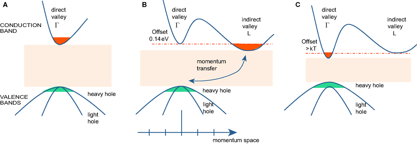
Figure 1. Band structure in momentum space (A) direct band gap semiconductor. Electron/hole recombination occurs at the Γ-point. (B) Unstrained Ge. Electrons occupy the conduction band states of the L-valleys. Radiative recombination is hindered by the momentum mismatch. (C) Due to strain (or alloying with Sn), the band gap of Ge (GeSn) shrinks and the population of electrons at the Γ-point increases.
We will discuss the two methods that make this conversion possible. One involves the application of tensile strain, while the second approach relies on alloying Ge with Sn. Thus, the obtained band alignments are depicted in Figure 1C. With either one of the methods, the Γ-valley can be reduced below the indirect one at L enabling efficient carrier injection into the Γ-valley. Moreover, the VB degeneracy is lifted depending on the strain state and its loading, biaxial or uniaxial, c.f. Section “Modeling” for more details.
In Figure 2, we show the state-of-the-art of the strain and alloying approach toward the realization of a direct band gap group IV material. For our discussion, we selected those approaches that are potentially compatible with CMOS fabrication and are suited for optical applications. Very thin membranes (Sánchez-Pérez et al., 2011), nanowires clamped in bulky mechanical strain apparatus (Greil et al., 2012), Ge bulk layers on III–V substrates (Huo et al., 2011), etc., are not considered here because they are unpractical for integration on Si. Not considered either is light emission from Si-based quantum wells and defects; for a recent review, see Saito et al. (2014). In our compilation, Figure 2, we benchmark the two strain loadings (uniaxial and biaxial) and Sn alloy composition against the achieved relative band offset, ΔE/E0, where an offset ΔE of 100% is equal to E0 ~ 140 meV for the case of unstrained Ge. An offset parameter of 0 meV (0%) corresponds, thus, to Γ- and L-valleys having their band edges at the same energy.
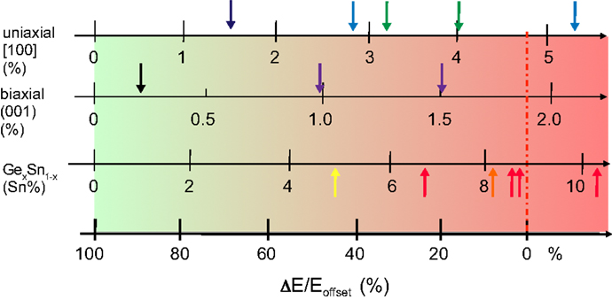
Figure 2. Relative offset of the Γ- and L-conduction band minima realized in Ge either by uniaxial tensile strain along [100] direction [dark blue: (Capellini et al., 2013), light blue: (Nam et al., 2013; Sukhdeo et al., 2014), olive: (Süess et al., 2013; Geiger et al., 2014c)], biaxial tensile strain on (001) oriented substrate [black: (Liu et al., 2010); violet: (Ghrib et al., 2013, 2015)] or by alloying with Sn [yellow: (Chen et al., 2013a); orange (Gupta et al., 2013b); red: (Wirths et al., 2015)]. The shown offset versus Sn concentration relates to the unstrained case. About 100% (0%) offset refers to 140 meV (vanishing energy offset). Hence, the dash-dotted line marks the transition from an indirect to a direct band gap semiconductor.
The black arrow on the left hand side of the second line in Figure 2 marks the case of highly n-doped Ge (Liu et al., 2010), where a maximum of 0.25% biaxial strain is accomplished. This value of 0.25% is the one typically obtained from direct epitaxy of Ge on Si. It arises due to the difference between the thermal expansion coefficients of Si and Ge (Michel et al., 2010). High n-doping is introduced to fill the parasitic indirect states (Xiaochen et al., 2010). Such doping does not transform the material into a direct gap system, but it appeared that under optical excitation and electrical pumping the light emission shows an intensity threshold as well as linewidth narrowing (Liu et al., 2010; Camacho-Aguilera et al., 2012). These results became widely known as the optically and electrically pumped Ge-laser. However, since the time when these announcements were made in 2010 and 2012, only one other demonstration of these effects has been reported so far (Koerner et al., 2015). This very recent and only result concerns a Ge diode structure with an unstrained active region doped at 3 × 1019 cm−3. The obtained emission spectra are similar to the one from the original work from the MIT group. However, as we will show below, these spectra significantly differ in several aspects – the intensity, the linewidth, and the Fabry–Perot (FP) multi-mode behavior – from those obtained with the here discussed direct band gap lasers. Moreover, as will be discussed in Section “Lifetime, Gain, and Loss,” these Ge-lasing observations are contradicted by gain experiments (Carroll et al., 2012) as well as by theoretical analysis performed by several groups (Liu et al., 2007; Chow, 2012; Dutt et al., 2012; Peschka et al., 2015) when the lasing current density threshold is calculated using realistic non-radiative lifetimes (Geiger et al., 2014a). As the experimental foundation for understanding this peculiar threshold behavior of low strained (and in one case even unstrained) Ge is ambiguous, we will focus here on reports concerning direct band gap group IV systems, which includes the first unmistakable proof of interband lasing in a group IV system. Without doubt, with the advent of direct band gap systems showing unambiguous lasing, an excellent opportunity is created, which will help to unravel in the very near future above raised questions regarding the lasing in highly n-doped Ge.
Coming back to Figure 2: the arrows colored in violet depict 1.0 and 1.5% biaxially tensilely strained structures that have been achieved via deposition of Si–Nitride (SiN) stressor layers (Ghrib et al., 2013, 2015). This strain is equivalent to a band offset of ~70 and 30 meV, which corresponds to 50 and 30% of the unstrained band offset value, respectively. So far, the highest strain values are obtained in suspended microbridges under uniaxial loading as is shown on the top stroke. There, the ~0.25% biaxial prestrain is enhanced and transformed into uniaxial strain. The arrows in olive (Süess et al., 2013; Geiger et al., 2014c) and blue (Nam et al., 2013; Sukhdeo et al., 2014) mark recent achievements from the two leading groups. The latest result (Sukhdeo et al., 2014) indicates that the bridge technology can indeed provide direct band gap strained Ge. SiN stressor layers on suspended microbridges or FP cavities deliver far less strain and offset reductions (Capellini et al., 2013, 2014). As shown by the red arrows on the third stroke, alloying Ge with Sn also provides optical group IV material with a fundamental direct band gap. The transition from fundamental indirect to direct occurs at a Sn concentration of ~9% for relaxed GeSn. Depending on the strain loading, i.e., tensile or compressive, the crossover shifts to a higher or lower Sn concentration. Hence, a 20-nm thick GeSn layer with 8% Sn sandwiched between Ge claddings and processed into microdisks is not as close to the direct transition as a relaxed layer with 6% Sn because of the −1% biaxial compressive loading (Chen et al., 2013a). The GeSn alloy above the crossover in Figure 2 exhibits 0.7% in-plane strain at a Sn concentration of 13%. This system shows lasing at low temperature (Wirths et al., 2015). We will present this recent result and will, thereby, clarify the characteristic of the experimental observation of lasing.
The availability of direct band gap group IV semiconductors as compiled in Figure 2, together with the rise of promising results, in particular, the demonstration of lasing in the GeSn system, has motivated the writing of this review. It is meant to present the current understanding evoked from the research undertaken at many places worldwide. Although some of the following descriptions are exemplified for only one of the systems (strain or Sn alloying), we will argue that the physics of this two direct gap systems can be understood by analogy. By merely emphasizing the similarities of the physics and the characterization methods used for investigations, we hope to provide a comprehensive overview that will support and interest many scientists to enter this highly relevant field of research.
In Section “Direct Band Gap Group IV Materials,” the band structure in Ge is given in dependence of strain. We then summarize the fabrication steps for strain engineering and Sn alloying. In Section “Characterization Methods: Optical Properties,” several optical characterization methods are introduced, such as pump and probe spectroscopy developed for this very purpose at the infrared beamline of the Swiss light source (SLS). Gain and loss studies performed on Ge layers as well as carrier lifetime measurements are shown in Section “Lifetime, Gain, and Loss.” These results impact the discussion on lasing in n-doped Ge, which is briefly repeated to exemplify the capability of these experimental methods. The analysis of temperature-dependent photoluminescence (PL) is found to deliver a quantitative measure for the directness of GeSn layers, shown in Section “Photoluminescence – Direct Band Gap,” and narrow emission spectra together with an intensity versus excitation-threshold represent the first observation of lasing in a direct band gap group IV system, shown in Section “Optically Pumped Laser.” Investigation challenges, such as the quantitative analysis of the Auger recombination and the carrier transport, are appointed in Section “Challenges” together with other fundamental device-related issues, such as cavity design, band gap renormalization, and thermal budgets for alloys. We speculate about the opportunities for Si photonics offered by an efficient monolithically integrated laser source in Section “Opportunities,” and furthermore discuss the prospect of a Ge and/or GeSn electro-optical data processing platform. We conclude in Section “Conclusion and Outlook” and give a short outlook.
Direct Band Gap Group IV Materials
Modeling
Band Structure
The effect of tensile strain on Ge’s band edges shown in Figure 3 illustrates the path of the transitions’ energies going from an indirect to a direct band gap system. The energies for interband- (solid lines) and intervalence-band transitions (broken lines) between the respective conduction- and valence-band edges are calculated via deformation potential theory as implemented in the nextnano® modeling software (Birner et al., 2007). Due to the fact that the Γ-valley energy reduces faster than the one of the L-valley, Ge transforms into a direct band gap semiconductor at ~4.7% uniaxial strain along [100] when the direct transition (black line) decreases below the energy of the indirect recombination (green line). For Ge under biaxial tensile strain or GeSn alloys, the band edges behave similarly with an indirect-to-direct band gap crossover at ~1.6–2.0% strain (El Kurdi et al., 2010; Virgilio et al., 2013; Wen and Bellotti, 2015) or and at a Sn-content of ~9% (Low et al., 2012; Gupta et al., 2013b; Wirths et al., 2015) for a fully relaxed layer.
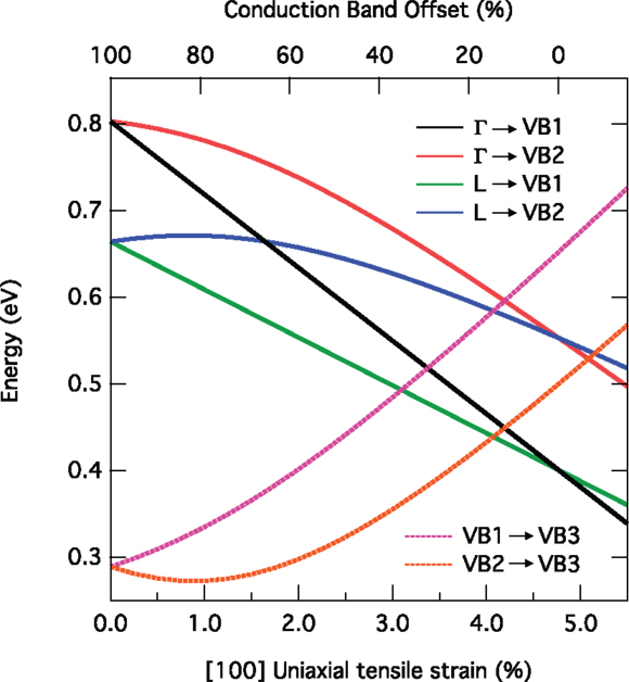
Figure 3. Transition energies between the direct and indirect conduction band valleys and the two top valence bands and within the valence band of uniaxially, tensilely stressed Ge. For a strain of ~4.7%, the conduction band minimum at the Γ-point reaches a lower energy than the indirect L-valleys. The upper x-axis denotes the offset between the Γ- and L-band edges in relative units.
In the valence band, strain lifts the degeneracy of light hole and heavy hole bands and introduces a mixing such that this distinction becomes meaningless, especially under high strain. For low strain, VB1 and VB2 in Figure 3 are mostly “heavy hole”- and “light hole”-like, respectively. VB3 refers to the split-off band. The energetic order of the heavy and light hole bands is reverted when moving from the uniaxial to the biaxial case.
Most of the theoretical work concerning Ge light emission utilizes k·p theory including 6 bands (Aldaghri et al., 2012; Chang and Cheng, 2013; Virgilio et al., 2013), 8 bands (Zhu et al., 2010; Wirths et al., 2013b), or 30 bands (El Kurdi et al., 2010). The latter is not restricted to the Brillouin-zone center but describes the full energy dispersion. In other works, the empirical pseudopotential method (Dutt et al., 2013; Wen and Bellotti, 2015), density functional theory (Tahini et al., 2012), and the tight-binding model (Dutt et al., 2012) are employed. The agreement between the models is generally found to be satisfactory.
Gain
In Figure 4, we show gain calculations for uniaxially stressed Ge in dependence of n-type doping and conduction band offset (c.f. the scale of the upper x-axis in Figure 3). The band structure was computed with an 8-band k·p approach (Birner et al., 2007). The gain was calculated via Fermi’s golden rule, assuming cylindrical symmetry for the valence bands to simplify the calculation of the joint density of states (JDOS), c.f. Virgilio et al. (2013). More details of the calculation can be found in Süess et al. (2013), supplementary information. The peak gain at room temperature (RT) is plotted after subtraction of the loss following the experimentally determined electron- and hole-absorption cross-sections from Carroll et al. (2012) (Süess et al., 2013). The black, broken line indicates when transparency is reached. As an example, for a system at the crossover to a direct band gap system, transparency is nearly reached at a low injection of 1 × 1018 cm−3 as depicted in Figure 4A. Applying a moderate doping of 1 × 1019 cm−3 results in a gain of >500 cm−1, which is sufficient to overcome typical resonator losses. When the doping level is increased to 2 × 1019 cm−3, the gain approximately triples to ~1500 cm−1 according to our model. This suggests that n-doping is a very effective method to promote high gain for correspondingly low excitation in direct band gap systems. This is due to the fact that as long as the offset is not much larger than kT (Sukhdeo et al., 2014), electrons will nevertheless spread into the L-band from where they cannot contribute to gain.
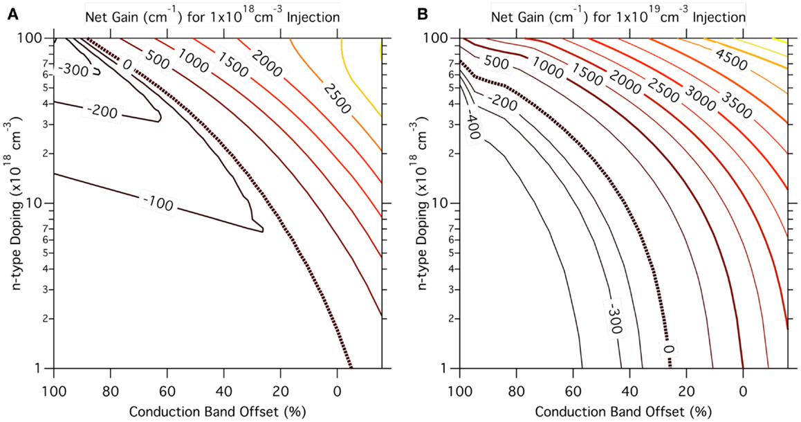
Figure 4. Maximum net gain at room temperature for uniaxially stressed Ge in dependence of n-type doping and conduction band offset. An 8-band k·p model was employed to calculate the band structure parameters. The map is calculated for a carrier injection of (A) 1 × 1018 cm−3 and (B) 1 × 1019 cm−3. The black, broken line depicts the transparency condition when the gain equals the losses.
Transparency can also be achieved for an undoped and still indirect, strained Ge system under higher excitation. We obtain transparency at an injection of 1 × 1019 cm−3 for a system with a remaining offset of 25% (35 meV) and an n-doping level below 1 × 1018cm−3 (see Figure 4B). When the direct band gap is reached (0% offset), the net gain amounts to 1000 cm−1, which can be increased up to 2000 cm−1 at a doping of 2 × 1019 cm−3. In contrast to the indirect band gap Ge, a reduction in temperature helps to increase the gain as soon as the Γ valley constitutes the lowest conduction band energy due to condensation of the carriers into the direct gap states. For example, an intrinsic direct band gap Ge system with 25 meV band offset exhibits a net gain of the order of 4500 cm−1 at a temperature of 20 K and an injection of 1 × 1019 cm−3 compared to 1700 cm−1 at RT.
When comparing gain predictions in literature, we experience larger differences than between predictions of energy levels and their relative positions. The reason for this stems from the uncertainty in the loss. For weakly strained and relaxed Ge, experimental values are available as discussed in Section “Lifetime, Gain, and Loss.” Hence, the overall agreement of the predictions is largely coherent. For example, calculations consistently predict gain for Ge with a large offset (80%) only for the case of very high doping of >5 × 1019 cm−3. For strained and alloyed systems, however, the interband energies approach the one of the intervalence band transitions. The energies may even cross, as shown in Figure 3. Hence, loss processes related to these transitions will become critical. Furthermore, the gain as predicted by a Green’s functional approach (Wen and Bellotti, 2015) tend to be smaller than the commonly used joint density of state formalism as applied for Figure 4.
Fabrication
Microbridges
Strain engineering is nowadays a standard tool in microelectronics to improve device performance, where the lattice mismatch between Si and Ge is used to generate strain via epitaxy. However, the pseudomorphic deposition of Ge on Si leads to compressive strain, which deteriorates the light emission efficiency and is, furthermore, limited to small layer thicknesses. Therefore, the main method used to introduce strain is the application of external stressor layers, such as silicon nitride (SiN), which is compatible with CMOS processing. Some work following this approach includes the deposition of stressors on the back side of Ge membranes (Nam et al., 2011, 2012), on micropillars (Velha et al., 2013), or on selectively grown Ge (Oda et al., 2013).
An advantage of using external stressor layers is the simplicity to combine the strain transfer with standard cavity structures like FP waveguides (Capellini et al., 2014). However, the achieved strain is so far limited to a predominantly uniaxial strain of 1.5%. In other efforts, SiN layers were deposited on Ge microdisks, resulting in a biaxial strain of 1.0% (Ghrib et al., 2013) and 1.5% (Ghrib et al., 2015). However, these stressor layer approaches suffer from a large strain inhomogeneity across the Ge layer, and elaborated all-around stressor techniques using wafer transfer and bonding. These results are included in Figure 2.
Following a different route, it was shown that high levels of tensile strain can be locally induced without the use of any external stressor layers (Minamisawa et al., 2012; Süess et al., 2013). In the approach by Süess et al., the starting substrate is the commonly used tensilely strained Ge layer with a biaxial strain of ~0.2%. Subsequently, the layer is patterned into a microbridge with a narrow central cross-section (the “constriction”) and larger outer cross-sections (the “pads”) as shown in Figures 5A,B. As last processing step, the structure is underetched by selectively removing the underlying buried oxide with hydrofluoric acid, c.f. Figure 5C. Releasing the structure leads to a relaxation of the strain in the pads, which in turn increases the strain in the constriction. Due to Hooke’s law and force balance, strain accumulated in the constriction will depend on the ratio of pad and constriction widths as well as the ratio between their lengths (Minamisawa et al., 2012; Süess et al., 2013). Hence, following this principle, any strain can be generated in the constriction by solely varying the geometrical parameters independent of the actual dimensions of the structure. In contrast to external stressors where the achievable strain is limited by the efficiency of strain transfer, this strain enhancement is only limited by the material strength. Figure 5A shows enhancement factors of more than 20× realized from 0.15% biaxial strain in Ge on Si (blue squares) or Ge on silicon-on-insulator (SOI) (green circles and red triangles) for bridges with varying geometrical dimensions. The agreement of the experimental values with the ones predicted by finite element modeling (red triangles) is excellent. For Ge on SOI, the highest strain achieved in 6 μm × 2 μm constrictions is 3.1%. When starting from 200 nm thick germanium-on-insulator substrates (GOI), which feature a significantly reduced dislocation density (Akatsu et al., 2006; Hartmann et al., 2010), a strain of 5.7% was observed in a 5.0 μm × 0.2 μm constriction (Sukhdeo et al., 2014). According to Figures 2 and 3, such a strain is by far sufficient to transform Ge into a direct band gap material showing the prospect of the strain-enhancement technique given a starting material with high-crystal quality.
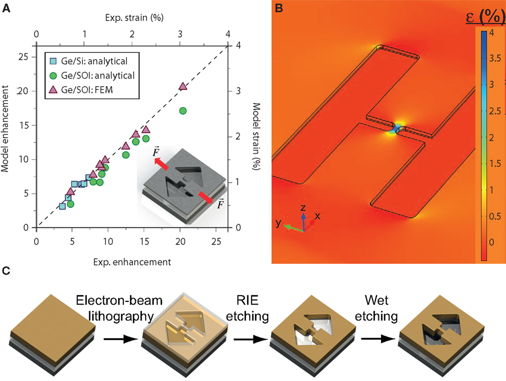
Figure 5. Suspended microbridges from thermally pre-strained Ge. (A) Experimental and modeled strain for Ge microbridges fabricated on Si and SOI. The analytical strain-enhancement model is given in Süess et al. (2013). The enhancement of 22× corresponds to 3.1% uniaxial strain (Süess et al., 2013). (B) Strain profile of a suspended bridge structure as obtained by finite element modeling (FEM). Due to the relaxation in the pads, the strain in the central constriction is enhanced. (C) Process flow for the fabrication of suspended microbridges.
GeSn Alloying
The epitaxial growth of GeSn alloys poses several challenges, such as a large lattice mismatch between α-Sn and Si (17%) or Ge (15%), and a low solid-solubility of <1%. Therefore, the fabrication of high quality and smooth epilayers was a demanding task for many years and the development of new growth processes to deposit GeSn under non-equilibrium conditions at low temperatures was required. Whereas the first attempts to grow GeSn alloys were based on molecular beam epitaxy (MBE) in 1980s and 1990s (Pukite et al., 1989; Harwit et al., 1990; Wegscheider et al., 1990; Fitzgerald et al., 1991; He and Atwater, 1997), device-grade GeSn epilayers could be synthesized since the early 2000s when the first chemical vapor deposition (CVD) processes were developed (Bauer et al., 2003).
Nowadays, several groups established growth processes for GeSn utilizing either MBE (Bratland et al., 2003; Chen et al., 2011a; Bhargava et al., 2013; Oehme et al., 2013) or CVD (Vincent et al., 2011; Chen et al., 2013b; Wirths et al., 2013a; Xu et al., 2013; Du et al., 2014) for a variety of applications, e.g., photodiodes, photodetectors, or MOSFETs. Here, due to the reduced lattice mismatch compared to Si, Ge is preferred as virtual substrate (VS) in order to ensure layers of high monocrystalline quality. Regarding the epitaxial growth of direct band gap GeSn alloys, nearly strain relaxed or even tensilely strained layers are highly desired, since for compressively strained GeSn layers, i.e., GeSn coherently grown on Ge VS, higher Sn contents are necessary for the indirect to direct transition (Gupta et al., 2013b). Owing to an advantageous relaxation mechanism for GeSn layers on Ge VS, dislocations seem to mostly protrude into the Ge VS rather than into the GeSn layer, which is beneficial for optical properties as the density of non-radiative recombination centers is reduced (Takeuchi et al., 2006; Senaratne et al., 2014; Wirths et al., 2015). Although relaxation takes place, a certain level of compressive biaxial strain (typically between −0.6 to −0.8%) remains nevertheless, which, as already said in connection with Figure 2, shifts the indirect-to-direct band gap crossover to higher Sn concentrations with respect to fully relaxed GeSn. Therefore, several approaches are being followed to reduce the compressive strain, such as growth on lattice-matched InGaAs VS (Chen et al., 2011a), which is not acceptable within a CMOS processing line, or deposition of ever thicker layers to enforce further strain relaxation (Senaratne et al., 2014; Wirths et al., 2015). Gupta et al. (2013b) introduced a robust etching approach enabling to selectively dry etch the Ge VS underneath the epitaxial GeSn layers. The authors envision their method to enable the fabrication of direct band gap GeSn micro disks.
Figures 6A–C show transmission electron microscopy images of a GeSn layer with 13% Sn grown via reduced pressure CVD on a Ge VS (Wirths et al., 2015). The advantageous relaxation mechanism mentioned above can be seen here with dislocation-loops (blue arrows) emitted into the Ge VS. Despite the high-Sn content, the thickness of the GeSn layer could be increased up to 560 nm without deteriorating the high-crystalline quality. Owing to the large thickness, a relaxation of 60% could be achieved such that only a mild compressive strain of −0.6% was present. As will be shown in Section “Photoluminescence – Direct Band Gap,” this epilayer was proven to be a direct band gap group IV semiconductor that provides net gain and, hence, shows lasing under optical pumping.
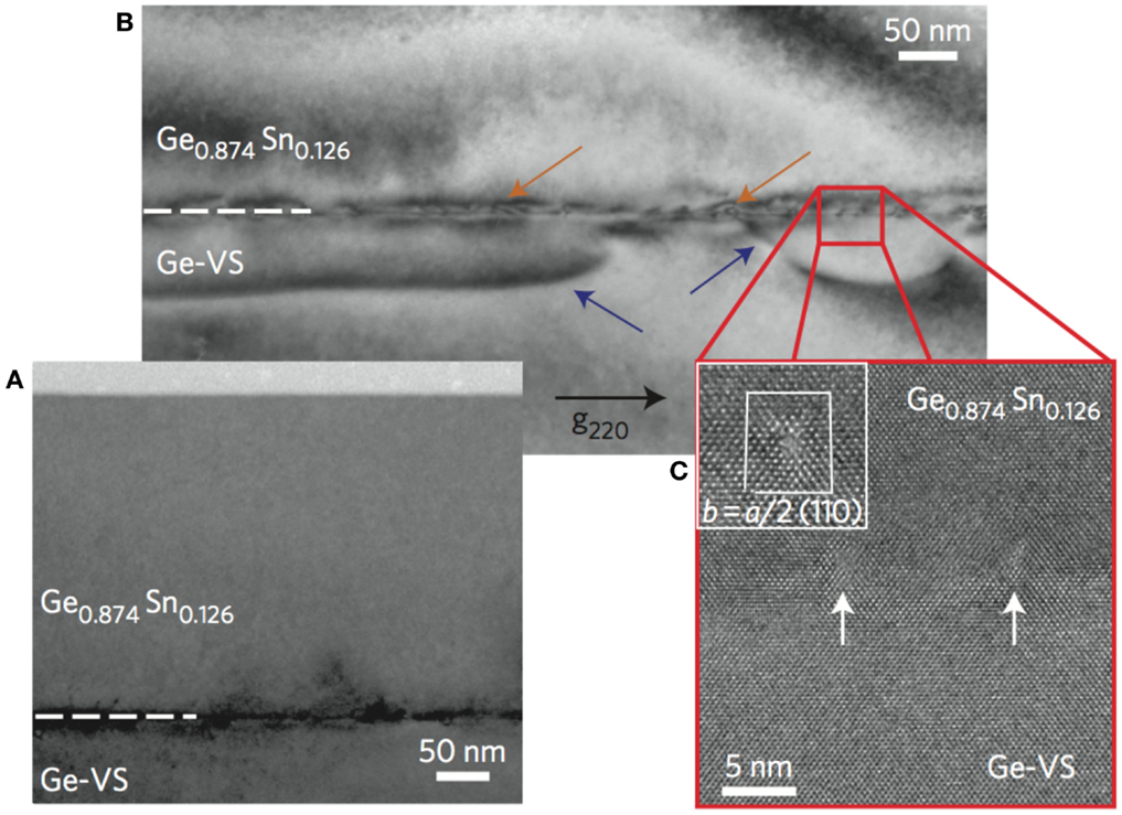
Figure 6. Cross-sectional transmission electron microscopy (TEM) image of a Ge0.87Sn0.13 alloy. (A) Expanded view showing the high-crystalline quality of the GeSn epilayer. The defects are located near the interface to the Ge virtual substrate. (B) Dislocation-loops (blue arrows) emitted below the GeSn/Ge-interface (orange arrows) penetrating only into the Ge virtual substrate. (C) High-resolution TEM image of the interface used for Burgers vector calculations. Lomer dislocations with b = a/2[110] are observed (Wirths et al., 2015).
We conclude this section on the fabrication of GeSn alloys by summarizing the list of beneficial assets GeSn epitaxy brings to the current Si technology facilitating future developments and integration. Apart from the prospect to fabricate a fundamental direct band gap group IV material, GeSn alloys are attractive because of (i) low-temperature deposition on Si(001) compatible with existing CMOS processes; (ii) strain relaxation with reasonably low threading dislocation density; (iii) available option for selective growth on silicon, which is attractive for photonic integration; (iv) GeSn/SiGeSn heterojunction layers to generate carrier confinement in quantum wells; (v) and therefore, tunability of the lattice constant offering opportunities to combine the alloys with the strained membrane method.
Characterization Methods: Optical Properties
Lifetime, Gain, and Loss
When describing a material with regards to its suitability as an efficient laser source, key properties that decide upon adequacy are the gain and loss, i.e., the material’s ability to amplify light, as well as the non-radiative lifetime, which determines the internal quantum efficiency as well as the achievable steady-state carrier density. These characteristics can be extracted in a direct way using broadband, time-resolved pump–probe transmission, and reflection spectroscopy. Possible ways for performing such experiments could be via tunable lasers or supercontinuum sources. However, particularly synchrotron-based infrared pump–probe spectroscopy has been shown to offer advantageous conditions for measuring the carrier density, their lifetime as well as gain and loss due to its extended bandwidth and suitable pulse lengths (Carroll et al., 2012; Geiger et al., 2014a,b). At the infrared beamline of the SLS, 100 ps long pulses of infrared light are supplied from the synchrotron and serve as broadband probe pulses, whereas the excess charge carriers are optically excited by a 100 ps Nd:YAG laser at 1064 nm (Carroll et al., 2011). The delay time between pump and probe pulses can be varied electronically, which offers the possibility to follow the dynamics of a system over a long time period by probing at different times after excitation. In the following, we review some of the pump–probe measurements performed at the SLS and give the most important results that challenge the interpretation of the Ge-lasing observations. We renarrate this discussion at the end of this chapter.
Figure 7A shows the mid-infrared reflection of a Ge layer grown on Si plotted as the ratio of pumped (RP) and unpumped (RU) reflection signal. The different colors depict different optical excitation strengths between 1 and 160 MW cm−2. All of the spectra were taken for a pump–probe delay time of 250 ps. The distinct minimum observed in the spectra is attributed to the carriers’ plasma frequency. For an increasing excitation power, the minimum shifts to higher energy and becomes at the same time more pronounced. As the plasma frequency shifts in first order proportional to the square root of the total amount of charge carriers in the system, such reflection measurements facilitate a convenient method for the quantitative determination of the carrier density. Thus, the extracted carrier concentration in dependence of the optical pump power for delay times of 0 and 250 ps is shown in the inset of Figure 7A. Moreover, by analyzing the carrier density at a fixed pump power for varying delay times, the reflection spectra can be used to extract the carrier decay times. In the case shown here, the carrier density drops to ~4 × 1019 cm−3 within 250 ps for all generated carrier concentrations larger than 4 × 1019 cm−3. This behavior indicates an increasingly faster decay time at high-carrier concentrations, which is attributed to Auger recombination (Carroll et al., 2012).
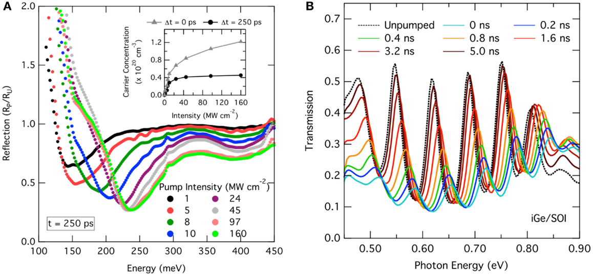
Figure 7. Time-resolved infrared reflection and transmission spectroscopy: (A) mid-infrared reflection spectra of Ge on Si expressed as the ratio of pumped (RP) and unpumped reflection (RU) for varying excitation power at a pump–probe delay of 250 ps. The resonance in the spectra is attributed to the carrier plasma frequency, which enables to extract the total amount of charge carriers. The inset shows the carrier concentration for 0 and 250 ps delay time in dependence of the excitation power. (B) Normal-incidence pump–probe transmission spectra for Ge on SOI for varying delay times. Strong Fabry–Perot oscillations are observed from the thin film interference. Analyzing the peak-shifts facilitates the extraction of the decay time.
While the analysis of mid-infrared reflection spectra enables to directly access charge carrier concentration and decay time, the latter can also be extracted from near-infrared transmission measurements. In Figure 7B, normal-incidence transmission spectra of intrinsic Ge are plotted, while the delay time between pump and probe is varied. As SOI is used as substrate, distinct FP oscillations are observed due to standing wave interferences between the Ge/air and Si/SiO2 interfaces. For short delay times, the transmission is significantly reduced due to absorption. Above the direct band gap of ~0.8 eV, there is an increase compared to the unpumped transmission due to gain or bleaching. By following the shifts of the minima or maxima, the dynamics of the refractive index is obtained, which enables the extraction of the carriers’ decay time. Compared to the decay time analysis from the mid-infrared reflection, the sensitivity to detect small carrier densities is higher in such a measurement because the refractive index – and, hence, the oscillation extrema – follows the carrier densities linearly, which enables to follow the decay processes within an extended time window.
In Figure 8, the time-dependent FP peak shifts are shown for differently prepared Ge layers. The shifts were normalized to unity at t = 0 ns and the decay fitted to an exponential curve (Geiger et al., 2014a). The defective Ge/Si interface was identified as the main non-radiative loss channel, as (i) Ge selectively grown via ultrahigh vacuum CVD (selGe in Figure 8) and a full epilayer grown via low-energy plasma-enhanced CVD (iGe in Figure 8) feature the same surface recombination velocity (SRV) – i.e., the carrier lifetime normalized to the layer thickness – of ~800 m s−1, (ii) a built-in field introduced by modulation doping (nGe/iGe) increases the lifetime compared to iGe by keeping electrons away from the interface, and (iii) the longest lifetime was observed for an overgrown GOI wafer, where the defective Ge/Si interface is removed (SRV = 490 m s−1). These results demonstrate the importance of engineering the material- and, in the case of Ge on Si, especially the interface quality to obtain a high-internal quantum efficiency and, thus, a low-threshold laser. Furthermore, similar pump–probe transmission studies on strained microbridges showed that neither strain, at least up to ~2%, nor processing affects the lifetime (Geiger et al., 2014b), indicating that a high-crystal quality can be maintained using the microbridge strain-enhancement technology.
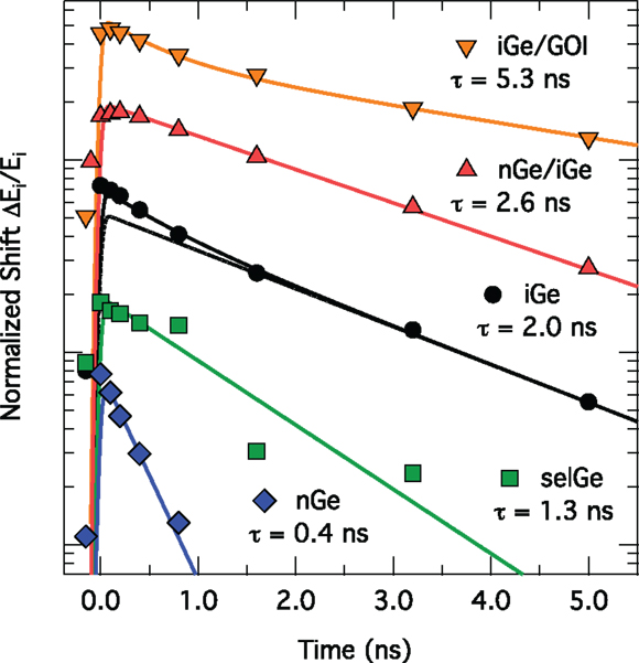
Figure 8. Normalized peak shifts taken from normal-incidence transmission spectra (as, e.g., in Figure 6B) for a series of differently prepared Ge layers: iGe, nGe, selGe refers to intrinsic, n-doped, and selectively grown Ge, respectively. GOI refers to Ge on insulator. The non- radiative lifetime is obtained through an exponential fit to the data (Geiger et al., 2014a).
For the analysis of gain and loss, the transmission spectra should be recorded under the Brewster angle such that the obstructing FP resonances do not occur, c.f. Figure 9A for the case of unstrained Ge on Si for different pump–probe delay times. Δt = 0 ps refers to the maximum overlap between pump and probe and, hence, to the highest carrier density. The thick lines in blue and red show modeled transmission spectra for the unpumped and pumped case. Under excitation, a strong absorption occurs with a linear dependence on energy. At the direct band gap, the absorption gets reduced due to gain, but the gain is too small to generate a negative absorption and, hence, light amplification. This situation holds true for all other delay times, i.e., carrier concentrations, as well.
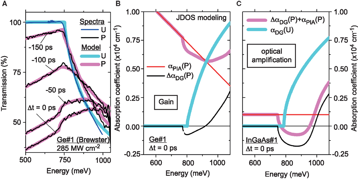
Figure 9. Analysis of pump and probe measurements. (A) Transmission spectra for Ge on Si measured under Brewster angle for different delay times. (B) Modeled direct gap absorption unpumped (blue, thick line) and pumped (red, thick line) as well as pump-induced absorption (red, thin line) obtained from the spectra in (A) at 0 time delay. (C) Similar extraction of direct gap gain and losses for undoped InGaAs showing light amplification, as the gain surpasses the pump-induced losses (Carroll et al., 2012).
In Figure 9B, the situation for Δt = 0 ps is shown again in terms of the absorption coefficient with the modeled functions being plotted separately for (i) direct gap absorption before pumping (blue, thick line), (ii) direct gap absorption under excitation (red, thick line), and (iii) the featureless pump-induced absorption decreasing linearly in energy (red, thin line). Even though a gain of ~850 cm−1 is observed as displayed by a negative absorption, the loss from that spectrally distributed absorption at the same energy is >6000 cm−1 making light amplification impossible. To show the contrast to an established laser material featuring a direct band gap, the same absorption properties are plotted in Figure 9C for the case of InGaAs. Here, the pump-induced losses are independent on energy and amount to ~1000 cm−1, which is compensated by a direct gap gain of ~1700 cm−1 such that a net gain of 700 cm−1 is revealed. We should mention here that the theoretical analysis of Carroll et al. (2012) has been questioned (Dutt et al., 2012) concerning the strength of the gain (red line, Figure 9B) but not the experiments, which clearly show that the loss is by far larger than the gain.
From the preceding analysis, it is clear that a solid understanding and consideration of the loss processes is required for an accurate description of gain in Ge. For illustration, the absorption cross-sections for three Ge samples (Ge#1: Nd = 0, εxx = 0; Ge#2: Nd = 2.5 × 1019 cm−3, εxx = 0; Ge#3: Nd = 0, εxx = 0.25%) are plotted in Figure 10 in dependence of the total carrier density NT = Nd + NP, where Nd refers to the doping concentration and NP to the pump-induced carrier density. As a comparison, the cross-sections of three InGaAs layers (InGaAs#1: Nd = 0, InGaAs#2: Nd = 5.3 × 1018 cm−3; InGaAs#3: Nd = 2.1 × 1019 cm−3) are plotted as well. Therefore, Figure 10 reveals that the absorption scales predominantly with NP indicating that the absorption cross-section from holes σh is much larger than the cross-section for electrons σe. Indeed, describing the absorption via a linearly dependent cross-section as α = σeNe + σhNh (where subscripts e and h refer to electrons and holes, respectively) offers a good representation of the experimental data with σh/σe > 10. The absorption cross-section for holes is significantly larger than for electrons, because in addition to the non-momentum conserving intraband or Drude-type free carrier absorption, the holes can undergo vertical intervalence band transitions (Newman and Tyler, 1957), which are hereby identified as the main loss channel in Ge. A similar conclusion concerning the cross-section ratio can be deduced from the InGaAs data shown in Figure 10 in agreement with common knowledge for direct band gap lasing materials (Adams et al., 1980; Childs et al., 1986). Furthermore, the absolute values of the hole cross-section are in a similar range but larger for InGaAs than for Ge, c.f. Figure 10. However, the absorption is much higher in Ge due to a much larger total carrier density needed to achieve a gain like in the InGaAs sample.
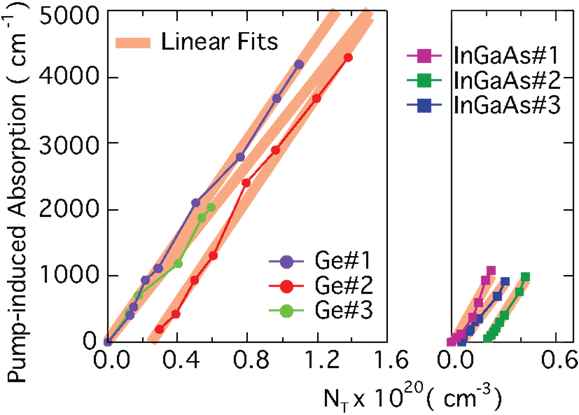
Figure 10. Absorption coefficients for differently doped and strained Ge and InGaAs layers. The data are well described with a linear absorption cross-section model.
Finally, we would like to relate the above presented data of gain and loss as well as of lifetimes in Ge layers on Si to the observation of lasing in highly n-doped and weakly strained Ge (Liu et al., 2010; Camacho-Aguilera et al., 2012), which was recently repeated at the University of Stuttgart with an unstrained, highly n-doped light emitting diode (LED) (Koerner et al., 2015). First, as is shown above by the gain and loss experiment (Carroll et al., 2011), the loss in Ge layers strongly exceeds the gain at all the investigated carrier densities up to 1020 cm−3 and in all investigated cases, i.e., Ge with and without weak strain and/or n-doping. Hence, Carroll’s results are apparently in conflict with the observation of lasing (Liu et al., 2010) in similar but not identical material. Second, the non-radiative lifetimes, which have been determined for such Ge layers only recently by Geiger et al. (2014a), c.f Figure 8, shine a new light on previous and recent gain and threshold current density calculations (Dutt et al., 2012; Peschka et al., 2015). Using the obtained carrier lifetime of the order of 1–2 ns for threshold current estimates, the calculated threshold of the order of 100 kA cm−2 – obtained by assuming a lifetime of 100 ns – needs to be rescaled by a factor of 50–100. Surely, such a current density is above the material’s limit and also exceeds the observed threshold values by ~2 orders of magnitude. Therefore, not only the gain/loss experiments but also the theory (when fed with properly valued parameters) shows that more research is needed to understand the MIT results. The recent paper by the Stuttgart group (Koerner et al., 2015) may give the directions for further thinking: a “lasing” threshold was reached only shortly before their devices failed, hinting at a carrier breakthrough. The heat pulse related to the breakthrough may have caused the peaked emission signal.
Photoluminescence – Direct Band Gap
Photoluminescence spectroscopy offers a convenient tool for probing the changes of the electronic band structure induced via strain or Sn alloying. As shown in Figure 11A, the reduced offset between Γ- and L-valleys manifests in an increased emission intensity of the PL signal (Süess et al., 2013). A similar effect has also been observed by Chen et al. (2011a).
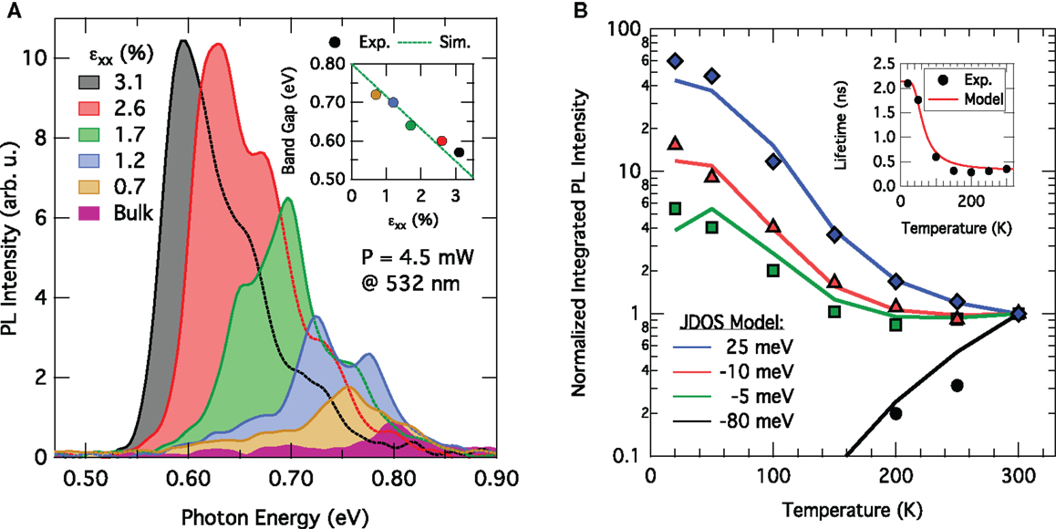
Figure 11. Photoluminescence investigation of strained Ge and GeSn alloys. (A) Room-temperature PL spectra for Ge samples with increasing uniaxial strain up to 3.1%. The inset shows the good agreement between the experimental and modeled band edges. (B) Temperature-dependent integrated PL intensity normalized to unity at 300 K for a series of GeSn layers with Sn-content ranging from 8 to 13%. An increase in Sn-concentration leads to a more pronounced increase in intensity. The offset between Γ- and L-valleys is extracted from JDOS modeling (solid lines), which reveals Ge0.87Sn0.13 to have a fundamental, direct band gap. The inset shows the experimentally extracted non-radiative lifetime modeled with a Shockley–Read–Hall-like temperature dependence (red line).
A quantitative analysis of the relative alignment between Γ- and L can be obtained from the temperature dependence of the PL, as has been demonstrated recently in Wirths et al. (2015). In Figure 11B, the temperature-dependent PL intensity for a set of samples with Sn content from 8 to 13% is shown. The data have been normalized to unity at 300 K. For the sample with the lowest Sn content, a rapid drop in intensity on lowering the temperature is observed, whereas for the three other samples a steady increase in intensity can be seen with the intensity increase being dependent on the Sn concentration. Qualitatively, the increase from sample to sample can be explained by the reduced conduction band offset with increasing Sn, whereas cooling down leads to a condensation of the carriers into the lowest energy states such that the direct gap emission either vanishes for indirect band gap materials as sample Ge0.92Sn0.08 because the Γ valley is not populated anymore or increases strongly when the electrons condense at the minimum of the Γ valley. To quantify the band offsets for the set of GeSn samples, the emission efficiency is calculated via a similar JDOS model as the one used for calculating the gain in Figure 4. Therein, the offset ΔE between Γ- and L-valleys as well as the injected charge carrier density Ni represent the free fitting parameters. Furthermore, the temperature dependence of the lifetime is assumed to be identical for all samples and follows the Shockley–Read–Hall (SRH) recombination characteristics (Shockley and Read, 1952; Schubert, 2006) that describes non-radiative recombination via trap states. Using this model, an excellent agreement with the experimental data is obtained (Wirths et al., 2015). The GeSn sample with 13% Sn content is, hence, identified as a true direct band gap group IV semiconductor with its Γ-valley being 25 meV below the indirect L-valleys. From the second fit parameter, a RT carrier density Ni of 4 × 1017 cm−3 is deduced consistent with a carrier lifetime of 0.35 ns, which corresponds to a SRV of 570 m s−1. This value is close to the ones reported for elemental Ge on Si (Geiger et al., 2014a), c.f. Figure 8, which is an indication of the high-crystalline quality of the investigated GeSn epilayers.
The temperature dependence of the non-radiative carrier lifetime is obtained as:
where τ0 describes the lifetime at low temperature, and τSRH describes the decay due to the capture of charge carriers by mid-gap states, i.e., τSRH = A × (1 + cosh(ET/kT)). τAuger describes the Auger recombination time, which can be neglected here due to the low-carrier densities. Furthermore, ET is the difference between the trap level energy and the intrinsic Fermi-level, k is the Boltzmann constant, and A is to normalize τ to 0.35 ns at 300 K as obtained from the temperature-dependent PL. For ΔE = 19 meV and τ0 = 2.1 ns, a good agreement between the extracted lifetimes and the lifetime model is obtained (Wirths et al., 2015). For temperatures >50 K, there is a drastic decrease in carrier lifetime from ~2 ns to 350 ps for higher temperatures. As the temperature dependence of this process is well described via the SRH model, the lifetime decay is attributed to the capture of carriers via mid-gap states originating from defects (Wirths et al., 2015). These defects could potentially be related to defects located at the GeSn/Ge-interface (Geiger et al., 2013; Wirths et al., 2015), but further studies are needed to unambiguously identify the origin of this deterioration and, subsequently, improve the material quality.
Optically Pumped Laser
According to the modeling results shown in Section “Modeling,” a direct band gap Ge-based system should feature a net gain and, hence, enable light amplification at low excitation. In the previous analysis of low-temperature PL on GeSn alloys in Section “Photoluminescence – Direct Band Gap,” a fundamental direct band gap could be identified for a Sn content of 13% in a strain-relaxed layer with 0.7% compressive biaxial strain. To show lasing, a 560-nm epilayer of such Ge0.87Sn0.13 material was grown providing an overlap of 60% for the fundamental transverse electric mode in a 5 μm wide FP cavity (Wirths et al., 2015). For this layer, modal gain could be observed at 20 K via the variable-stripe-length (VSL) method under pulsed optical excitation at 1064 nm with a differential gain of ≈0.4 cm kW−1 and a threshold excitation density of ≈325 kW cm−2 (c.f. Figure 12). Above threshold, the gain increases linearly with excitation and can easily pass 100 cm−1. The stripe length-dependent PL analysis is a widely applied technique to measure net modal gain, but it does not allow to resolve the gain and loss as by pump and probe spectroscopy. More evidentially, a gain statement, such as provided by Figure 12, becomes respected only after showing lasing.
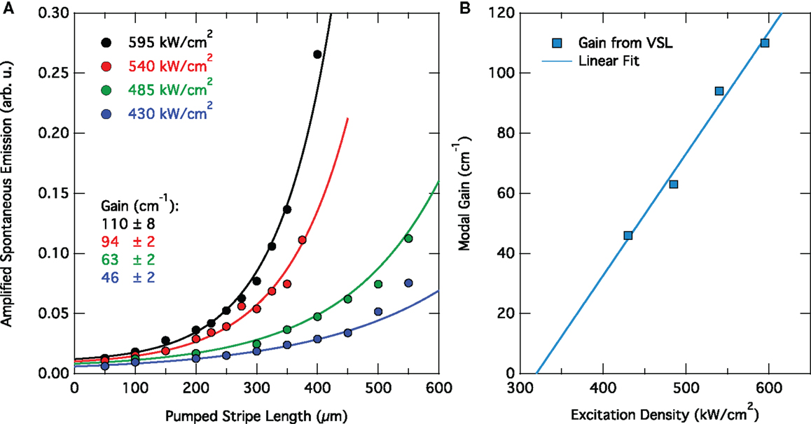
Figure 12. Gain extraction via the variable-stripe-length method (VSL). (A) Edge-emitted intensity of Ge0.87Sn0.13 at 20 K in dependence of the pumped waveguide length for varying excitation densities. The modal gain is extracted by an exponential fit to the data. (B) Differential gain extracted from the spectra in (A) indicating a linear dependence on excitation density with a threshold at 325 kW cm−2.
Indeed, when pumping a FP cavity over its full length, a strongly enhanced emission and narrowing of the line spectra is observed as soon as the modal gain surpasses the cavity losses. This behavior is shown in Figure 13 where the edge-emission spectra from a 1-mm long FP cavity at 20 K are plotted for varying optical excitation powers. The curves are offset for clarity. The threshold obtained from the lasing experiments matches well with the one obtained from the VSL method. For an excitation density of 1 MW cm−2, lasing could be observed up to 90 K. This temperature is equivalent to the temperature range where the lifetime was found to drop substantially from ~2 ns to 350 ps. Hence, it is tempting to attribute the limitation of lasing to temperatures <100 K to the carrier capture by defect-induced mid-gap states, as has appealed from the analysis shown in Figure 11B, inset. However, carrier transfer to the L-valleys and carrier out diffusion into the Ge may be a determining factor, as well.
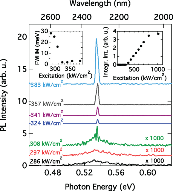
Figure 13. Lasing emission spectra measured from the facet of a 5-μm wide and 1 mm long FP waveguide cavity under optical pumping at 20 K. A clear threshold behavior can be observed in the spectra with respect to output intensity and linewidth, c.f. inset to the right and left hand side, respectively.
Despite the breakthrough of presenting for the first time a direct band gap group IV material that is lasing under optical pumping, there still remain open questions. For example, with an excitation power of 325 kW cm−2, a non-radiative lifetime of 2 ns, as shown in Figure 11, and a typical absorbance of 1 × 104 cm−1 at 1064 nm, a steady-state carrier density of ~3.5 × 1019 cm−3 is estimated. With this number, the gain at low temperature from our model is found to be >5000 cm−1. And, interpolating from Figure 4, at excitation density of 0.6 × 1018 cm−3 we would expect for a system with positive offset of about 15%, a material gain of ~300 cm−1 at RT. We assign this large discrepancy from what is observed at low temperature and what a RT calculation predicts to resonant intervalence band absorption. As mentioned above, due to the lack of experimental data for direct gap Ge or GeSn, the energy dependence of the loss as measured by pump–probe experiments for Ge (Carroll et al., 2012) has been used for Figure 4. Its proper inclusion possibly adds significant contribution to the loss (Wen and Bellotti, 2015).
In order to improve such gain calculations, which critically depend on the knowledge of the band structure, mappings of the entire valence, and conduction band in reciprocal space would certainly be highly valuable. This could be possible via angle-resolved photoelectron spectroscopy (ARPES) at high energy (Gray et al., 2011) or the soft x-ray regime (Strocov et al., 2014). Other promising experimental techniques not covered because of lack of space include lifetime measurements via time-resolved PL measurements (He and Atwater, 1997; Nam et al., 2014; Saito et al., 2014). In fact, similar lifetimes for Ge as obtained from synchrotron measurements (Geiger et al., 2014a) were found (Nam et al., 2014).
Challenges
In the previous section, we reviewed experiments and results related to the dependence of the optical properties on strain and alloying of Ge with Sn. Furthermore, we summarized investigations concerning the first lasing of a direct band gap group IV semiconductor and expounded on the temperature dependence of the PL as a powerful tool to determine the directness of a group IV material. We illustrated optical methods based on pump and probe spectroscopy using synchrotron light to determine the carrier lifetime, gain, and loss under optical pumping related to the injected carrier density.
Future experiments along these lines on both, the strained Ge system and GeSn alloys at various strain and Sn concentration, respectively, will allow to establish the fundamentals of lasing in direct band gap group IV systems. The impact of doping on gain, loss, and carrier lifetime should also be addressed in dependence of the directness of the respective system to verify the picture elucidated by Figure 4 of Section “Gain.”
As an example, intervalence band absorption, Auger recombination, and the electrical injection are some of the many fundamental aspects of group IV direct band gap lasing pending to be understood and quantified.
Intervalence Band Absorption
One of the most essential parameters determining the efficiency of a laser is associated to the parasitic absorption due to the injected holes (Adams et al., 1980; Childs et al., 1986). As shown experimentally by Carroll et al. (2012) for Ge, this absorption depends linearly on the excitation and inclines with decreasing energy. This can be understood from the Drude dependence of the free carrier absorption modified by dipole allowed intervalence band transitions. Because the emission wavelength increases when approaching the direct band gap configuration, and the initially degenerate heavy and light hole bands split due to strain, the parasitic absorption will strongly increase in direct band gap systems and may, thus, obstruct the efficiency of lasing (Wen and Bellotti, 2015). Applying the above introduced optical characterization methods should allow to investigate these effects in detail, which, together with evolving theoretical results, will enable to complete our understanding.
Auger Recombination
On the material level, the performance of optical devices depends strongly on the charge carrier recombination lifetime similarly as described by rate Eq. 1. Here, both the radiative and the Auger recombination lifetime depend on the carrier density n: 1/τrad = B × n, 1/τAuger = C × n2. The quadratic carrier density dependence implicates that Auger recombination becomes a dominant loss mechanism at high-charge carrier densities, which can be the order of >1019 cm−3 for typical laser devices.
Extensive theoretical work based on perturbation theory has shown that, despite its indirect band gap, the band structure of both, Si and Ge, is favorable for direct Auger recombination (Huldt, 1974; Lochmann, 1978) with Auger recombination coefficients of the order of 10−30 cm6s−1. This is comparable to direct band gap materials like GaAs or GaN used for optical devices in the visible part of the spectrum but still much smaller than for low band gap materials like InAs (Metzger et al., 2001).
Significantly, less is known about direct band gap group IV Auger recombination. For direct band gap Ge0.9Sn0.1/Ge0.75Si0.1Sn0.15 multi-quantum-well structures, Sun et al. recently showed theoretically that the RT Auger recombination lifetime is of the order of 50 ns compared to a radiative lifetime of 10 ns (Sun et al., 2010). Other work on GeSn (Dutt et al., 2013) and n-doped or tensile strained Ge (Liu et al., 2007; Jain et al., 2012) only refers to unstrained bulk Ge recombination coefficients to include in their gain models.
We believe, however, that this is unjustified considering that there is an exponential dependence of the Auger lifetime on the band gap and effective masses (Beattie and Landsberg, 1959; Huldt, 1971; Adams et al., 1980), both being strongly altered in direct band gap Ge. Using the simple exponential dependence derived by Beattie and Landsberg (1959) to scale the experimentally determined Auger recombination coefficient of CGe = 10−30 cm6s−1 (Carroll et al., 2012) via the effective masses and band gaps of direct band gap Ge, an Auger coefficient of the order of 10−26–10−27 cm6s−1 is obtained. Despite the overly strong simplicity of this comparison, it shows that Auger coefficients will most probably increase and need to be addressed and investigated in the future.
Carrier Injection
From an electronic point of view, Ge is one of the most interesting materials as it offers both, high electron and hole mobilities (μe = 3900 cm2/Vs and μh = 1900 cm2/Vs, respectively) (Golikova et al., 1962; Jacoboni et al., 1981). For optical devices, this is appealing because it results in diffusion lengths of several 100 μm, more than sufficient for, e.g., typical detector absorber sizes and laser cavity lengths. However, at the same time, Ge suffers from its low band gap, which causes large leakage currents in Ge pn junctions (Metzger et al., 2001; Satta et al., 2006), thus, requiring extensive work on surface passivation due to the lack of a native oxide.
The already beneficial mobility properties can be further improved by employing tensile strain as has been shown for both, uniaxially and biaxially strained Ge (Schetzina and McKelvey, 1969; Chu et al., 2009; Chen et al., 2011b). Here, we would like to highlight that all these studies have been performed on indirect band gap Ge where the increase in electron mobility is mediated by a reduction of the effective mass in the L valley. Even without strain, the Γ-valley already offers an ~8 times smaller effective mass and correspondingly higher electron mobility. Similarly, an increase in hole mobility is expected due to the lifting of the valence band degeneracy (Beattie and Landsberg, 1959; Fischetti and Laux, 1996). This is advantageous as a high mobility strongly reduces the resistivity of the device allowing an efficient injection and extraction of charge carriers.
GeSn emerged as a material of interest in electronics only recently; therefore, less transport data are available. However, theoretical studies predict very large electron mobilities as well as hole mobilities of the order of 4500 cm2/Vs for direct band gap GeSn (Sau and Cohen, 2007). The first reported experimental mobility study has been done on low Sn content (<6%) indirect band gap GeSn layers yielding a Hall mobility of the order of ~200–300 cm2/Vs (Nakatsuka et al., 2010). Slightly better results have been obtained thereafter investigating p-MOSFETs hole channel mobility (Gupta et al., 2013a; Wang et al., 2013).
In summary, we see that a vast amount of knowledge concerning the mobility exists leaving a good base for further studies. Moreover, many electrical devices and the corresponding fabrication techniques, e.g., passivation, contacting, or annealing, have been conceived allowing for a fast implementation in optical devices.
However, besides the tremendous changes in the carrier mobility, there are additional effects coming into play with electrical injection of charge carriers from indirect to direct band gap Ge. Exemplarily in Figure 14, such an injection scheme in form of a pin diode is discussed for the case of tensile strained Ge bridges where the strain profile is shown in Figure 5B.
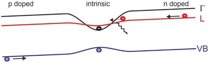
Figure 14. Schematic of the band structure of a forward biased pin strained Ge bridge diode where the intrinsic layer and strained region overlap.
Far from the strained constriction, electrons can be injected into the L-valleys of the conduction band as in standard Ge diodes. However, close to the center the strain profile alters the band structure with L- and γ-valley starting to cross, which allows for intervalley scattering (Boucaud et al., 2013) from a high- into a low-effective mass valley with a higher mobility, a process inverse to the Gunn effect (Gunn, 1963). This may support current extraction and injection in optical devices. However, an actual impact still needs to be proven.
Cavity Design
For the usage of direct band gap materials in lasing structures, high-quality factor optical resonators are necessary confining the light in the gain region and, thus, allowing for stimulated emission. Helpful in this regard is the high-refractive index contrast of the Ge–air and GeSn–air interfaces (Kasper et al., 2013), which should allow for good confinement properties. The design of suitable cavities seems to be straightforward for GeSn lasers where the wafer-scale direct band gap on Si or Ge already facilitated the implementation of well-known laser cavities, such as FP cavities (Wirths et al., 2015) or microdisks (Cho et al., 2011). At the same time, optical microdisk cavities with quality factors of ~1400 have been demonstrated in tensile strained Ge using external SiN stressors (Ghrib et al., 2013) as well as waveguide cavities (Capellini et al., 2014).
The situation is much more complex for uniaxially strained Ge bridges where patterning of the bridge inevitably relaxes the strain and, hence, prohibits a fundamental direct band gap. This excludes many popular cavity designs, in particular, microdisks, photonic crystals, and FP cavities. Hence, distributed feedback structures, which do not rely on patterning of the strained region, are currently under investigation (Marin et al., 2015).
Band Gap Renormalization and Material Stability
Relevant for both here discussed direct band gap systems is a quantitative analysis of the band gap renormalization of the involved Γ and L valleys in dependence of their respective carrier population. So far, experiments suggest that the renormalization corrections are comparable for the two valleys. Hence, the offset between the Γ and L states would not depend on the injection density, which is essential for a stable injection.
Moreover, material specific investigation concerns, for example, the thermal stability of GeSn and SiGeSn metastable alloys with regards to Sn diffusion and segregation where extensive segregation can result in changes of the emission wavelength and/or emission efficiency. Recently, investigations have been pursued to examine the temperature budget a GeSn or SiGeSn device would be able to withstand, e.g., by in situ studies (Fournier-Lupien et al., 2014) or annealing experiments (Wirths et al., 2014). First, in situ results indicate phase separation of a 12% Sn containing ternary SiGeSn and binary GeSn alloys at ~420 and 460°C, respectively, which is surprising considering that the higher mixing entropy usually results in a higher thermal stability of ternary alloys (Fournier-Lupien et al., 2014). Annealing experiments revealed distinct Sn diffusion at 300°C for GeSn with approximately the same composition (Wirths et al., 2014).
Finding the intrinsic stress limits of Ge is another item of interest in this context.
By saying this, we conclude our listing of fundamental and materials-related challenges. This list may be incomplete. However, it confirms that the research and development of a laser source from a group IV material will involve many disciplines from fundamental to device physics and from wave optics to material and transport properties. To progress fast, a collaborative effort is demanded.
Opportunities
Photonics
Direct band gap group IV laser systems may permit a qualitative as well as a quantitative expansion of Si-photonics (group IV photonics) into traditional but also new areas of applications. However, it is requested that such lasers can be operated energy efficiently, under ambient conditions and can be fully integrated with current Si technology. An answer to whether this is possible cannot be given yet as the research is at an early stage. We can only speculate about the specifications of such a laser and, thus, have to guess which of the applications would profit most from a successful implementation of group IV lasers. Hence, for the following discussion, let us assume that this all-group-IV laser does indeed exist and it operates (i) under electrical injection, (ii) at RT or above, and (iii) with reasonable power conversion efficiency. What could we do with such a device, where is the highest impact, and what is the platform of choice?
A high return is merely achievable when this laser device will be combined with the current Si photonics by using the same platform. Most advanced are photonic elements fabricated on SOI, except for applications in the visible part of the spectrum – not covered here – where SiN-based structures are often used. SOI for photonics typically consists of Si layers with a thickness of ~200–250 nm and a several micrometer thick buried oxide to avoid leakage of the propagating modes into the Si substrate. For strain engineering, the compatibility with SOI has already been shown (Süess et al., 2013), c.f. Section “Microbridges,” and, as mentioned above, bridges with even higher mechanical strength are fabricated from GOI using wafer transfer (Sukhdeo et al., 2014). In fact, wafer-scale fabrication of GOI using the SmartCut® process has already been established several years ago for electronics (Augendre et al., 2009). GOI for photonic applications, where thicker layers and a thicker BOX are required, has been presented recently by Reboud et al. (2015). A photonic platform based on GOI, in comparison to SOI, has the advantage that all photonic elements, such as waveguides, bends, and the resonant structures, can be reduced in size because of the larger refractive index contrast. This allows for the potential fabrication of more dense optical circuits and, hence, for an easier integration with electronics. Furthermore, Ge provides coverage of the longer wavelengths toward 10 μm and more. Moreover, by using processes that are selective for either Ge or Si, the GOI platform may provide additional fabrication opportunities. The high quality (Si)GeSn presented by Wirths et al. (2013b) has been deposited on a Ge VS on Si(001) indicating that the growth on SOI and certainly GOI is possible, as well.
With a laser device implemented on the currently used SOI or similarly on GOI, various new applications will emerge. Before speculating, we may picture the many already existing photonic elements. To select a few: Low-loss (<1 dB cm−1) single mode waveguides in various designs, tapers to adiabatically match the waveguide modes to fibers, and low-loss grating couplers (<1 dB) in 1D or 2D providing polarization splitting. Other standard elements include directional couplers, Mach Zehnder interferometers, ring resonators, and light modulators based on free carrier injections or quantum confined Stark effect. Detectors based on slightly tensile strained (0.2%) Ge provide more than 10 GHz speed for high-data rate transmission. Other device elements include add-drop filters, buffers, and switches, which can be integrated with fluidic channels for (bio-) sensing. The short wavelength infrared at which the here discussed group IV direct band gap lasers emit (see Figure 3) is certainly a clear asset for sensing applications (Soref, 2010; Nedeljkovic et al., 2013).
Silicon-on-insulator is (and GOI could become) a very convenient platform to realize high-performing photonic crystal structures enabling unique photonic circuits, such as compact high-Q cavities, which can operate stably at single and dual-wavelength, and as wavelength division multiplexer as desired for optical signal processing. This listing can be extended almost indefinitely, naming, e.g., switching and steering of optical signals, slow light, pulse compression, customized reflectors, and filters. Together with the expectation that such photonic circuits will be very cost effective, compact, reliable, and efficient, a monolithically integrated laser source will certainly bring new functionality, in particular when optics can be merged with electronics.
CMOS Integration
The combination of optics with CMOS electronics to realize an on-chip data distribution network (Heck and Bowers, 2014) is – without any doubt – one of the most advanced and challenging applications for direct band gap group IV lasers. The requirements are so complex (Miller, 2009) that before the start of such a development, many fundamental questions have to be answered, such as the efficiency issues among other challenges, which have been addresses in the previous section. However, once these hurdles are taken, we expect to arise a highly competitive and attractive platform solution for future data processing applications. In fact, the extension of CMOS by integration of Ge and (Si)GeSn may not just resolve the demands for a monolithic laser gain medium, but, as discussed widely elsewhere (Kao et al., 2014), (Si)GeSn would already advance the performance of the electronic circuits. This appealing double benefit, together with the potential compatibility to CMOS of such an all-group-IV solution, bears an essential advantage in comparison to other emerging technologies, such as spin- and/or valley-based electronics, which rely in part on non-conform chemical elements and non-CMOS fabrication processes.
Hence, we expect that as soon as the fundamental lessons of direct band gap lasing are learnt and a gain medium well-qualified for injection pumping at RT is defined, research and development of a new opto-electronic platform will quickly advance. Experts in CMOS technology, group IV epitaxy, laser physics, and Si electronics and photonics will cooperate and define the routes to opto-electronics for fast and energy-efficient data processing.
Conclusion and Outlook
We reviewed the methods for achieving a direct band gap in group IV semiconductors in the most promising material system for the prospect of a Si compatible laser, namely, Ge modified either via tensile strain or by alloying with Sn. We expanded on the methods to characterize these systems and gave examples on their optical properties. The recent advances in numerous approaches to achieve a direct band gap have finally concluded in the first demonstration of lasing in a direct band gap GeSn alloy (Wirths et al., 2015).
With this demonstration, we are at the beginning of an exciting journey in the field of silicon photonics. As shown in great detail, the many optical characterization tools at hand allow us to address a large amount of fundamental questions, including band gap renormalization, various recombination processes, and doping level-dependent lasing performance, but also material- and technology-related issues, such as high Q-factor cavity design, diffusive carrier transport, stress, and thermal diffusion limits.
We hope that with outlining these challenges, we can motivate a vast amount of new researchers from various backgrounds in optics, material science, and device physics to join this interesting research field. We believe that combined efforts will converge in a reasonable time to a demonstration of a practical laser source being electrically pumped, highly efficient, and fully integrated on an electro-optical CMOS platform. This building block will finally pave the way for true monolithic on-chip integration of photonics and CMOS electronics for new sensors in the long wavelength infrared, and will eventually enable to build an on-chip or off-chip electro-optical data distribution network for high-performance computing.
Conflict of Interest Statement
The authors declare that the research was conducted in the absence of any commercial or financial relationships that could be construed as a potential conflict of interest.
Acknowledgments
We would like to acknowledge the many scientific collaborators we were fortunate to work with over the last few years. They supported us in building up a strong portfolio in the investigation and understanding of lasing in group IV systems, and the fabrication of direct band gap group IV materials. In particular, we thank our previous group members Gustav Schiefler, Martin J. Süess, and Renato Minamisawa for their contributions, which led to this appealing strain concept, and the group of Dan Buca (FZ Jülich), who contacted us for investigating their high quality material and thus gave us the opportunity to learn also about GeSn alloys. The tremendous progress achieved in a short time is a shining example of our good collaboration. We also thank Jérôme Faist and Ralph Spolenak (ETHZ) for their whole-hearted support to this subject and their many essential contributions. Finally, we acknowledge the Swiss Science Foundation (SNF) for supporting part of the here reviewed studies over several years.
References
Adams, A. R., Asada, M., Suematsu, Y., and Arai, S. (1980). The temperature dependence of the efficiency and threshold current of In 1- xGa xAs yP 1- y lasers related to intervalence band absorption. Jpn. J. Appl. Phys. 19, L621–L624. doi: 10.1143/JJAP.19.L621
Akatsu, T., Deguet, C., Sanchez, L., Allibert, F., Rouchon, D., Signamarcheix, T., et al. (2006). Germanium-on-insulator (GeOI) substrates – a novel engineered substrate for future high performance devices. Mater. Sci. Semicond. Process. 9, 444–448. doi:10.1016/j.mssp.2006.08.077
Aldaghri, O., Ikonic´, Z., and Kelsall, R. W. (2012). Optimum strain configurations for carrier injection in near infrared Ge lasers. J. Appl. Phys. 111, 053106. doi:10.1063/1.3691790
Augendre, E., Sanchez, L., Benaissa, L., Signamarcheix, T., Hartmann, J.-M., Le Royer, C., et al. (2009). Challenges and progress in germanium-on-insulator materials and device development towards ULSI integration. ECS Trans. 25, 351–362. doi:10.1149/1.3203972
Bauer, M. R., Tolle, J., Bungay, C., Chizmeshya, A. V. G., Smith, D. J., Menéndez, J., et al. (2003). Tunable band structure in diamond-cubic tin-germanium alloys grown on silicon substrates. Solid State Commun. 127, 355–359. doi:10.1016/S0038-1098(03)00446-0
Beattie, A. R., and Landsberg, P. T. (1959). Auger effect in semiconductors. Proc. R. Soc. A Math. Phys. Eng. Sci. 249, 16–29. doi:10.1098/rspa.1959.0003
Bhargava, N., Coppinger, M., Gupta, J. P., Wielunski, L., and Kolodzey, J. (2013). Lattice constant and substitutional composition of GeSn alloys grown by molecular beam epitaxy. Appl. Phys. Lett. 103, 041908. doi:10.1063/1.4816660
Birner, S., Zibold, T., Andlauer, T., Kubis, T., Sabathil, M., Trellakis, A., et al. (2007). Nextnano: general purpose 3-D simulations. IEEE Trans. Electron Devices 54, 2137–2142. doi:10.1109/TED.2007.902871
Boucaud, P., Kurdi El, M., Ghrib, A., Prost, M., de Kersauson, M., Sauvage, S., et al. (2013). Recent advances in germanium emission. Photon. Res. 1, 102. doi:10.1364/PRJ.1.000102
Bratland, K., Foo, Y., Soares, J., Spila, T., Desjardins, P., and Greene, J. (2003). Mechanism for epitaxial breakdown during low-temperature Ge(001) molecular beam epitaxy. Phys. Rev. B 67, 125322. doi:10.1103/PhysRevB.67.125322
Camacho-Aguilera, R. E., Cai, Y., Patel, N., Bessette, J. T., Romagnoli, M., Kimerling, L. C., et al. (2012). An electrically pumped germanium laser. Opt. Express 20, 11316. doi:10.1364/OE.20.011316
Capellini, G., Kozlowski, G., Yamamoto, Y., Lisker, M., Wenger, C., Niu, G., et al. (2013). Strain analysis in SiN/Ge microstructures obtained via Si-complementary metal oxide semiconductor compatible approach. J. Appl. Phys. 113, 013513. doi:10.1063/1.4772781
Capellini, G., Reich, C., Guha, S., Yamamoto, Y., Lisker, M., Virgilio, M., et al. (2014). Tensile Ge microstructures for lasing fabricated by means of a silicon complementary metal-oxide-semiconductor process. Opt. Express 22, 399–410. doi:10.1364/OE.22.000399
Carroll, L., Friedli, P., Lerch, P., Schneider, J., Treyer, D., Hunziker, S., et al. (2011). Ultra-broadband infrared pump-probe spectroscopy using synchrotron radiation and a tuneable pump. Rev. Sci. Instrum. 82, 063101–063101–9. doi:10.1063/1.3592332
Carroll, L., Friedli, P., Neuenschwander, S., Sigg, H., Cecchi, S., Isa, F., et al. (2012). Direct-gap gain and optical absorption in germanium correlated to the density of photoexcited carriers, doping, and strain. Phys. Rev. Lett. 109, 057402. doi:10.1103/PhysRevLett.109.057402
Chang, G.-E., and Cheng, H. H. (2013). Optical gain of germanium infrared lasers on different crystal orientations. J. Phys. D Appl. Phys. 46, 065103. doi:10.1088/0022-3727/46/6/065103
Chen, R., Gupta, S., Huang, Y.-C., Huo, Y., Rudy, C. W., Sanchez, E., et al. (2013a). Demonstration of a Ge/GeSn/Ge quantum-well microdisk resonator on silicon: enabling high-quality Ge(Sn) materials for micro- and nanophotonics. Nano Lett. 14, 37–43. doi:10.1021/nl402815v
Chen, R., Huang, Y.-C., Gupta, S., Lin, A. C., Sanchez, E., Kim, Y., et al. (2013b). Material characterization of high Sn-content, compressively-strained GeSn epitaxial films after rapid thermal processing. J. Cryst. Growth 365, 29–34. doi:10.1016/j.jcrysgro.2012.12.014
Chen, R., Lin, H., Huo, Y., Hitzman, C., Kamins, T. I., and Harris, J. S. (2011a). Increased photoluminescence of strain-reduced, high-Sn composition Ge1−xSnx alloys grown by molecular beam epitaxy. Appl. Phys. Lett. 99, 181125. doi:10.1063/1.3658632
Chen, Y. T., Lan, H. S., Hsu, W., Fu, Y. C., Lin, J. Y., and Liu, C. W. (2011b). Strain response of high mobility germanium n-channel metal-oxide-semiconductor field-effect transistors on (001) substrates. Appl. Phys. Lett. 99, 022106. doi:10.1063/1.3604417
Childs, G. N., Brand, S., and Abram, R. A. (1986). Intervalence band absorption in semiconductor laser materials. Semicond. Sci. Technol. 1, 116–120. doi:10.1088/0268-1242/1/2/004
Cho, S., Chen, R., Koo, S., Shambat, G., Lin, H., Park, N., et al. (2011). Fabrication and analysis of epitaxially grown Ge1-xSnx microdisk resonator with 20-nm free-spectral range. IEEE Photon. Technol. Lett. 23, 1535–1537. doi:10.1109/LPT.2011.2163929
Chow, W. W. (2012). Model for direct-transition gain in a Ge-on-Si laser. Appl. Phys. Lett. 100, 191113. doi:10.1063/1.4714540
Chu, M., Sun, Y., Aghoram, U., and Thompson, S. E. (2009). Strain: a solution for higher carrier mobility in nanoscale MOSFETs. Annu. Rev. Mater. Res. 39, 203–229. doi:10.1146/annurev-matsci-082908-145312
Du, W., Ghetmiri, S. A., Conley, B. R., Mosleh, A., Nazzal, A., Soref, R. A., et al. (2014). Competition of optical transitions between direct and indirect bandgaps in Ge1−xSnx. Appl. Phys. Lett. 105, 051104. doi:10.1063/1.4892302
Dutt, B., Lin, H., Sukhdeo, D. S., Vulovic, B. M., Gupta, S., Nam, D., et al. (2013). Theoretical analysis of GeSn alloys as a gain medium for a Si-compatible laser. IEEE J. Sel. Top. Quantum Electron. 19, 1502706–1502706. doi:10.1109/JSTQE.2013.2241397
Dutt, B., Sukhdeo, D. S., Nam, D., Vulovic, B. M., Ze, Y., and Saraswat, K. C. (2012). Roadmap to an efficient germanium-on-silicon laser: strain vs. n-type doping. IEEE Photon. J. 4, 2002–2009. doi:10.1109/JPHOT.2012.2221692
El Kurdi, M., Fishman, G., Sauvage, S., and Boucaud, P. (2010). Band structure and optical gain of tensile-strained germanium based on a 30 band k·p formalism. J. Appl. Phys. 107, 013710. doi:10.1063/1.3279307
Fang, Z., Chen, Q. Y., and Zhao, C. Z. (2013). A review of recent progress in lasers on silicon. Opt. Laser Technol. 46, 103–110. doi:10.1088/0034-4885/76/3/034501
Fischetti, M. V., and Laux, S. E. (1996). Band structure, deformation potentials, and carrier mobility in strained Si, Ge, and SiGe alloys. J. Appl. Phys. 80, 2234–2252. doi:10.1063/1.363052
Fitzgerald, E. A., Xie, Y. H., Green, M. L., Brasen, D., Kortan, A. R., Michel, J., et al. (1991). Totally relaxed GexSi1−x layers with low threading dislocation densities grown on Si substrates. Appl. Phys. Lett. 59, 811. doi:10.1063/1.105351
Fournier-Lupien, J. H., Chagnon, D., Levesque, P., AlMutairi, A. A., Wirths, S., Pippel, E., et al. (2014). In situ studies of germanium-tin and silicon-germanium-tin thermal stability. ECS Trans. 64, 903–911. doi:10.1149/06406.0903ecst
Geiger, R., Frigerio, J., Süess, M. J., Chrastina, D., Isella, G., Spolenak, R., et al. (2014a). Excess carrier lifetimes in Ge layers on Si. Appl. Phys. Lett. 104, 062106–062106. doi:10.1063/1.4865237
Geiger, R., Süess, M. J., Bonzon, C., Frigerio, J., Chrastina, D., Isella, G., et al. (2014b). Carrier Lifetimes in Uniaxially Strained Ge Micro Bridges. IEEE, 227–228.
Geiger, R., Süess, M. J., Bonzon, C., Spolenak, R., Faist, J., and Sigg, H. (2014c). Strained Ge Microbridges to Obtain a Direct Bandgap Laser. IEEE, 7–8.
Geiger, R., Frigerio, J., Süess, M. J., Minamisawa, R. A., Chrastina, D., Isella, G., et al. (2013). Excess Carrier Lifetimes in Ge Layers on Si. IEEE, 103–104.
Ghrib, A., Kurdi El, M., de Kersauson, M., Prost, M., Sauvage, S., Checoury, X., et al. (2013). Tensile-strained germanium microdisks. Appl. Phys. Lett. 102, 221112. doi:10.1364/OE.23.006722
Ghrib, A., Kurdi El, M., Prost, M., Sauvage, S., Checoury, X., Beaudoin, G., et al. (2015). All-around SiN stressor for high and homogeneous tensile strain in germanium microdisk cavities. Adv. Opt. Mater. 3, 353–358. doi:10.1002/adom.201400369
Golikova, O. A., Moizhes, B. Y., and Stilbans, L. S. (1962). Hole mobility of germanium as a function of concentration and temperature. Sov. Phys. Solid State 3, 2259–2265.
Gray, A. X., Papp, C., Ueda, S., Balke, B., Yamashita, Y., Plucinski, L., et al. (2011). Probing bulk electronic structure with hard X-ray angle-resolved photoemission. Nat. Mater. 10, 759–764. doi:10.1038/nmat3089
Greil, J., Lugstein, A., Zeiner, C., Strasser, G., and Bertagnolli, E. (2012). Tuning the electro-optical properties of germanium nanowires by tensile strain. Nano Lett. 12, 6230–6234. doi:10.1021/nl303288g
Gunn, J. B. (1963). Microwave oscillations of current in III–V semiconductors. Solid State Commun. 1, 88–91. doi:10.1016/0038-1098(63)90041-3
Gupta, S., Chen, R., Vincent, B., Lin, D., Magyari-Kope, B., Caymax, M., et al. (2013a). (Invited) GeSn channel n and p MOSFETs. ECS Trans. 50, 937–941. doi:10.1149/05009.0937ecst
Gupta, S., Magyari-Köpe, B., Nishi, Y., and Saraswat, K. C. (2013b). Achieving direct band gap in germanium through integration of Sn alloying and external strain. J. Appl. Phys. 113, 073707. doi:10.1063/1.4792649
Hartmann, J. M., Sanchez, L., Van Den Daele, W., Abbadie, A., Baud, L., Truche, R., et al. (2010). Fabrication, structural and electrical properties of compressively strained Ge-on-insulator substrates. Semicond. Sci. Technol. 25, 075010. doi:10.1088/0268-1242/25/7/075010
Harwit, A., Pukite, P. R., Angilello, J., and Iyer, S. S. (1990). Properties of diamond structure SnGe films grown by molecular beam epitaxy. Thin Solid Films 184, 395–401. doi:10.1016/0040-6090(90)90437-I
He, G., and Atwater, H. A. (1997). Interband transitions in SnxGe1−xAlloys. Phys. Rev. Lett. 79, 1937–1940. doi:10.1103/PhysRevLett.79.1937
Heck, M. J. R., and Bowers, J. E. (2014). Energy efficient and energy proportional optical interconnects for multi-core processors: driving the need for on-chip sources. IEEE J. Sel. Top. Quantum Electron. 20, 332–343. doi:10.1109/JSTQE.2013.2293271
Huldt, L. (1971). Band-to-band auger recombination in indirect gap semiconductors. Phys. Status Solidi A 8, 173–187. doi:10.1002/pssa.2210080118
Huldt, L. (1974). Auger recombination in germanium. Phys. Status Solidi A 24, 221–229. doi:10.1088/0957-4484/22/43/435401
Huo, Y., Lin, H., Chen, R., Makarova, M., Rong, Y., Li, M., et al. (2011). Strong enhancement of direct transition photoluminescence with highly tensile-strained Ge grown by molecular beam epitaxy. Appl. Phys. Lett. 98, 011111. doi:10.1063/1.3534785
Jacoboni, C., Nava, F., Canali, C., and Ottaviani, G. (1981). Electron drift velocity and diffusivity in germanium. Phys. Rev. B 24, 1014–1026. doi:10.1103/PhysRevB.24.1014
Jain, J. R., Hryciw, A., Baer, T. M., Miller, D. A. B., Brongersma, M. L., and Howe, R. T. (2012). A micromachining-based technology for enhancing germanium light emission via tensile strain. Nat. Photonics 6, 398–405. doi:10.1038/nphoton.2012.111
Kao, K.-H., Verhulst, A. S., Rooyackers, R., Douhard, B., Delmotte, J., Bender, H., et al. (2014). Compressively strained SiGe band-to-band tunneling model calibration based on p-i-n diodes and prospect of strained SiGe tunneling field-effect transistors. J. Appl. Phys. 116, 214506. doi:10.1063/1.4903288
Kasper, E., Kittler, M., Oehme, M., and Arguirov, T. (2013). Germanium tin: silicon photonics toward the mid-infrared [Invited]. Photon. Res. 1, 69. doi:10.1364/PRJ.1.000069
Koerner, R., Oehme, M., Gollhofer, M., Schmid, M., Kostecki, K., Bechler, S., et al. (2015). Electrically pumped lasing from Ge Fabry-Perot resonators on Si. Opt. Express 23, 14815–14822. doi:10.1364/OE.23.014815
Liu, J., Sun, X., Camacho-Aguilera, R., Kimerling, L. C., and Michel, J. (2010). Ge-on-Si laser operating at room temperature. Opt. Lett. 35, 679. doi:10.1364/OL.35.000679
Liu, J., Sun, X., Pan, D., Wang, X., Kimerling, L. C., Koch, T. L., et al. (2007). Tensile-strained, n-type Ge as a gain medium for monolithic laser integration on Si. Opt. Express 15, 11272. doi:10.1364/OE.15.011272
Lochmann, W. (1978). Phonon-assisted auger recombination in indirect gap semiconductors. Phys. Status Solidi A 45, 423–432. doi:10.1002/pssa.2210450208
Low, K. L., Yang, Y., Han, G., Fan, W., and Yeo, Y.-C. (2012). Electronic band structure and effective mass parameters of Ge1-xSnx alloys. J. Appl. Phys. 112, 103715. doi:10.1063/1.4767381
Marin, E., Bonzon, C., Geiger, R., Zabel, T., Sigg, H., and Faist, J. (2015). Proceedings CLEO-Europe 2015. (in print)
Metzger, W. K., Wanlass, M. W., Ellingson, R. J., Ahrenkiel, R. K., and Carapella, J. J. (2001). Auger recombination in low-band-gap n-type InGaAs. Appl. Phys. Lett. 79, 3272–3274. doi:10.1063/1.1418032
Michel, J., Liu, J., and Kimerling, L. C. (2010). High-performance Ge-on-Si photodetectors. Nat. Photonics 4, 527–534. doi:10.1038/nphoton.2010.157
Miller, D. A. B. (2009). Device requirements for optical interconnects to silicon chips. Proc. IEEE 97, 1166–1185. doi:10.1109/JPROC.2009.2014298
Miller, D. A. B. (2010). Optical interconnects to electronic chips. Appl. Opt. 49, F59. doi:10.1364/AO.49.000F59
Minamisawa, R. A., Süess, M. J., Spolenak, R., Faist, J., David, C., Gobrecht, J., et al. (2012). Top-down fabricated silicon nanowires under tensile elastic strain up to 4.5%. Nat Commun 3, 1096. doi:10.1038/ncomms2102
Nakatsuka, O., Tsutsui, N., Shimura, Y., Takeuchi, S., Sakai, A., and Zaima, S. (2010). Mobility behavior of Ge1-xSnx layers grown on silicon-on-insulator substrates. Jpn. J. Appl. Phys. 49, 04DA10. doi:10.1143/JJAP.49.04DA10
Nam, D., Kang, J.-H., Brongersma, M. L., and Saraswat, K. C. (2014). Observation of improved minority carrier lifetimes in high-quality Ge-on-insulator using time-resolved photoluminescence. Opt. Lett. 39, 6205. doi:10.1364/OL.39.006205
Nam, D., Sukhdeo, D., Cheng, S.-L., Roy, A., Chih-Yao Huang, K., Brongersma, M., et al. (2012). Electroluminescence from strained germanium membranes and implications for an efficient Si-compatible laser. Appl. Phys. Lett. 100, 131112. doi:10.1063/1.3699224
Nam, D., Sukhdeo, D., Roy, A., Balram, K., Cheng, S.-L., Huang, K. C.-Y., et al. (2011). Strained germanium thin film membrane on silicon substrate for optoelectronics. Opt. Express 19, 25866–25872. doi:10.1364/OE.19.025866
Nam, D., Sukhdeo, D. S., Kang, J.-H., Petykiewicz, J., Lee, J. H., Jung, W. S., et al. (2013). Strain-induced pseudoheterostructure nanowires confining carriers at room temperature with nanoscale-tunable band profiles. Nano Lett. 13, 3118–3123. doi:10.1021/nl401042n
Nedeljkovic, M., Khokhar, A. Z., Hu, Y., Chen, X., Penades, J. S., Stankovic, S., et al. (2013). Silicon photonic devices and platforms for the mid-infrared. Opt. Mater. Express 3, 1205. doi:10.1364/OME.3.001205
Newman, R., and Tyler, W. (1957). Effect of impurities on free-hole infrared absorption in p-type germanium. Phys. Rev. 105, 885–886. doi:10.1103/PhysRev.105.885
Oda, K., Okumura, T., Tani, K., Saito, S.-I., and Ido, T. (2013). Improvement of photoluminescence from Ge layer with patterned Si3N4 stressors. Thin Solid Films 557, 355–362. doi:10.1016/j.tsf.2013.08.117
Oehme, M., Buca, D., Kostecki, K., Wirths, S., Holländer, B., Kasper, E., et al. (2013). Epitaxial growth of highly compressively strained GeSn alloys up to 12.5% Sn. J. Cryst. Growth 384, 71–76. doi:10.1016/j.jcrysgro.2013.09.018
Passaro, V., Tullio, C., Troia, B., Notte, M., Giannoccaro, G., and Leonardis, F. (2012). Recent advances in integrated photonic sensors. Sensors 12, 15558–15598. doi:10.3390/s121115558
Peschka, D., Thomas, M., Glitzky, A., Nurnberg, R., Gartner, K., Virgilio, M., et al. (2015). Modeling of edge-emitting lasers based on tensile strained germanium microstrips. IEEE Photon. J. 7, 1–15. doi:10.1109/JPHOT.2015.2427093
Pukite, P. R., Harwit, A., and Iyer, S. S. (1989). Molecular beam epitaxy of metastable, diamond structure SnxGe1-x alloys. Appl. Phys. Lett. 54, 2142–2144. doi:10.1063/1.101152
Reboud, V., Widiez, J., Hartmann, J.-M., Dias, G. O., Fowler, D., Chelnokov, A., et al. (2015). Structural and optical properties of 200 mm germanium-on- insulator (GeOI) substrates for silicon photonics applications. Proc. SPIE 9367, Silicon Photonics X 2015. doi:10.1117/12.2079393
Saito, S., Gardes, F. Y., Al-Attili, A. Z., Tani, K., Oda, K., Suwa, Y., et al. (2014). Group IV light sources to enable the convergence of photonics and electronics. Front. Mater. 1:15. doi:10.3389/fmats.2014.00015
Sánchez-Pérez, J. R., Boztug, C., Chen, F., Sudradjat, F. F., Paskiewicz, D. M., Jacobson, R. B., et al. (2011). Direct-bandgap light-emitting germanium in tensilely strained nanomembranes. Proc. Natl. Acad. Sci. U.S.A. 108, 18893–18898. doi:10.1073/pnas.1107968108
Satta, A., Nicholas, G., Simoen, E., Houssa, M., Dimoulas, A., De Jaeger, B., et al. (2006). Impact of germanium surface passivation on the leakage current of shallow planar p-n junctions. Mater. Sci. Semicond. Process. 9, 716–720. doi:10.1016/j.mssp.2006.08.037
Sau, J., and Cohen, M. (2007). Possibility of increased mobility in Ge-Sn alloy system. Phys. Rev. B 75, 045208. doi:10.1103/PhysRevB.75.045208
Schetzina, J. F., and McKelvey, J. P. (1969). Strain dependence of the minority carrier mobility in p-type germanium. Phys. Rev. 181, 1191. doi:10.1103/PhysRev.181.1191
Senaratne, C. L., Gallagher, J. D., Jiang, L., Aoki, T., Smith, D. J., Menendez, J., et al. (2014). Ge1-ySny (y = 0.01-0.10) alloys on Ge-buffered Si: synthesis, microstructure, and optical properties. J. Appl. Phys. 116, 133509. doi:10.1063/1.4896788
Shockley, W., and Read, W. (1952). Statistics of the recombinations of holes and electrons. Phys. Rev. 87, 835–842. doi:10.1103/PhysRev.87.835
Soref, R. (2010). Mid-infrared photonics in silicon and germanium. Nat. Photonics 4, 495–497. doi:10.1038/nphoton.2010.171
Strocov, V. N., Wang, X., Shi, M., Kobayashi, M., Krempasky, J., Hess, C., et al. (2014). Soft-X-ray ARPES facility at the ADRESS beamline of the SLS: concepts, technical realisation and scientific applications. J. Synchrotron. Radiat. 21, 32–44. doi:10.1107/S1600577513019085
Süess, M. J., Geiger, R., Minamisawa, R. A., Schiefler, G. L., Frigerio, J., Chrastina, D., et al. (2013). Analysis of enhanced light emission from highly strained germanium microbridges. Nat. Photonics 7, 466–472. doi:10.1038/nphoton.2013.67
Sukhdeo, D. S., Nam, D., Kang, J.-H., Brongersma, M. L., and Saraswat, K. C. (2014). Direct bandgap germanium-on-silicon inferred from 5.7% 〈100〉 uniaxial tensile strain [Invited]. Photon. Res. 2, A8. doi:10.1364/PRJ.2.0000A8
Sun, G., Soref, R. A., and Cheng, H. H. (2010). Design of a Si-based lattice-matched room-temperature GeSn/GeSiSn multi-quantum-well mid-infrared laser diode. Opt. Express 18, 19957–19965. doi:10.1364/OE.18.019957
Tahini, H., Chroneos, A., Grimes, R. W., Schwingenschlögl, U., and Dimoulas, A. (2012). Strain-induced changes to the electronic structure of germanium. J. Phys. Condens. Matter 24, 195802. doi:10.1088/0953-8984/24/19/195802
Takeuchi, S., Sakai, A., Yamamoto, K., Nakatsuka, O., Ogawa, M., and Zaima, S. (2006). Growth and structure evaluation of strain-relaxed Ge 1− xSn xbuffer layers grown on various types of substrates. Semicond. Sci. Technol. 22, S231–S235. doi:10.1088/0268-1242/22/1/S54
Velha, P., Dumas, D. C., Gallacher, K., Millar, R., Myronov, M., Leadley, D. R., et al. (2013). Strained Germanium Nanostructures on Silicon Emitting at >2.2 µm Wavelength. IEEE, 142–143.
Vincent, B., Gencarelli, F., Bender, H., Merckling, C., Douhard, B., Petersen, D. H., et al. (2011). Undoped and in-situ B doped GeSn epitaxial growth on Ge by atmospheric pressure-chemical vapor deposition. Appl. Phys. Lett. 99, 152103. doi:10.1063/1.3645620
Virgilio, M., Manganelli, C. L., Grosso, G., Schroeder, T., and Capellini, G. (2013). Photoluminescence, recombination rate, and gain spectra in optically excited n-type and tensile strained germanium layers. J. Appl. Phys. 114, 243102. doi:10.1063/1.4849855
Wang, L., Su, S., Wang, W., Gong, X., Yang, Y., Guo, P., et al. (2013). Strained germanium-tin (GeSn) p-channel metal-oxide-semiconductor field-effect-transistors (p-MOSFETs) with ammonium sulfide passivation. Solid State Electron. 83, 66–70. doi:10.1016/j.sse.2013.01.031
Wegscheider, W., Eberl, K., Menczigar, U., and Abstreiter, G. (1990). Single-crystal Sn/Ge superlattices on Ge substrates: growth and structural properties. Appl. Phys. Lett. 57, 875. doi:10.1063/1.104264
Wen, H., and Bellotti, E. (2015). Rigorous theory of the radiative and gain characteristics of silicon and germanium lasing media. Phys. Rev. B 91, 035307. doi:10.1103/PhysRevB.91.035307
Wirths, S., Buca, D., Mussler, G., Tiedemann, A. T., Holländer, B., Bernardy, P., et al. (2013a). Reduced pressure CVD growth of Ge and Ge1-xSnx alloys. ECS J. Solid State Sci. Technol. 2, N99–N102. doi:10.1149/2.006305jss
Wirths, S., Ikonic´, Z., Tiedemann, A. T., Holländer, B., Stoica, T., Mussler, G., et al. (2013b). Tensely strained GeSn alloys as optical gain media. Appl. Phys. Lett. 103, 192110. doi:10.1063/1.4829360
Wirths, S., Geiger, R., den Driesch von, N., Mussler, G., Stoica, T., Mantl, S., et al. (2015). Lasing in direct-bandgap GeSn alloy grown on Si. Nat. Photonics 9, 88–92. doi:10.1038/nphoton.2014.321
Wirths, S., Stange, D., Pampillón, M.-A., Tiedemann, A. T., Mussler, G., Fox, A., et al. (2014). High-k gate stacks on low bandgap tensile strained Ge and GeSn alloys for field-effect transistors. ACS Appl. Mater. Interfaces 7, 62–67. doi:10.1021/am5075248
Xiaochen, S., Jifeng, L., Kimerling, L. C., and Michel, J. (2010). Toward a germanium laser for integrated silicon photonics. IEEE J. Sel. Top. Quantum Electron. 16, 124–131. doi:10.1109/JSTQE.2009.2027445
Xu, C., Beeler, R. T., Jiang, L., Grzybowski, G., Chizmeshya, A. V. G., Menéndez, J., et al. (2013). New strategies for Ge-on-Si materials and devices using non-conventional hydride chemistries: the tetragermane case. Semicond. Sci. Technol. 28, 105001. doi:10.1088/0268-1242/28/10/105001
Keywords: Si photonics, germanium, strain, GeSn, direct band gap, laser
Citation: Geiger R, Zabel T and Sigg H (2015) Group IV direct band gap photonics: methods, challenges, and opportunities. Front. Mater. 2:52. doi: 10.3389/fmats.2015.00052
Received: 13 May 2015; Accepted: 29 June 2015;
Published: 15 July 2015
Edited by:
Koji Yamada, National Institute of Advanced Industrial Science and Technology, JapanReviewed by:
Shinichi Saito, University of Southampton, UKKrishna C. Saraswat, Stanford University, USA
Copyright: © 2015 Geiger, Zabel and Sigg. This is an open-access article distributed under the terms of the Creative Commons Attribution License (CC BY). The use, distribution or reproduction in other forums is permitted, provided the original author(s) or licensor are credited and that the original publication in this journal is cited, in accordance with accepted academic practice. No use, distribution or reproduction is permitted which does not comply with these terms.
*Correspondence: Hans Sigg, Laboratory for Micro- and Nanotechnology, Paul Scherrer Institut, Villigen PSI, CH 5232, Switzerland, hans.sigg@psi.ch