Synthesis and Characterization of Molybdenum Back Contact Using Direct Current-Magnetron Sputtering for Thin Film Solar Cells
 Subhash M. Pandharkar1,2
Sachin R. Rondiya1
Avinash V. Rokade1
Bharat B. Gabhale1
Habib M. Pathan2
Subhash M. Pandharkar1,2
Sachin R. Rondiya1
Avinash V. Rokade1
Bharat B. Gabhale1
Habib M. Pathan2  Sandesh R. Jadkar2*
- 1School of Energy Studies, Savitribai Phule Pune University, Pune, India
- 2Department of Physics, Savitribai Phule Pune University, Pune, India
In present work, we report synthesis of molybdenum (Mo) thin films by direct current (DC)-magnetron sputtering method. The structural, optical, morphological, and electrical properties were investigated as a function of target-to-substrate distance. From the results, it is evident that with increase in target-to-substrate distance the thickness of films decreases while its sheet resistance and electrical resistivity increases, which is confirmed by van der Pauw method. Low angle XRD analysis revealed that with increase in target-to-substrate distance preferred orientation of Mo crystallites changes from (211) to (110) and its size decreases. The field emission scanning electron microscope (FE-SEM) analysis revealed a significant change in surface morphology with increase in target-to-substrate distance. UV-Visible spectroscopy analysis showed that Mo films deposited at higher target-to-substrate distance have more reflection than those deposited at lower target-to-substrate. Finally, adhesion test was performed using scotch hatch tape adhesion test which show all Mo films have excellent adhesion over the entire range of target-to-substrate distance studied. The employment of such Mo films as back contact can be useful to improve efficiency of CZTS solar cells.
Introduction
With increasing cost of electricity obtained from conventional sources and effect of global warming it is necessary to shift to renewable energy sources to meet global energy demand. Photovoltaic is one of the most promising of all the renewable technologies. Copper indium diselenide (CIS), and Cu(In1-xGax)Se2 (CIGS), have emerged as promising polycrystalline thin-film semiconductors for solar cell absorber layers. These direct band gap semiconductors have band gap in the range 1.0–1.26 eV. CIGS absorber based hetero-junction solar cell has the large potential for cost reduction with respect to power generation efficiency and recently the efficiencies of a CIGS solar cell exceed 22% (Green et al., 2017) so that the commercial production of CIGS films is growing rapidly. The kesterite quaternary compound, pure sulfide Cu2ZnSnS4 (CZTS) and sulfo-selenide Cu2ZnSnSxSe4-x (CZTSSe) has been also studied by several groups over the past years (Katagiri et al., 2009; Todorov et al., 2010; Jiang et al., 2014) as a non-toxic, cheaper, naturally abundant, suitable band gap energy of 1.4–1.5 eV and high absorption coefficient over 104 cm−1, alternative to other chalcogenides compounds such as CdTe and CIGS. Recently, efficiencies of pure sulfide CZTS and mixed sulfo-selenide CZTSSe based solar cells reached above 9 and 12%, respectively (Green et al., 2017). Several candidate materials like Mo (Abou-Elfotouh et al., 1990; Ashour et al., 1993; Scofield et al., 1995), Pt (AbouElfotouh et al., 1989; Abou-Elfotouh et al., 1990; Ashour et al., 1993), Au (Matson et al., 1984; AbouElfotouh et al., 1989; Moons et al., 1993), Ag (Matson et al., 1984), Cu (Matson et al., 1984), and Ni (Niles et al., 1992; Moons et al., 1993) have been experimented with for ideal back contact material for thin-film solar cells. From them Mo is found to be the most appropriate back contact material because of its inertness, high conductivity, stability at the processing temperature, low contact resistance, etc. The surface of the CZTS absorber layer has excellent contact with the Mo back contact which is helpful for decreasing the minority carrier recombination and providing a current path for minority carriers to reach the n-type material is used in solar cell (Muhunthan et al., 2014). A poor contact between Mo and CZTS which is a cause of reducing the efficiency of solar cell. Sputtering method are widely used in industrial products because of (i) high purity films, (ii) ease of sputtering any metal, alloy or compound, (iii) high density films, (iv) extremely high adhesion and hardness, (v) high deposition rate, etc. (Takedaa et al., 2001), can be obtained at low substrate temperature. From an industrial point of view DC-magnetron sputtering is desirable for the large area uniform coating because it is a more simple technology than RF magnetron sputtering and it gives higher deposit rate. A DC-magnetron sputtering is an attractive process to form Mo thin films because it is easily scalable using commercially available deposition equipments. Therefore, it is necessary to find out the optimal sputtering conditions of Mo thin films to manufacture thin-film solar cells. It is well known that sputtering process parameters such as sputtering power, working gas pressure and target-to-substrate distance affects strongly on the properties of sputter-deposited Mo thin films. The structural, optical, electrical, and morphological properties changes drastically as a function of target-to-substrate distance such as crystal orientation, grain size, resistivity, optical reflection, roughness, and adhesion. For example, films deposited at lower working gas pressures generally have poor adherence to the substrate and higher conductivity, where as those deposited at higher gas pressures tend to have good adherence and high resistivity (Scofield et al., 1995). In present work, an attempt has been made to investigate the influence of target-to-substrate distance on properties of Mo thin films synthesized using DC-magnetron sputtering in view of its use in CZTS solar cells. We found that the structural, optical, morphology, and electrical properties of these films critically depends on target-to-substrate distance of DC-magnetron sputtering.
Experimental
Molybdenum thin films were deposited by using commercial planar DC-magnetron sputtering unit (Model: 12" MSPT, Hind High Vacuum) with a 99.98% pure Mo target. Substrates were initially cleaned using soap and piranha solution and then by double distilled water using an ultrasonic bath for 30 min. They were subsequently introduced into the vacuum chamber and placed at different distances from the Mo target. The vacuum chamber was initially evacuated to a base pressure of 2 × 10⁻⁵ mbar using rotary and diffusion pump. Mo thin films were deposited on to 2 cm × 5 cm ultrasonically cleaned corning glass (#7059) substrate. Argon (Purity-99.99%) was used as a working gas to maintain pressure inside the vacuum chamber. Experiments were carried out by systematically changing the target-to-substrate distance from 30 to 90 mm with the step of 20 mm while keeping all other parameters constant. Other deposition parameters are listed in Table 1.
Table 1. Deposition parameters employed for synthesis of molybdenum thin films by DC-magnetron sputtering.
The sheet resistance and resistivity of Mo thin films were calculated by using four probes (JANDEL model RM3) technique. The surface morphology of Mo thin films was analyzed by using field emission scanning electron microscope (FE-SEM) and thickness of Mo thin films was calculated by using cross sectional SEM. X-ray diffractometer (Bruker D8 Advance, Germany) equipped with CuKα irradiation (λ = 1.54 Å) was used to investigate structure and crystallinity of Mo thin films. Measurements were taken in the range of a 20–80° diffraction angle.
Results and Discussion
Variation of Film Thickness
All films were deposited for a fixed time period (60 min). The film thickness was then measured by cross-sectional scanning electron microscopy images and further confirmed by taly-step profilometer. Figure 1 shows the variation of film thickness as a function of target-to-substrate distance for Mo films deposited by DC-magnetron sputtering. As seen the film thickness decreases from 5.5 to 2.3 µm when target-to-substrate distance increased from 30 to 90 mm. At low target-to-substrate distance the sputtered Mo molecules due to bombardment by Ar+ ions are directly reach to the substrate surface and contribute to the film growth. As a result the deposition rate is high at low substrate-to-target distance. Consequently, the thickness of film is higher at low substrate-to-target distance. With increase in substrate-to-target distance the mean free path of sputtered Mo molecules increases. This reduces the density of sputtered Mo molecules reaching at substrate surface and the deposition rate turn down. Therefore, the thickness of films decreases with increase in target-to-substrate distance.
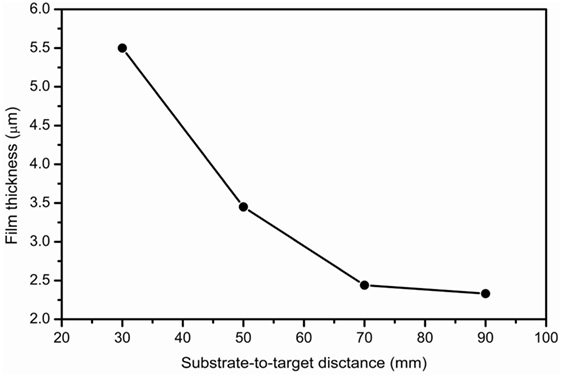
Figure 1. Variation of film thickness as a function of target-to-substrate distance for molybdenum thin films deposited by DC-magnetron sputtering.
X-Ray Diffraction Analysis
Figure 2 shows the low angle XRD pattern for Mo films deposited using DC-magnetron sputtering at various target-to-substrate distances. Films deposited on corning glass were used for the XRD measurement. It is evident from the figure that all films show two distinct peaks at 2θ ~40.5° and 73.7° corresponding to (110) and (211) crystal orientations, respectively. As seen the intensity of (110) diffraction peak monotonically increases with increase in target-to-substrate distance and at the same time the intensity of (211) diffraction peak decreases with increase in target-to-substrate distance. Thus, at low target-to-substrate distances (<50 mm) Molybdenum films have preferred orientation of crystallites in (211) direction and the films deposited at higher target-to-substrate distance (>50 mm) Mo films have preferred orientation in (110) direction. Therefore, XRD analysis revealed that with increase in target-to-substrate distance the preferred orientation of Mo crystallites changes from (211) to (110). The change in preferred orientation of Mo crystallites may be due to the competition between the stain energy and surface energy of the growing film which affects the texture of the grain (Checchetto, 1997; Jeyachandran et al., 2007). We think that due to low surface energy at lower target-to-substrate distance the (211) plane is the preferred orientation for the Mo films. However, with increase in target-to-substrate distance the intensity of (110) diffraction plane increases which may be due to stress activated mechanism during the film growth. The calculated lattice parameter was found in the range 3.14–3.15 Å over the entire range of target-to-substrate distance studied, which is consistent with the value of bulk Mo (3.15 Å).
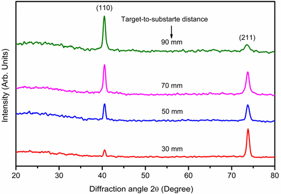
Figure 2. XRD pattern of molybdenum thin films deposited at different target-to-substrate distances by DC-Magnetron sputtering.
The average crystallite size calculation was performed using the Scherrer’s formula (Cullity and Stock, 2001),
where λ is the wavelength of the X-ray used, β is full-width at half-maximum (FWHM), and θβ is the Bragg diffraction angle. The calculated structural parameters are presented in Table 2. As seen from Table 2, the average crystallite size of Mo films decreases with increasing target-to-substrate distance.
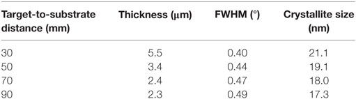
Table 2. Structural parameters, average crystallite size, full-width half maxima (FWHM), and thickness for molybdenum films prepared at different target-to-substrate distance.
FE-SEM Analysis
The microstructure of the deposited Mo thin films was observed with FE-SEM. Figure 3 shows FE-SEM images of Mo thin films deposited using DC-magnetron sputtering at various target-to-substrate distances. All FE-SEM images were acquired at 50,000× magnification. As seen the surface of all films are uniform and dense without defects such as cracks, pinholes, and protrusion. However, a significant change has been observed in surface morphology with increase in target-to-substrate distance. The Mo film deposited at 30 mm target-to-substrate distance exhibit irregular prismatic shape like morphology. With increase in target-to-substrate distance the density of prismatic grain increases; however, its size decreases (Figures 3B,C). We believe that at low target-to-substrate distance, due to Ar+ ions impingement, the Mo atoms ejected from the target tends to nucleate at the substrate surface with each other more easily to form larger prismatic grain size and the corresponding density is less. With increase in target-to-substrate distance the ejected Mo atoms have sufficient time in raising their surface energy before reaching the substrate surface. It results into decrease in prismatic grain size and increase in its density. Further increase in target-to-substrate distance to 90 mm, irregular prismatic shape morphology of Mo transform into closely packed uniform and smooth spherical grains (Figure 3D). Such smoother films formed at higher target-to-substrate distance can be useful for better adhesion of buffer layer in CZTS solar cells.
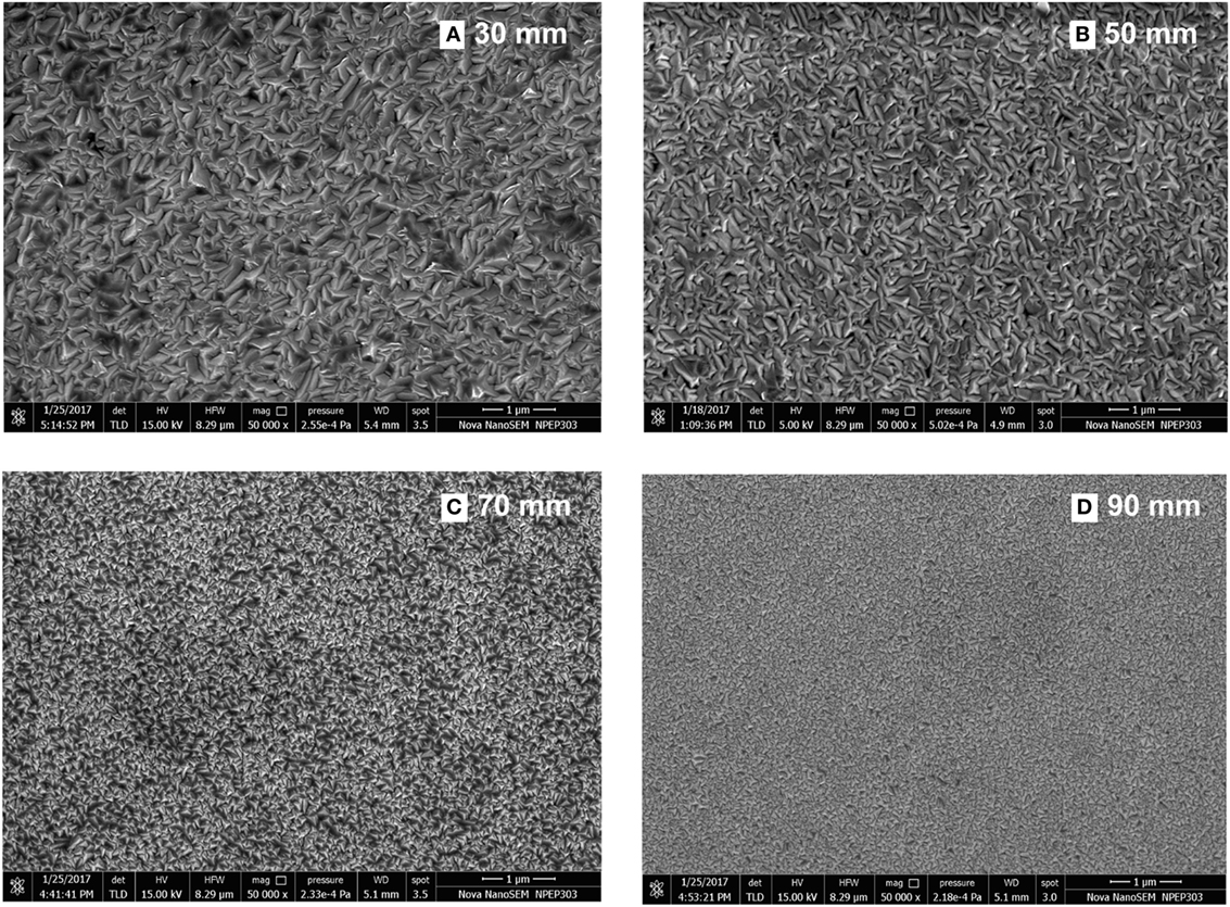
Figure 3. Field emission scanning electron microscope images of the molybdenum thin films deposited by DC-magnetron sputtering at various target-to-substrate distance (A) 30, (B) 50, (C) 70, and (D) 90 mm.
UV-Visible Spectroscopy Analysis
Reflection from back metal contact is an important in view of improving the CZTS solar cell efficiency. By maximizing the reflectance from the back metal contact, multiple photons can be absorbed in the absorber layer of CZTS solar cells which results an increase in its efficiency. Figure 4 shows the UV-Visible reflection spectra of Mo thin films deposited by DC-magnetron sputtering at different target-to-substrate distances. As seen from the figure Mo films deposited at higher target-to-substrate distance have better reflection than those deposited at lower target-to-substrate. These results suggest that Mo films deposited at higher target-to-substrate distances are more suitable for CZTS solar cells.
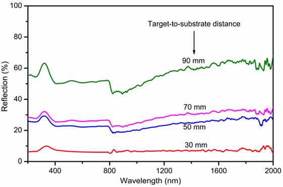
Figure 4. Reflectance of molybdenum thin films deposited at various target-to-substrate distance by DC-magnetron sputtering.
Electrical Properties
The Van der Pauw method has been used to measure the sheet resistance and electrical resistivity of the deposited Mo thin films. The sheet resistance of Mo thin films increase from 0.3 to 1.0 Ω/sq when target-to-substrate distances increased from 30 to 90 mm. Figure 5 shows variation of resistivity of Mo thin films deposited by DC-magnetron sputtering at different target-to-substrate distances. As seen that the resistivity of Mo thin films increases almost linearly with increase in target-to-substrate distance. It increases from 0.8 × 10⁻⁵ to 8.3 × 10⁻⁵ Ω·cm as the target-to-substrate distance increased from 30 to 90 mm. The values of resistivity lies within the range of values reported by Scofield et al. (1995) and Yoon et al. (2004) for Mo films deposited on soda-lime glass substrates using a DC-magnetron sputtering system. Increase in resistivity can attributed to decrease in average grain size and increase in grain density with increase in target-to-substrate distance. Increase in grain density increases grain boundaries. This increases grain boundary potential barrier height during electrical transport and it leads to hinder the carrier mobility. As a result, the resistivity Mo thin film increases with increase in target-to-substrate distance. The increase film thickness also leads to the increase in resistivity of Mo films (Gordillo et al., 2006).
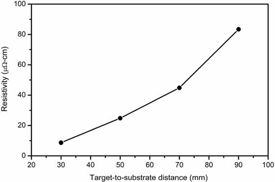
Figure 5. Variation of resistivity of molybdenum thin films deposited at various target-to-substrate distance by DC-magnetron sputtering.
Adhesion of Mo Thin Films
The adhesion of the films was investigated with scotch tape adhesion test by gluing the tape on the surface of Mo films and it by applying manual force. No delamination of Mo films from the substrate was observed suggesting that the as-deposited Mo films deposited on glass substrate have excellent adhesion property.
Conclusion
In conclusion, thin films of Mo were prepared by DC-magnetron sputtering by varying the target-to-substrate distance. These films were characterized for structural, optical, electrical, and morphological properties. It is observed that with increase in target-to-substrate distance the thickness of Mo films decreases. The XRD analysis revealed that with increase in target-to-substrate distance the preferred orientation of Mo crystallites changes from (211) to (110). Furthermore, the average crystallite size decreases with increase in target-to-substrate distance. Surface morphology studied using FE-SEM showed that all films are uniform and dense without defects such as cracks, pinholes, and protrusion. It has been observed that Mo film deposited at 30 mm of target-to-substrate distance exhibit irregular prismatic shape like morphology. However, with increase in target-to-substrate distance the surface morphology transforms into closely packed uniform and smooth spherical grains. The electrical properties investigated using van der Pauw method showed that the resistivity of Mo thin films increases linearly with increase in target-to-substrate distance. No delamination of Mo films from the substrate was observed suggesting that films have excellent adhesion property. We believed that employment of such Mo thin films as back contact in CZTS solar cells can improve its power conversion efficiency.
Author Contributions
All authors contributed equally to this work.
Conflict of Interest Statement
The authors declare that the research was conducted in the absence of any commercial or financial relationships that could be construed as a potential conflict of interest.
References
AbouElfotouh, F. A., Kazmerski, L. L., Coutts, T. J., Matson, R. J., Asher, S. E., Nelson, A. J., et al. (1989). Interface properties of (Cd,Zn)S/CuInSe2 singlecrystal solar cells. J. Vac. Sci. Technol. A7, 837–841. doi: 10.1116/1.575851
Abou-Elfotouh, F. A., Kazmerski, L. L., Matson, R. J., Dunlavy, D. J., and Coutts, T. J. (1990). Studies of the electrical and interface properties of the metal contacts to CuInSe2 songle crystals. J. Vac. Sci. Technol. A8, 3251–3254. doi:10.1116/1.576573
Ashour, S., Alkuhaimi, S., Moutinho, H., Matson, R., and Abou-Elfotouh, F. (1993). Junction formation and characteristics of CdS/CuInSe2/metal interfaces. Thin Solid Film 226, 129–134. doi:10.1016/0040-6090(93)90217-D
Checchetto, R. (1997). Titanium thin film deposition in a deuterium atmosphere. Thin Solid Films 302, 77–83. doi:10.1016/S0040-6090(96)09552-1
Gordillo, G., Mesa, F., and Calderon, C. (2006). Electrical and morphological properties of low resistivity Mo thin films prepared by magnetron sputtering. Braz. J. Phys. V36/3B, 982–985. doi:10.1590/S0103-97332006000600049
Green, M. A., Emery, K., Hishikawa, Y., Warta, W., Dunlop, E. D., Levi, D. H., et al. (2017). Solar cell efficiency tables (version 49). Prog. Photovolt. Res. Appl. 25, 3–13. doi:10.1002/pip.2855
Jeyachandran, Y. L., Karunagaran, B., Narayandass, S. K., and Mangalaraj, D. (2007). The effect of thickness on the properties of titanium films deposited by dc magnetron sputtering. Mater. Sci. Eng. A 458, 361–365. doi:10.1016/j.msea.2006.12.088
Jiang, F., Ikeda, S., Harada, T., and Matsumura, M. (2014). Pure sulfide Cu2ZnSnS4 thin film solar cells fabricated by preheating an electrodeposited metallic stack. Adv. Energy Mater. 4, 1301381. doi:10.1002/aenm.20130138
Katagiri, H., Jimbo, K., Shwe Maw, W., Oishi, K., Yamazaki, M., Araki, H., et al. (2009). Development of CZTS-based thin film solar cells. Thin Solid Films 517, 2455–2460. doi:10.1016/j.tsf.2008.11.002
Matson, R. J., Jamjoum, O., Buonaquisti, A. D., Russell, P. E., Kazmerski, L. L., Sheldon, P., et al. (1984). Metal contacts to CuInSe2. Solar Cells 11, 301–305. doi:10.1016/0379-6787(84)90019-X
Moons, E., Engelhard, T., and Cahen, D. (1993). Ohmic contacts to p-CuInSe2. J. Electron. Mater. 2, 275–280. doi:10.1007/BF02661377
Muhunthan, N., Singh, O. P., Thakur, M. K., Karthikeyan, P., Singh, D., Saravanan, M., et al. (2014). Interfacial properties of CZTS thin film solar cell. J. Solar Energy 2014, ArticleID476123. doi:10.1155/2014/476123
Niles, D. W., Nelson, A. J., Schwerdtfeger, C. R., Hochst, H., and Rioux, D. A. (1992). A photoemission investigation of the interfacial electronic properties of Mo and Ni schottky barrier to CuInSe2 (112). Mater. Res. Soc. Symp. Proc. 260, 299–304. doi:10.1557/PROC-260-299
Scofield, J. H., Duda, A., Albin, D., Ballardb, B. L., and Predeckib, P. K. (1995). Sputtered molybdenum bilayer back contact for copper indium diselenide-based polycrystalline thin-film solar cells. Thin Solid Films 260, 26–31. doi:10.1016/0040-6090(94)06462-8
Takedaa, S., Suzukia, S., Odakaa, H., and Hosono, H. (2001). Photocatalytic TiO2 thin film deposited onto glass by DC magnetron sputtering. Thin Solid Films 392, 338–344. doi:10.1016/S0040-6090(01)01054-9
Todorov, T. K., Reuter, K. B., and Mitzi, D. B. (2010). High-efficiency solar cell with earth-abundant liquid-processed absorber. Adv. Energy Mater. 22, E156–E159. doi:10.1002/adma.200904155
Keywords: Mo thin films, DC sputtering, XRD, field emission scanning electron microscope, UV-visible spectroscopy
Citation: Pandharkar SM, Rondiya SR, Rokade AV, Gabhale BB, Pathan HM and Jadkar SR (2018) Synthesis and Characterization of Molybdenum Back Contact Using Direct Current-Magnetron Sputtering for Thin Film Solar Cells. Front. Mater. 5:13. doi: 10.3389/fmats.2018.00013
Received: 06 July 2017; Accepted: 22 February 2018;
Published: 23 March 2018
Edited by:
Sravendra Rana, University of Petroleum and Energy Studies, IndiaReviewed by:
Nanda Gopal Sahoo, Kumaun University, IndiaPrabhakar Rai, Indian Institute of Technology Kanpur, India
Copyright: © 2018 Pandharkar, Rondiya, Rokade, Gabhale, Pathan and Jadkar. This is an open-access article distributed under the terms of the Creative Commons Attribution License (CC BY). The use, distribution or reproduction in other forums is permitted, provided the original author(s) and the copyright owner are credited and that the original publication in this journal is cited, in accordance with accepted academic practice. No use, distribution or reproduction is permitted which does not comply with these terms.
*Correspondence: Sandesh R. Jadkar, sandesh@physics.unipune.ac.in