 Farida Veliev1
 Anne Briançon-Marjollet
 Vincent Bouchiat
 Cécile Delacour
- 1Institut Néel, Centre National de la Recherche Scientifique and Université Grenoble Alpes, Grenoble, France
- 2Grenoble Alpes, HP2 Laboratory, Institut National de la Santé et de la Recherche Médicale U1042, Grenoble, France
The emergence of nanoelectronics applied to neural interfaces has started few decades ago, and aims to provide new tools for replacing or restoring disabled functions of the nervous systems as well as further understanding the evolution of such complex organization. As the same time, graphene and other 2D materials have offered new possibilities for integrating micro and nano-devices on flexible, transparent, and biocompatible substrates, promising for bio and neuro-electronics. In addition to many bio-suitable features of graphene interface, such as, chemical inertness and anti-corrosive properties, its optical transparency enables multimodal approach of neuronal based systems, the electrical layer being compatible with additional microfluidics and optical manipulation ports. The convergence of these fields will provide a next generation of neural interfaces for the reliable detection of single spike and record with high fidelity activity patterns of neural networks. Here, we report on the fabrication of graphene field effect transistors (G-FETs) on various substrates (silicon, sapphire, glass coverslips, and polyimide deposited onto Si/SiO2 substrates), exhibiting high sensitivity (4 mS/V, close to the Dirac point at VLG < VD) and low noise level (10−22 A2/Hz, at VLG = 0 V). We demonstrate the in vitro detection of the spontaneous activity of hippocampal neurons in-situ-grown on top of the graphene sensors during several weeks in a millimeter size PDMS fluidics chamber (8 mm wide). These results provide an advance toward the realization of biocompatible devices for reliable and high spatio-temporal sensing of neuronal activity for both in vitro and in vivo applications.
Introduction
The current non-invasive technologies (for instance functional MRI, EEG) enable the real-time monitoring of the whole brain activity. Those techniques have already provided impressive mapping of neuronal architectures in-situ (Zupanc, 2017). However, these far-field approaches integrate signals of a large population of cells (volume around mm3) and are far below single-cell resolution. For neuro-rehabilitation process, one needs to stimulate, detect, and track the activity of specific single neurons, as shown for restoring accurate motor motion (Hochberg et al., 2012; van den Brand et al., 2012) sensory feedbacks (Raspopovic et al., 2014) or vision (Hornig et al., 2005). To get a closer access to single cells and sub-cellular nanoscale events, optical techniques could be used for instance to manipulate ion channel activity (Szobota and Isacoff, 2010), to follow sub-threshold electrical signals along neuronal arborization (Zecevic, 1996; Tanese et al., 2017) or to track neurotransmitters release (Nicovich et al., 2017). Also, electronics devices can provide quantitative information and are still required for long lasting recordings or when interfacing unaltered (genetically or stained) cells.
The current devices which are widely used since the 1980's for detecting the electrical activity of brain cells consist of microelectrodes arrays (MEA) (Thomas et al., 1972; Spira and Hai, 2013). They form capacitive systems with the surrounding cells and tissues, which can sense small variations of local field potential or even spikes, and can also stimulate the cells electrical activity thanks to their high interfacial impedance. Already used a few centuries ago by Galvani for stimulating frogs muscles, the reduction of the electrodes size has started with the emergence of microelectronics. Today, they allow accurate mapping of neural network activity with single cell resolution (Huys et al., 2012; Bakkum et al., 2013; Müller et al., 2015). The fabrication process, the electronics, and the spike sorting analysis are now well advanced and the technology is commercially available. Also, several materials have been tested so far, such as, diamond (Piret et al., 2015), platinium (Oka et al., 1999), gold (Brüggemann et al., 2011), carbon nanotubes (Keefer et al., 2008; Suzuki et al., 2013), and vertical nanowires (Robinson et al., 2012). However, there is still an interest in new devices and materials. The main drawback of microelectrodes is the size issue. The electrode probing area cannot be reduced while keeping high signal-to-noise ratio. Indeed, the detection being based on charges injection, the current response is inversely proportional to the electrode/electrolyte impedance. Therefore, a reduction of the electrode surface results in an increased impedance and reduced signal-to-noise ratio.
In order to detect low transient changes of extracellular potential associated to neural spikes (~10 μV), the electrodes areas S need to be typically around 2–50 μm in diameter and thus are much larger than single neurons (around 1 and 10 μm for neurite and soma). Today, even the smallest MEAs cannot provide access to single neurites, synapses, and ion channels (Spira and Hai, 2013). However, this activity at or below the single cell limit is involved in numerous brain processes such as, plasticity (Ribrault et al., 2011) and channelopathies (Ashcroft, 2006) or neurodegenerative diseases. Also, monitoring the propagation of single spikes along neural architectures could be crucial for cells biology, pharmaceutics, and medical healthcare. For that purpose, higher spatio-temporal resolutions are required as well as reliable and long lasting devices.
Since few years, field effect transistors (FETs) have attracted particular attention. Based on a modulation of the charge carrier density as function of the surrounding electrical field, the FET sensitivity is proportional to the width-to-length aspect ratio W/L of the transistor channel instead of its surface: (RSze et al., 1981)
with gm the FET transconductance, IDS and VDS the drain source current and voltage, VLG the gate voltage, μ the charge carriers mobility, CEDL the interfacial capacitance. Thus, the device size can in principle be downscaled way below the single cell limit while still keeping significant sensitivity, allowing spikes tracking along neurites and neural networks (Hutzler et al., 2006; Patolsky et al., 2006) and the detection of microscopic events such as, neurotransmitters release (Wang et al., 2007), DNA bases (Kim et al., 2004), or proteins recognition (Chen et al., 2011).
Meanwhile, graphene has emerged as promising 2D platform for bio- and neuro-electronics (Schmidt, 2012; Kostarelos et al., 2014) regarding the high chemical stability and biocompatibility of the sp2-hybridized carbon lattice. Moreover, the higher charge carriers motilities and the absence of top gate oxide have allowed to overcome the threshold performance of the semiconductors technology with higher transconductance and devices sensitivity (S = 4.23 mS/V for G-FET vs. 0.2 mS/V for silicon FET; Hess et al., 2011a).
Large sheets of polycrystalline monolayered graphene can be grown by chemical vapor deposition on copper foils and further transferred on a wide range of substrates at the manufacturing level (Bae et al., 2010) allowing large-scale integration of the devices on transparent, soft, and flexible substrates suitable for real time optical stimulation or imaging of the interfaced cells. Also, the mechanical properties of graphene allow the implementation of stretchable—and still highly conductive—electronics for matching the non-planar geometry of cells and keeping an intimate contact. Together with its flexibility, its possible implementation on soft substrates could reduce the inflammatory response of the body which currently prevents reliable and long lasting neural interfaces in vivo (Kuzum et al., 2014; Jeong et al., 2015).
Moreover, the positive impact of graphene on cells regrowth and maturation have been shown in numerous studies including primary neurons (Bendali et al., 2013; Veliev et al., 2016) and stem cells (Park et al., 2011) without altering their electrical activity (Fabbro et al., 2016). The cytocompatibility is certainly one of the main advantages of graphene in comparison with other 2D materials. The high adhesion on pristine graphene (without any additional adhesive coating) provides also high sealing with neurons, a feature which is a key parameter for extracellular measurement, while the fast regrowth of neurites could promote the regeneration of the damaged neural network when interfacing native tissues or dissociated cells in culture. Also, the small amount of implanted materials is an advantage to reduce the toxicity risks. Indeed, several studies have shown that macrophages degrade efficiently graphene flakes when introduced in several organs of the body (Bianco, 2013; Girish et al., 2013).
Since the past few years, graphene field effect transistors (G-FETs) have been able to provide versatile detectors that enabled to sense low pH change (Ohno et al., 2009) DNA translocation (Xu et al., 2017) cancer cells (Feng et al., 2011), or bacteria (Mannoor et al., 2012). Also, G-FETs were able to detect single spike evoked in electrogenic cells line, such as, cardiomyocytes (Cohen-Karni et al., 2010) or HEK/PC12 cells (Hess et al., 2011b) and more recently ion channel activity (Veliev et al., 2017) and slow potential waves resulting from synchronous activity of a large population of neurons have been recorded by electrocorticograms performed on living rats (Blaschke et al., 2017). Compared to previous results, one has to note that neurons are much smaller, fragile, and less accessible. However, these results hint the possibility to record single spike from single neurons with an implantable graphene based bioelectronics.
Here, we report on the fabrication of G-FETs arrays on transparent and flexible substrates (sapphire, glass, coverslip, and polyimide substrates, still compared with conventional silicon on insulator substrates) and their ability to record the spontaneous activity of primary hippocampal neurons cultured in-situ, on the chip, in a microfluidic chamber, during 21 days until the maturation of the network was complete.
Results and Discussions
Graphene monolayers are grown by chemical vapor deposition on 25 μm thick copper foils (99.8% purity, Alfa-Aesar) by decomposition of methane gas CH4 at 1,000°C in diluted hydrogen atmosphere as previously described (Han et al., 2014). After cleaning in acetone, the cooper foils is annealed in diluted H2 atmosphere (dilution in Ar at 10%) at 1,000°C for 2 h to reduce the native copper oxide and enlarge the copper grains. Then, pulses of methane CH4 (2 sccm 10 s, then 60 s off) are injected as a carbon source, instead of using continuous flow of methane, to prevent the aggregation of carbon at the nucleation centers and avoid the formation of multi-layers patches. This pulse growth enables to reach higher carriers mobilities values up to 6,700 cm2/V/s (Han, 2013).
Pieces of Cu foil of about 4 × 4 mm2 with graphene monolayers on top, are then transferred on the substrates—Si/SiO2, sapphire, glass coverslip (Marienfeld), and polyimide (deposited on Si/SiO2 substrates)—by wet transfer technique. Briefly, a plastic carrier (spin-coated PMMA film) is deposited on top of the graphene layer, then the copper foils is etched in solution containing specific Cu etchant [(NH4)2S2O8 at 0.1 g/ml]. Once the Cu foil is completely dissolved, the bilayer (Graphene-PMMA) is rinsed three times in deionized (DI) water to remove the etchant and is then wet-transferred onto the host substrate. The PMMA resist is removed in acetone (overnight bath), then the sample is rinsed and annealed at 300°C for 3 h in diluted hydrogen atmosphere (H2/Ar, mbar) to remove PMMA residues. Optical and atomic force micrographs (Figures 1a,b, respectively) show the overall continuity and homogeneity of the transferred graphene monolayer and the quasi absence of PMMA residues. Micro-Raman spectra assess for the crystalline quality of the transferred graphene monolayer. Each trace represents the averaged value of several measurements performed at different points around the channel. Figure 1c shows the two main Raman lines of graphene, the G-mode (1,580 cm−1), and 2D-mode (2,700 cm−1). Their widths w2D = 24 cm–1 and intensity ratio I2D/IG = 0.3 are as expected for single graphene layer (Ferrari and Basko, 2013). The absence of the D-peak (expected around 1,350 cm–1) confirms the high quality of the monolayer.
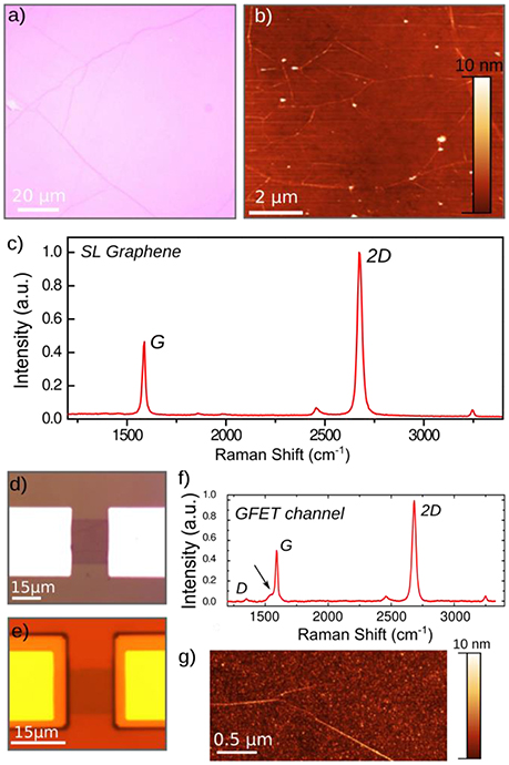
Figure 1. Surface and structural characterizations of the CVD-grown graphene monolayers. (a) Optical micrograph of a typical graphene monolayer grown by pulsed CVD, after transfer on oxidized silicon (285 nm SiO2). (b) Atomic force micrograph of the graphene surface after transfer and annealing at 300°C for 3 h. (c) Raman spectroscopy underlying the characteristic Raman peaks of graphene monolayers (detailed in the text). Optical images of the graphene channel (20 × 15 μm2) before (d) and after (e) passivation. (f) Raman spectrum of the active graphene FET channel of the final device after contact passivation by photoresist. (g) Atomic force micrograph of the graphene FET channel after passivation.
The transistors arrays are micro-fabricated by first etching the graphene in stripes that will act as transistor channels. This is done by patterning channels with a photoresist mask and etching of the unprotected parts using oxygen plasma. Contact leads are then deposited using a photoresist mask and evaporation in vacuum of metal thin films (Ti/Pt/Au or Pd). Pd was used as the metal contact on sapphire substrates, while Ti/Pt/Au was rather used on PID and glass coverslips to enhance the adhesion of the metal onto the substrates. For SiO2 substrates, we have used both Pd and Ti/Pt/Au (for comparison with the sapphire, and the glass or PID substrates, respectively). The contact resistance is qualitatively estimated by measuring the two-point resistance of G-FETs with different widths, being around RC = 0.3 kΩ, per contact, while the square resistance R□ of the graphene sheet is about R□ = 0.65 ± 0.05 kΩ/□ (Veliev et al., 2017). Finally, the metallic contact leads are insulated using biocompatible polymers, either polyimide (Fujifilm, photosensitive PID) or the negative photoresist SU8-2000, and are annealed during 2 h at 200°C in N2 atmosphere, and 30 min at 150°C, respectively. No significant difference was observed on the GFETs performances. However, the SU8 provides a lower fluorescent background noise for the immuno-fluorescent stainings used to locate the cells after the recordings. Smallest G-FETs arrays with channel width and length of W × L = 20 × 15 μm2 were realized (Figure 1d). The effective gate length (graphene area exposed to the liquid gate) is reduced to 10 μm after passivation of the metal contact leads, regarding the overlaps between the graphene channel and the passivation layer (Figure 1e). Optical micrographs of the graphene FET channel show the absence of large contaminant after deposition (Figure 1d) and passivation (Figure 1e) of the metal contacts. For some devices, a common ground electrodes were designed to increase the number of GFETs (80 per chips), as shown in Figure 4 for instance.
To detect a possible degradation of the crystalline quality of graphene by the FET fabrication process, Raman is performed after process (Figure 1f). The integral intensity ratio IG /I2D = 0.33 of the G and 2D mode peaks, as well as the width of the 2D peak ω2D = 31 cm–1 and the low intensity of the defect-induced D-peak, reveal the high quality of graphene even after the FETs fabrication. A new peak appears on the right shoulder of the G-peak however, which could indicate the presence of resist residuals. Atomic force micrographs reveal indeed a slight (nanometer scale) contamination of the surface (Figure 1g).
The sensitivity of the fabricated G-FETs is measured with a liquid top gate, with either cell culture medium or PBS solution, and biased with a Pt or Ag/AgCl reference electrodes. Either Pt or Ag/AgCl reference electrode could be used as a gate electrode, as both gate electrodes showed identical transconductance. Due to the high capacitance of the electrical double layer at the graphene/liquid interface (CEDL ~2 μF/cm2), a low variation of the liquid gate potential could induce a high modulation of the drain-source current IDS through the transistor channel. By increasing the gate potential, the transistor operation mode varies from hole to electron conduction regime by passing the conductance minimum at the charge neutrality point (Dirac point), typically around VCNP ~ 0.4 V, depending on the substrates and the used reference electrodes. Figure 2a depicts the principle of the neuron-covered liquid-gated FET (top) and the electrical setup (bottom), while Figure 2b shows the reproducible field effect responses of the G-FETs gated with the liquid potential, showing the reliability of the fabrication process per chip.
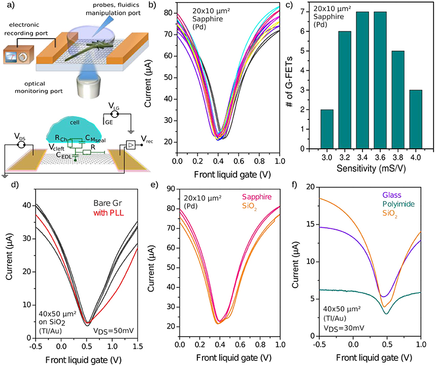
Figure 2. Performance of G-FETs arrays on several substrate. (a) Schematic view of an inverted microscope setup using transparent graphene electronics for simultaneous electrical and optical recording, cell control and fluidic manipulation. The electrical equivalent circuit of the graphene digital interface is described below. (b) Field effect characteristics of liquid-gated field effect measured on 10 devices showing reproducible behavior and narrow distribution of parameters. The measurements were performed on 20 × 10 μm2 G-FETs fabricated on sapphire at VDS = 75 mV with Pd/Au metallic contacts. (c) Sensitivity distribution of 30 identical FETs on the same chip than (b). (d) Field effect characteristics of liquid-gated G-FETs (40 × 50 μm2) on SiO2 before and after covering with poly-L-lysine (PLL). (e) Comparison of liquid-gated G-FETs (20 × 10 μm2) fabricated on SiO2/Si and on sapphire substrates (VDS = 75 mV, Pd metallic contacts) and (f) the G-FETs (40 × 50 μm2) fabricated on SiO2/Si, Glass and PID substrates (VDS = 30 mV, Ti/Pt/Au metallic contacts). All measurements were performed in cell culture medium using Pt reference electrode.
The sensitivity of the G-FET is proportional to the G-FET transconductance—defined as the differential conductance gm = ∂IDS/∂VLG—normalized by the bias drain-source voltage such as, S = gm /VDS. The mean value of the G-FETs sensitivity is around S = 3.5 mS/V, and maximal values reaches 4 mS/V for the 20 × 10 μm2 G-FETs on sapphire substrate (Figure 2c). These values are comparable with the highest reported G-FET performance for CVD grown graphene(Hess et al., 2011a).
Coating the sample with a capping layer that promotes cell adhesion is widely used to ensure high attachment and neurites regrowth onto the samples, especially for primary neurons which require weeks of culture for establishing a mature (electrically connected) network. Synthetic polymers such as, poly-L-lysin are generally used to bond the neurons membranes by taking advantage of electrostatic interactions. However, as these polymers are intercalated between graphene and neurons, they form a charged layer that affects carriers mobility within the graphene channel and thus lead to decrease signal-to-noise ratio by partially screening the neuron gating signal. Indeed, after functionalization, the conductance Vs Gate curve shows a slightly broadened dip and exhibits two local minima, suggesting the presence of fluctuations of doping levels in graphene (Figure 2d). However, the transconductance on both hole and electron sides is barely affected by the coating, as expected for a non-covalent PLL/Graphene interactions (Wang et al., 2013) and thus the G-FET sensitivity remains the same with and without the PLL coating, at least in the highest sensitive operating points.
A main advantage of graphene and 2D materials is the possibility to integrate them on transparent and flexible substrates allowing a see-through operation compatible with optical microscope or microfibers in vivo (see Figure 2a). Figures 2e,f compare the transconductance (IDS-VLG curves) of the G-FETs supported on diverse materials such as, glass coverslips, sapphire, and polyimide in comparison with conventional Si/SiO2 substrates. While the electrical characteristics of G-FETs fabricated on glass coverslip and Si/SiO2 are almost identical—the square-normalized sensitivity S = S□ × L/W being 1.2 mS.V−1.□ and 1.36 mS. V−1.□ for glass coverslip and Si/SiO2, respectively—the devices realized on polyimide exhibit higher contact resistance and a slightly shifted Dirac point toward higher doping level (with S□ = 0.8 mS.V−1.□). Nevertheless, the extracted transconductance values are almost similar for all substrates, indicating that one performance limitation of G-FETs fabricated on glass or soft PID substrates could be the higher contact resistance. The devices fabricated on sapphire show highest sensitivity value (S□ = 8 mS.V−1.□) which could result from a lower density of charges trapped at the interface with the substrate. This performance is one of the highest reported for CVD grown grapheme (Hess et al., 2011a). We tested the ability of the GFETs to detect potential pulses with shape and amplitude similar to the expected extracellular neuronal spike. At the operation point (the highest operating regime, underlined with the blue star Figure 3a), GFETs enable the detection of short pulses (1 ms) of low amplitude (75 μV) applied to the cell culture medium through a Pt-electrode (Figure 3b). The power spectral noise density of the G-FETs in two-points measurement configuration shows a dependence in frequency according to 1/f law for the low frequency regime with a noise level around 10−22 A2/Hz at 1 kHz (Figure 3c). This low noise level is expected for graphene in comparison to silicon, and could be in part explained by the absence of top gate oxide which acts as an additional source of noise in semiconductors devices (Balandin, 2013). This density or mobility fluctuations within the FET channel could result either from charge traps at the interface with the substrates, or from defects at the edges of the graphene channels that can contribute to the Generation-Recombinaison G-R noise (Rumyantsev et al., 2010).
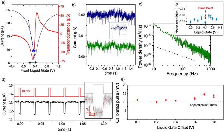
Figure 3. Noise and stability of the G-FETs for potential pulse detection. (a) Field effect and transconductance of the G-FETs measured in the cell culture medium. Dashed blue line indicates the linear operation regime of the G-FET with the maximal sensitivity. The black arrows highlight the gate voltage range of the maximal sensitivity around VLG = 0.3 V. The blue star indicates the operating point for the pulses detection shown in (b). (b) Detection of 100 μV (blue) and 75 μV (green) potential pulses (applied to the cell culture medium through a Pt-electrode) by G-FETs biased at VDS = 50 mV and VLG = 0.32 V. Inset: zoomed of the superimposed G-FETs responses. Scale bars are 2.5 nA and 10 ms (c) Power spectral density of the current noise in liquid gated G-FETs (VLG = 0 V). A 1/f dependence on the frequency is observed (dashed line). Inset shows the noise amplitude as function of the liquid gate voltage. (d) G-FET response (black line) to square shaped potential pulses (red line) applied in cell culture medium. Inset: zoom of a pulse detected by G-FET (blackline), revealing a very fast response (~0.5 ms) to the applied square pulse signal (redline). Gray line is the unfiltered signal. (e) Calibrated pulse height from GFET transconductance (a) of the potential pulse VP = 10 mV showing that the calibrated pulse and the applied pulse are in very good agreement.
The G-FETs provide a fast response time (at least faster than spike duration), with a rise time of τ ~ 0.5 ms (Figure 3d) and reliable detection of potential spikes applied in the liquid gate (Figure 3e), the minimal amplitude being VP = 75 μV with a signal-to-noise ratio around S/N ~2.5 (Figure 3b), which should allow the extracellular detection of neuronal spikes. The detection performance may vary depending on the cell/device coupling area and fluctuation around the operating point, which could arise from many processes when interfacing cells, such as, molecules adsorption or local pH changes. This could be overcome by low contact resistance which increases the range of the linear and highest sensitive regime (underlined with the arrow Figure 3a).
Primary neurons were cultured (Veliev et al., 2016) above the sensors during 21 days until the maturation of the network was complete. Briefly, the hippocampi are extracted from E16 mouse embryo. Neurons are mechanically dissociated and seeded (6 104 cell/cm2) onto the sterilized samples in attachment promoting medium (MEM supplemented with 10% fetal bovin serum). Samples were previously coated with poly-L-lysin (at 100 μg/ml over night, then rinsed) to enhance the adhesion of neurons over the surface. After 2 h, the medium is replaced by a serum free and glial conditioned neurobasal supplemented with AraC (cytosine arabinoside, at 1 μM) to prevent the proliferation of glial cells which would form a barrier between the sensors and the neurons. Neurons can be observed on the transparent sapphire or glass samples with conventional optical microscope, and be compared with control glass coverslips (without devices) during the culture time. After the measurements, neurons are fixed in 4% paraformaldehyde and immuno-histologies assess precisely the cells position and shape above the sensors, by labeling the soma, the synapses and the micrometer size neurites and axons, with DAPI (4′,6-diamidino-2-phenylindole, at 1 μl/ml), and anti-Synapsin (2 μg/ml), anti-YL1/2 (1 μg/ml), and anti-Tau (2 μg/ml) primary antibodies, respectively (Figure 4a).
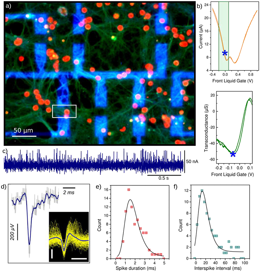
Figure 4. Primary hippocampal neurons interfaced with G-FETs (20 × 10 μm2). (a) Immuno-fluorescence micrographs of neurons on the G-FETs after 21 days of culture, stained with DAPI (red) and anti-Synapsin (green) to label the soma and the synaptic vesicles along the neuritis, respectively. The metal contact leads appear in blue and connect the graphene FET channel (the position of one G-FET is underlined with the white square for example). (b) G-FET current vs. liquid gate voltage, set using a Ag/AgCl reference electrode immersed into the cell culture medium (top) and corresponding transconductance curve (bottom) in the highest sensitive regime (underlined by the green square on the top curve). The blue star indicates the transistor working point with the highest sensitivity in the hole conduction regime. (c) Recording of neuronal activity by monitoring the ISD current of the G-FET underlined with a white square in (a), at the transistor working point indicated by a blue star in (b). The measurements were performed in cell culture medium (VSD = 100 mV). (d) The calibrated extracellular potential obtained from a single current spike, obtained from (c) and the transconductance value at the operating point (detailed in the text). The inset shows the superposition of all detected spikes. The scale bars are 200 μV and 2 ms. (e) Histograms showing the distribution of the spike duration and (f) distribution of the interspike interval (right).
The neuronal activity is monitored after 19–21 days of culture, in CO2 and temperature regulated atmosphere, using a needle probe station interfaced with FPGA electronics. The liquid gate voltage VLG is applied to a Pt or Ag/AgCl electrodes immersed into the solution. A constant DC drain-source bias voltage VDS is applied to the G-FET and the drain-source current through the transistor channel ISD is monitored using commercial and home made current amplifiers. To decrease the input noise, voltage dividers and low pass filters are used. The output signal is filtered using a low pass filter with a cut-off frequency fc = 5 kHz.
Immuno-fluorescent IF micrograph of neurons cultured on the G-FETs arrays is shown in Figure 4a, and the electrical properties of the interfaced G-FETs in Figure 4b. The recorded ISD traces exhibit short current pulses, which duration, amplitude and polarity are as expected for neuronal signals (Figure 4c). Using the transconductance gm at the set transistor operating point (underlined with the stars in Figure 4b), the extracellular potential can be estimated to Vextra = ISDgm. The calibrated extracellular potential is shown in Figure 4d. The amplitude is around 570 ± 80 μV, and the spike duration τ = 1.5 ± 0.1 ms (Figure 4e). The polarity and the shape of the detected signals correspond to the expected extracellular potential spike generated by the opening of sodium channels and influx of positively charged Na+ ions into the cell resulting in a negative potential change in the cleft and a positive variation of IDS. The signal amplitude seems high compared to values reported using MEAs (Spira and Hai, 2013) however for SiNW-FETs, extracellular action potentials with amplitude up to several mV were reported (Voelker and Fromherz, 2005). The interspike interval (ISI) Δt = 13 ± 0.8 ms (Figure 4f) is in good agreement with values reported for in vivo conditions (Chorev and Brecht, 2012) however slightly shorter than expected for in vitro neuronal cultures. But since the neuron density is high, it could be possible that the device (underlined with a white square Figure 4a) is recording action potentials originating from more than one neuron.
When the field effect curve is measured with live neurons on top of the FET devices (Figure 5a), a 0.2 V positive shift of the charge neutrality point can be observed along with a general conductance depression (Figure 5b). Also the field effect curve exhibits two local minima suggesting the coexistence of graphene with two well distinct doping. These observations can be clearly attributed to the presence of dense neuron networks adsorbed on the FETs surface, since after cleaning the device, the Dirac point shifts back to less positive gate voltage values, and the double conductance minimum almost disapears. A control experiement was performed without neuron, after 3 weeks of incubation in culture medium at 37°C (Figure S1). This shift of the Dirac point in presence of neurons can be attributed to the negative resting membrane potential (Figure 5a). Also, the excitability of neurons could slightly gates the GFET channel, the current being slightly lower when neurons activity is blocked (~95% of IDS, by adding tetrodotoxin at 0.5 μM in the cells medium) or when neurons are fixed (37% of IDS, after fixing neurons with 4% paraformaldehyde 10 min; Supplementary Figure S2).
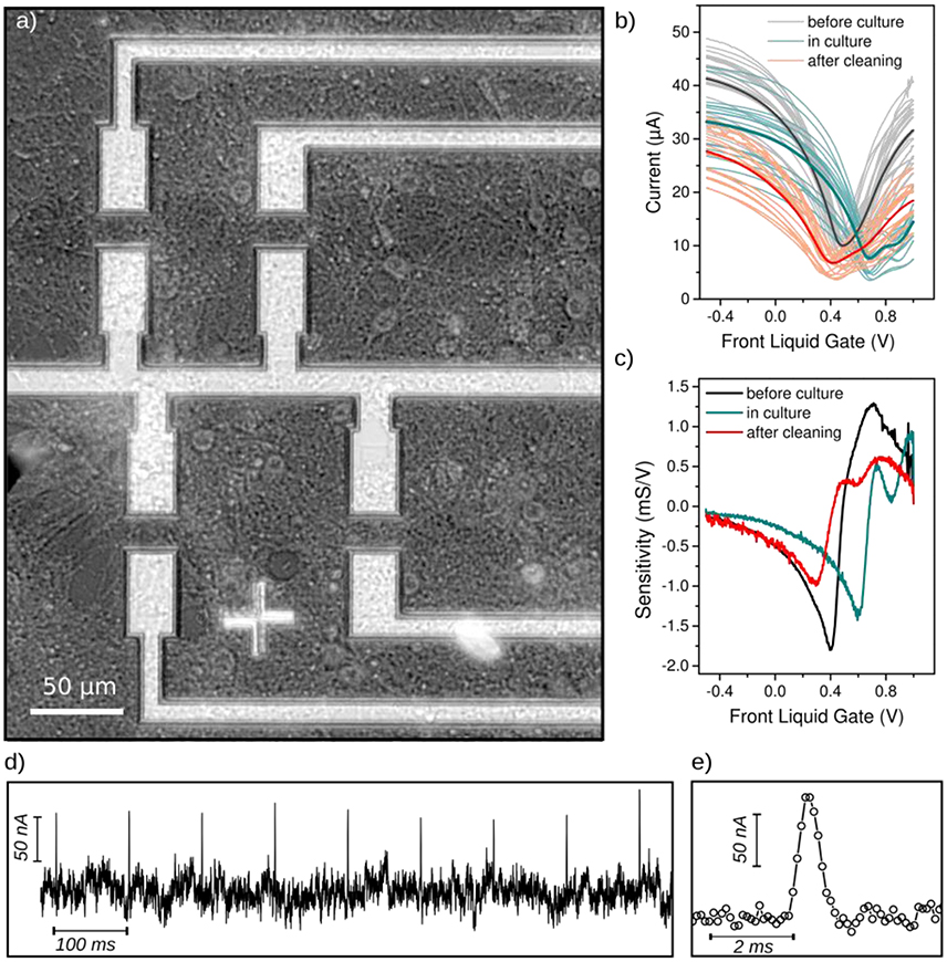
Figure 5. Performance of the G-FETs after 3 weeks of neurons culture. (a) Optical micrograph of the dense neuronal networks cultured on G-FETs during 21 days. (b) Field effect of liquid gated G-FETs before culture (gray curves), covered with 21DIV neurons (blue curves), and after cleaning the chip (orange curves). Curves represent one device, except the darker one which is the average field effect curves for each condition. All measurements were performed in cell culture medium at VSD = 50 mV. (c) Average sensitivity of G-FETs before the culture (black), covered with neurons (blue) and after cleaning (red). The sensitivity was calculated from the average field effect curves in (b). (d) Potential pulse detection using G-FETs covered with neurons. A 1 ms long potential pulse Vp = 500 μV was applied to the cell culture medium through a Pt-electrode; the transistor working point was set to the highest sensitivity, and the current through the FET-channel was measured at VSD = 100 mV. (e) Zoomed view of an individual current pulse detected in (d). A Pt-reference electrode was used as the gate electrode for all the measurements.
After the electrical recordings with neurons, the chip was immersed into warm DI water, resulting in the burst of neurons due to osmotic pressure. The chip was then rinsed several times with DI water and dried. After this simple cleaning procedure, the transfer characteristics of G-FETs were measured again in cell culture medium. After removing the neurons, the Dirac point shifted back to less positive voltage values (being closer to the value before the cell culture). However, the sensitivity of G-FETs was reduced to 50% of the initial value after the cleaning (Figure 5c). To re-use the chips for several cultures, the cleaning process has to be improved. First, DI water should not be used for removing the neurons, since the surface tension of water can lead to partial delamination of the graphene layer. For instance, a cleaning with an enzymatic bath (that does not damage the graphene monolayer) could be used to remove cellular matrix residuals. Also, characterizing the electrodes material with Raman microscopy could provide new insights on the structure of the graphene FETs channel after the cell culture.
The sensitivity of G-FETs is reduced by 25% during the culture (Figure 5c), which might be due to the damaged graphene surface induced by the tension of growing neurons and resulting in a lower mobility. On the other hand, the decreased sensitivity may arise from the reduced field effect due to the presence of a screening neuron layer on the FETs. Indeed, the FETs are still able to detect small potential changes such as, stimulated spike, as shown in Figure 5d, even with a reduced sensitivity. The positive and biphasic change of the drain source current (Figure 5e) strongly resembles the expected shape of evoked neuronal spike. A direct gating by the liquid should rather induce negative and monophasic variation of IDS such as, shown in Figure 3b without neurons.
This stable performance of G-FETs in the biological environment combined with the excitability of cultured neurons makes the detection of the neuronal activity and particularly single action potentials, using flexible and transparent G-FET feasible.
Nevertheless, further improvements of the devices performance should be investigated for reliable spike tracking and high detection efficiency, in term of number of spike detected per neurons and per devices. Electronics noise could be reduced using suspended graphene or by reducing the density of charges trapped at the interface with the substrate (Cheng et al., 2013). Also higher mobility could be obtained by increasing the crystalline quality of CVD grown graphene, for instance by enlarging the single grain size which should increase the sensitivity of the devices (Gao et al., 2012).
The use of 2D materials could be promising for bio-sensing applications and for interfacing neuronal networks in slices or in vivo nervous systems (CNS and PNS), regarding the possibility to combine a transparent digital interface with optical techniques (Kuzum et al., 2014). Also, the use of soft and flexible substrates could (be used to) reduce the inflammatory response and enable drugs delivery, to support the scarring process and the bioacceptance of the artificial interface (Minev et al., 2015; Lee et al., 2016). In addition with the chemical inertness and anti-corrosive properties of graphene, such bio-suitable features are crucial for implementing active scaffolds and long lasting neuronal interfaces in neurosciences and medicine.
Conclusion
The hippocampal neurons cultured on G-FETs exhibit healthy morphology and spontaneous electrical activity after 19–21 days in culture. The 1–2 h long electrical recordings performed on neurons using G-FETs do not damage the cells, at least no significant change is observed with immuno-fluorescent imaging of neurons after the measurements. Both shape and proteins expressions are as expected for 21 days old cultured neurons. The performance of G-FETs degrades slightly during the culture. However, the FETs are still able to detect small potential pulses on the range of action potential spikes generated by neurons. Both the neuron culturing technique used in this work and the FET performance are sufficient to pave the road for the realization of a cell-FET hybrid device and for recording electrical activity of single neurons with flexible and transparent substrates, useful for the large scale integration of suitable devices for bioelectronics and neuroprosthetics.
Author Contributions
FV, VB, and CD conceived and designed the project. FV and CD performed the devices and the neurons experiments. AB and CD performed the cells culture. ZH, DK, and VB performed the graphene growth. FV and CD analyzed the data and wrote the manuscript with VB and AB.
Conflict of Interest Statement
The authors declare that the research was conducted in the absence of any commercial or financial relationships that could be construed as a potential conflict of interest.
Acknowledgments
The authors thank the Hybrid, TPS and electronics teams for their support in materials, devices fabrication and electrical setup. Also the plateforms of nano and micro fabrication and cells culturing, Nano—and BioFab, respectively. The authors gratefully acknowledge financial support from la Région Rhône-Alpes (COOPERA project), and from the french Agence Nationale de la Recherche under the projects ANR-10-LABX-51-01 (Labex LANEF du Programme d'Investissements d'Avenir) the Lab Alliances on Nanosciences—Energies for the Future.
Supplementary Material
The Supplementary Material for this article can be found online at: http://journal.frontiersin.org/article/10.3389/fnins.2017.00466/full#supplementary-material
References
Bae, S., Kim, H., Lee, Y., Xu, X., Park, J.-S., Zheng, Y., et al. (2010). Roll-to-roll production of 30-inch graphene films for transparent electrodes. Nat. Nanotechnol. 5, 574–578. doi: 10.1038/nnano.2010.132
Bakkum, D. J., Frey, U., Radivojevic, M., Russell, T. L., Müller, J., Fiscella, M., et al. (2013). Tracking axonal action potential propagation on a high-density microelectrode array across hundreds of sites. Nat. Commun. 4, 218110. doi: 10.1038/ncomms3181
Balandin, A. A. (2013). Low-frequency 1/f noise in graphene devices. Nat. Nanotechnol. 8, 549–555. doi: 10.1038/nnano.2013.144
Bendali, A., Hess, L. H., Seifert, M., Forster, V., Stephan, A. F., Garrido, J. A., et al. (2013). Purified neurons can survive on peptide-free graphene layers. Adv. Healthc. Mater. 2, 929–933. doi: 10.1002/adhm.201200347
Bianco, A. (2013). Graphene: safe or toxic? The two faces of the medal. Angew. Chem. Int. Ed. 52, 4986–4997. doi: 10.1002/anie.201209099
Blaschke, B. M., Tort-Colet, N., Guimerà-Brunet, A., Weinert, J., Rousseau, L., Heimann, A., et al. (2017). Mapping brain activity with flexible graphene micro-transistors. 2D Mater. 4:025040. doi: 10.1088/2053-1583/aa5eff
Brüggemann, D., Wolfrum, B., Maybeck, V., Mourzina, Y., Jansen, M., and Offenhäusser, A. (2011). Nanostructured gold microelectrodes for extracellular recording from electrogenic cells. Nanotechnology 22:265104. doi: 10.1088/0957-4484/22/26/265104
Chen, K. I., Li, B. R., and Chen, Y. T. (2011). Silicon nanowire field-effect transistor-based biosensors for biomedical diagnosis and cellular recording investigation. Nano Today 6, 131–154. doi: 10.1016/j.nantod.2011.02.001
Cheng, Z., Hou, J., Zhou, Q., Li, T., Li, H., Yang, L., et al. (2013). Sensitivity limits and scaling of bioelectronic graphene transducers. Nano Lett. 13, 2902–2907. doi: 10.1021/nl401276n
Chorev, E., and Brecht, M. (2012). In vivo dual intra-and extracellular recordings suggest bidirectional coupling between CA1 pyramidal neurons. J. Neurophysiol. 108, 1584–1593. doi: 10.1152/jn.01115.2011
Cohen-Karni, T., Qing, Q., Li, Q., Fang, Y., and Lieber, C. M. (2010). Graphene and nanowire transistors for cellular interfaces and electrical recording. Nano Lett. 10:1098. doi: 10.1021/nl1002608
Fabbro, A., Scaini, D., León, V., Vázquez, E., Cellot, G., Privitera, G., et al. (2016). Graphene-based interfaces do not alter target nerve cells. ACS Nano 10, 615–623. doi: 10.1021/acsnano.5b05647
Feng, L., Chen, Y., Ren, J., and Qu, X. (2011). A graphene functionalized electrochemical aptasensor for selective label-free detection of cancer cells. Biomaterials 32, 2930–2937. doi: 10.1016/j.biomaterials.2011.01.002
Ferrari, A. C., and Basko, D. M. (2013). Raman spectroscopy as a versatile tool for studying the properties of graphene. Nat. Nanotechnol. 8, 235–246. doi: 10.1038/nnano.2013.46
Gao, L., Ren, W., Xu, H., Jin, L., Wang, Z., Ma, T., et al. (2012). Repeated growth and bubbling transfer of graphene with millimetre-size single-crystal grains using platinum. Nat. Commun. 3:699. doi: 10.1038/ncomms1702
Girish, C. M., Sasidharan, A., Gowd, G. S., Nair, S., and Koyakutty, M. (2013). Confocal raman imaging study showing macrophage mediated biodegradation of graphene in vivo. Adv. Healthc. Mater. 2, 1489–1500. doi: 10.1002/adhm.201200489
Han, Z. (2013). Macroscopic CVD Graphene for Nnanoelectronic: from Growth to Proximity Induced 2D Superconductivity. Doctoral dissertation, CNRS.
Han, Z., Kimouche, A., Kalita, D., Allain, A., Arjmandi-Tash, H., Reserbat-Plantey, A., et al. (2014). Homogeneous optical and electronic properties of graphene due to the suppression of multilayer patches during CVD on copper foils. Adv. Funct. Mater. 24, 964–970. doi: 10.1002/adfm.201301732
Hess, L. H., Hauf, M. V., Seifert, M., Speck, F., Seyller, T., Stutzmann, M., et al. (2011a). High-transconductance graphene solution-gated field effect transistors. Appl. Phys. Lett. 99:033503. doi: 10.1063/1.3614445
Hess, L. H., Jansen, M., Maybeck, V., Hauf, M. V., Seifert, M., Stutzmann, M., et al. (2011b). Graphene transistor arrays for recording action potentials from electrogenic cells. Adv. Mater. 23, 5045–5049. doi: 10.1002/adma.201102990
Hochberg, L. R., Bacher, D., Jarosiewicz, B., Masse, N. Y., Simeral, J. D., Vogel, J., et al. (2012). Reach and grasp by people with tetraplegia using a neurally controlledrobotic arm. Nature 485, 372–375. doi: 10.1038/nature11076
Hornig, R., Laube, T., Walter, P., Velikay-Parel, M., Bornfeld, N., Feucht, M., et al. (2005). A method and technical equipment for an acute human trial to evaluate retinal implant technology. J. Neural Eng. 2:S129. doi: 10.1088/1741-2560/2/1/014
Hutzler, M., Lambacher, A., Eversmann, B., Jenkner, M., Thewes, R., and Fromherz, P. (2006). High-resolution multitransistor array recording of electrical field potentials in cultured brain slices. J. Neurophysiol. 96, 1638–1645. doi: 10.1152/jn.00347.2006
Huys, R., Braeken, D., Jans, D., Stassen, A., Collaert, N., Wouters, J., et al. (2012). Single-cell recording and stimulation with a 16k micro-nail electrode array integrated on a 0.18 μm CMOS chip. Lab Chip 12, 1274. doi: 10.1039/c2lc21037a
Jeong, J. W., Shin, G., Park, S. I., Yu, K. J., Xu, L., and Rogers, J. A. (2015). Soft materials in neuroengineering for hard problems in neuroscience. Neuron 86, 175–186. doi: 10.1016/j.neuron.2014.12.035
Keefer, E. W., Botterman, B. R., Romero, M. I., Rossi, A. F., and Gross, G. W. (2008). Carbon nanotube coating improves neuronal recordings. Nat. Nanotechnol. 3, 434–439. doi: 10.1038/nnano.2008.174
Kim, D. S., Jeong, Y. T., Park, H. J., Shin, J. K., Choi, P., Lee, J. H., et al. (2004). An FET-type charge sensor for highly sensitive detection of DNA sequence. Biosens. Bioelectron. 20, 69–74. doi: 10.1016/j.bios.2004.01.025
Kostarelos, K., and Novoselov, K. S. (2014). Graphene devices for life. Nat. Nano 9, 744–745. doi: 10.1038/nnano.2014.224
Kuzum, D., Takano, H., Shim, E., Reed, J. C., Juul, H., Richardson, A. G., et al. (2014). Transparent and flexible low noise graphene electrodes for simultaneous electrophysiology and neuroimaging. Nat. Commun. 5:5259. doi: 10.1038/ncomms6259
Lee, H., Choi, T. K., Lee, Y. B., Cho, H. R., Ghaffari, R., Wang, L., et al. (2016). A graphene-based electrochemical device with thermoresponsive microneedles for diabetes monitoring and therapy. Nat. Nanotechnol. 11, 566–572. doi: 10.1038/nnano.2016.38
Mannoor, M. S., Tao, H., Clayton, J. D., Sengupta, A., Kaplan, D. L., Naik, R. R., et al. (2012). Graphene-based wireless bacteria detection on tooth enamel. Nat. Commun. 3:763. doi: 10.1038/ncomms1767
Minev, I. R., Musienko, P., Hirsch, A., Barraud, Q., Wenger, N., Moraud, E. M., et al. (2015). Electronic dura mater for long-term multimodal neural interfaces. Science 347, 159–163. doi: 10.1126/science.1260318
Müller, J., Ballini,M., Livi, P., Chen, Y., Radivojevic,M., Shadmani, A., et al. (2015). High-resolution CMOS MEA platform to study neurons at subcellular, cellular, and network levels. Lab Chip 15:2767. doi: 10.1039/C5LC00133A
Nicovich, P. R., Owen, D. M., and Gaus, K. (2017). Turning single-molecule localization microscopy into a quantitative bioanalytical tool. Nat. Protoc. 12, 453–460. doi: 10.1038/nprot.2016.166
Ohno, Y., Maehashi, K., Yamashiro, Y., and Matsumoto, K. (2009). Electrolyte-gated graphene field-effect transistors for detecting pH and protein adsorption. Nano Lett. 9, 3318–3322. doi: 10.1021/nl901596m
Oka, H., Shimono, K., Ogawa, R., Sugihara, H., and Taketani, M. (1999). A new planar multielectrode array for extracellular recording: application to hippocampal acute slice. J. Neurosci. Methods 93, 61–67. doi: 10.1016/S0165-0270(99)00113-2
Park, S. Y., Park, J., Sim, S. H., Sung, M. G., Kim, K. S., Hong, B. H., et al. (2011). Enhanced differentiation of human neural stem cells into neurons on graphene. Adv. Mater. 23, H263–H267. doi: 10.1002/adma.201101503
Patolsky, F., Timko, B. P., Yu, G., Fang, Y., Greytak, A. B., Zheng, G. et al., (2006). Detection, stimulation, and inhibition of neuronal signals with high-density nanowire transistor arrays. Science 313, 1100–1104. doi: 10.1126/science.1128640
Piret, G., Hébert, C., Mazellier, J. P., Rousseau, L., Scorsone, E., Cottance, M., et al. (2015). 3D-nanostructured boron-doped diamond for microelectrode array neural interfacing. Biomaterials 53, 173–183. doi: 10.1016/j.biomaterials.2015.02.021
Raspopovic, S., Capogrosso, M., Petrini, F. M., Bonizzato, M., Rigosa, J., Di Pino, G., et al. (2014). Restoring natural sensory feedback in real-time bidirectional hand prostheses. Sci. Transl. Med. 6:222. doi: 10.1126/scitranslmed.3006820
Ribrault, C., Sekimoto, K., and Triller, A. (2011). From the stochasticity of molecular processes to the variability of synaptic transmission. Nat. Rev. Neurosci. 12, 375–387. doi: 10.1038/nrn3025
Robinson, J. T., Jorgolli, M., Shalek, A. K., Yoon, M. H., Gertner, R. S., and Park, H. (2012). Vertical nanowire electrode arrays as a scalable platform for intracellular interfacing to neuronal circuits. Nat. Nanotechnol. 7, 180–184. doi: 10.1038/nnano.2011.249
Rumyantsev, S., Liu, G., Stillman, W., Shur, M., and Balandin, A. A. (2010). Electrical and noise characteristics of graphene field-effect transistors: ambient effects, noise sources and physical mechanisms. J. Phys. Condens. Matter 22:395302. doi: 10.1088/0953-8984/22/39/395302
Spira, M. E., and Hai, A. (2013). Multi-electrode array technologies for neuroscience and cardiology. Nat. Nanotechnol. 8, 83–94. doi: 10.1038/nnano.2012.265
Suzuki, I., Fukuda, M., Shirakawa, K., Jiko, H., and Gotoh, M. (2013). Carbon nanotube multi-electrode array chips for noninvasive real-time measurement of dopamine, action potentials, and postsynaptic potentials. Biosens. Bioelectron. 49, 270–275. doi: 10.1016/j.bios.2013.05.023
Szobota, S., and Isacoff, E. Y. (2010). Optical control of neuronal activity. Annu. Rev. Biophys. 39, 329–348. doi: 10.1146/annurev.biophys.093008.131400
Tanese, D., Weng, J. Y., Zampini, V., De Sars, V., Canepari, M., Rozsa, B., et al. (2017). Imaging membrane potential changes from dendritic spines using computer-generated holography. Neurophotonics 4:031211. doi: 10.1117/1.NPh.4.3.031211
Thomas, C. A., Jr, Springer, P. A., Loeb, G. E., Berwald-Netter, Y., and Okun, L. M. (1972). A miniature microelectrode array to monitor the bioelectric activity of cultured cells. Exp. Cell Res. 74:61. doi: 10.1016/0014-4827(72)90481-8
van den Brand, R., Heutschi, J., Barraud, Q., DiGiovanna, J., Bartholdi, K., Huerlimann, M., et al. (2012). Restoring voluntary control of locomotion after paralyzing spinal cord injury. Science 336, 1182–1185. doi: 10.1126/science.1217416
Veliev, F., Briançon-Marjollet, A., Bouchiat, V., and Delacour, C. (2016). Impact of crystalline quality on neuronal affinity of pristine graphene. Biomaterials 86, 33–41. doi: 10.1016/j.biomaterials.2016.01.042
Veliev, F., Kalita, D., Bourrier, A., Belloir, T., Briançon-Marjollet, A., Albrieux, M., et al. (2017). Sensing ion channels in neuronal networks with graphene transistors. arXiv preprint arXiv:1705.00295.
Voelker, M., and Fromherz, P. (2005). Signal transmission from individual mammalian nerve cell to field-effect transistor. Small 1, 206–210. doi: 10.1002/smll.200400077
Wang, C. W., Pan, C. Y., Wu, H. C., Shih, P. Y., Tsai, C. C., Liao, K. T., et al. (2007). In situ detection of chromogranin a released from living neurons with a single-walled carbon-nanotube field-effect transistor. Small 3, 1350–1355. doi: 10.1002/smll.200600723
Wang, J., Zhao, Y., Ma, F. X., Wang, K., Wang, F. B., and Xia, X. H. (2013). Synthesis of a hydrophilic poly-L-lysine/graphene hybrid through multiple non-covalent interactions for biosensors. J. Mater. Chem. B, 1, 1406–1413. doi: 10.1039/c2tb00454b
Xu, S., Zhan, J., Man, B., Jiang, S., Yue, W., Gao, S., et al. (2017). Real-time reliable determination of binding kinetics of DNA hybridization using a multi-channel graphene biosensor. Nat. Commun. 8:14902. doi: 10.1038/ncomms14902
Zecevic, D. (1996). Multiple spike-initiation zones in single neurons revealed by voltage-sensitve dyes. Nature 381:322. doi: 10.1038/381322a0
Keywords: graphene, transistor array, hippocampal neurons, bioelectronics, neural interfaces, electrophysiology, neuroelectronics
Citation: Veliev F, Han Z, Kalita D, Briançon-Marjollet A, Bouchiat V and Delacour C (2017) Recording Spikes Activity in Cultured Hippocampal Neurons Using Flexible or Transparent Graphene Transistors. Front. Neurosci. 11:466. doi: 10.3389/fnins.2017.00466
Received: 29 May 2017; Accepted: 07 August 2017;
Published: 28 August 2017.
Edited by:
Mikhail Lebedev, Duke University, United StatesReviewed by:
Ashok Mulchandani, University of California, Riverside, United StatesMarco Canepari, UMR5588 Laboratoire Interdisciplinaire de Physique (LIPhy), France
Fabio Benfenati, Università di Genova, Italy
Copyright © 2017 Veliev, Han, Kalita, Briançon-Marjollet, Bouchiat and Delacour. This is an open-access article distributed under the terms of the Creative Commons Attribution License (CC BY). The use, distribution or reproduction in other forums is permitted, provided the original author(s) or licensor are credited and that the original publication in this journal is cited, in accordance with accepted academic practice. No use, distribution or reproduction is permitted which does not comply with these terms.
*Correspondence: Cécile Delacour, cecile.delacour@neel.cnrs.fr