Epitaxial growth of an antireflective, conductive, graded index ITO nanowire layer
 Colm O'Dwyer1,2,3*
  Clivia M. Sotomayor Torres4,5
- 1Department of Chemistry, University College Cork, Cork, Ireland
- 2Micro & Nanoelectronics Centre, Tyndall National Institute, Dyke Parade, Cork, Ireland
- 3Materials and Surface Science Institute, University of Limerick, Limerick, Ireland
- 4Catalan Institute of Nanoscience and Nanotechnology ICN2, Barcelona, Spain
- 5Catalan Institute for Research and Advances Studies ICREA, Barcelona, Spain
Nanoporous and nanostructured films, assemblies and arrangements are important from an applied point of view in microelectronics, photonics and optical materials. The ability to minimize reflection, control light output and use contrast and variation of the refractive index to modify photonic characteristics can provide routes to enhanced photonic crystal devices, omnidirectional reflectors, antireflection coatings and broadband absorbing materials. This work shows how multiscale branching of defect-free ITO NWs grown as a layer with a graded refractive index improves antireflection properties and shifts the transparency window into the near-infrared (NIR). The measurements confirm the structural quality and growth mechanism of the NW layer without any heterogeneous seeding for NW growth. Optical reflectance measurements confirm broadband antireflection (reflection <5%) between 1.3 and 1.6 μm which is tunable with the NW density. The work also outlines how the suppression of the Burstein-Moss shifts using refractive index variation allows transparency in a conductive NW layer into NIR range.
1. Introduction
Transparent conducting oxides (TCO) have been extensively used in various technologically important applications including solar cells (1, 2), flat panel displays (3), antireflective coatings (4), (organic) light emitting diodes (5, 6) and many other uses as advanced optical materials. These materials have unique properties, the most cited being the coexistence high electrical conductivity and optical transparency via the Burnstien-Moss shift and other condensed matter physics of conductive semiconductors (7). This effect also has a trade-off, where increasing conductivity and thus metallicity, infers a reduced transparency at least in the visible range. This is rooted in the Sommerfeld-Drude theory for dielectric materials, where the plasmon frequency for a TCO (related to its absorption via its electrical conductivity) is a measure of the materials absorption and is frequency, as well as conductivity, dependent.
Low cost fabrication of TCOs with resistivity as low as possible while retaining high transparency in the visible region is a primary aim of industrial requirements, which tend to rely on UV, visible and IR wavelengths. As a versatile TCO, indium tin oxide is a wide band gap (3.50–3.75 eV) semiconductor with high transparency in the visible range (>85%) (8, 9). Doping with Sn drastically enhances its electrical conductivity with only a slight compromise in visible wavelength transparency, thus making it a primary TCO. As the most important transparent conducting oxide, tin-doped indium oxide has also found a wide range of applications from photovoltaics to Li-ion battery materials (9, 10).
The fabrication techniques of homogeneous 1-D nanostructures have pursued the control over shape, aspect ratio, and crystalline arrangement to a considerable degree (11–15), and the improvement of the synthesis methods (16–18) has recently achieved the direct integration of functional nanostructures into nanodevices (19–21). So far, indium tin oxide (ITO) thin films are widely used, (14, 16, 17) whereas one-dimensional (1-D) nanostructures have been shown through a large volume of investigations to have slightly different morphology-related optical and electrical properties (18, 19). There have been reports on the successful synthesis of ITO nanostructures with promising properties by the physical vapor transport methods. Layers of ITO nanostructures and arrangements of other semiconducting NWs, have shown TCO-like behaviour with intrinsic merits of being transparent and/or conducting compare favorably to the counterparts made of other non-transparent building blocks materials (22–25). In a recent study, thin layers of ITO nanowires served as transparent top contacts in light-emitting devices which demonstrated optimum electronic and photonic performances (5, 26). Although we will deal with transparency caused by porosity specifically (even for materials that are not formally transparent), TCOs such as ITO can also gain other optical characteristics when the interfaces between the TCO and other materials have a large refractive index contrast, or a rough topology (27, 28).
Considering both the relevant fundamental nanoscience and the tremendous application potential, it is important and generally useful to systematically investigate and define these effects in ITO and related nanostructured layers or interfaces. Such investigations entail comprehensive examination of the structure and composition of the ITO nanowires (NWs) by various growth methods, especially the Sn doping which influences the electrical and optical properties. However, doping Sn into In2O3 is challenging due to several obstacles. First, the tetragonal SnO2 has little affinity for the bixbyite In2O3, having a high entropy (11.8 J mol−1 K−1) and enthalpy (60,980 J mol−1) for the solid solution (16, 17). Second, the large atomic radius difference (13.75%) between Sn4+ and In3+ also hampers the Sn doping into In2O3.
Although rapid development on nanomaterials synthesis has been witnessed, there remain open questions related to ITO and other TCO NWs: for example, how effective is the commonly used vapor transport synthesis method in tuning the doping concentration in ITO NWs? Can it controllably vary the relationship between electrical conductivity, interwire resistance, NW number density with a layer, and transparency mediated by either/or porosity or plasmon frequency? In other words, can ITO growth become 'branched', literally and figuratively, so that it can offer improved and more interesting optical properties with roughened interfaces and graded refractive indices without the need for exotic deposition technologies, and do so using branching events during growth to vary the volume fraction of material? Separately, could the effective medium approach exploiting graded porosity, refractive index or interfacial roughness be coupled to alter already existing broadband antireflection or absorption profiles of nanoscale analogs and arrangements of materials that are definitively transparent even in bulk form? Such approaches would be advantageous in solar cells too, since the elimination of strong interfacial reflections could increase internal and external quantum efficiencies whereby more light remains in the active material.
Efforts to address these issues may help to achieve desirable performance in ITO and other TCO nanostructure-based devices and to fully exploit their application potential. Here, we report on the vapor-based growth of thin layers of perfect crystalline quality ITO nanowires by molecular beam epitaxy without heterogeneous seeding. These NWs show promising electrical and optical properties as a highly conductive TCO with a graded refractive index and effective surface roughness that removes Fresnel reflections, increases antireflection in the visible and NIR spectral ranges. Interestingly, under the similar thermodynamic conditions these ITO NWs demonstrated better tin doping tunability than that of the bulk counterpart. The possibility of forming controlled complex, multi-level branched structures with optimized optical properties in a single-step, bottom-up growth regime, is potentially very useful considering their compatibility with optoelectronic device architectures and the similarity with oblique angle deposition of porous thin films. This approach, particularly when the deposition is random in the substrate plane, can allow the growth of reducing fill-factor materials with the aim of impedance or index matching the materials with that of the air interface, or in some cases, with an electrolyte or encapsulant. Index matching thus reduces unwanted reflection losses in addition to other effects such as antireflection and light cone narrowing through sufficiently high randomization of photons as they scatter within the material prior to transmission or reflection.
2. Material and Methods
2.1. Molecular Beam Epitaxial Deposition and Nanowire Growth
Prior to ITO growth on silicon and glass substrates the respective surfaces were cleaned using a standard process where the sample was immersed in a H2O2:NH4OH:H2O (1:1:1) solution at 80°C for 30 min. After rinsing in deionized water, a second treatment was performed in a H2O2:HCl:H2O (1:1:5) solution with subsequent rinsing in deionized water. Through this process metallic and organic contamination is removed. In the latter step, the surface is oxidized so that a thin (≈7 nm) and clean SiO2 layer forms at the surface. Dipping the sample in HF shortly before introducing it into the evaporator removes the oxide layer and passivates the surface with hydrogen. For evaporation of the In and Sn sources, a home-built MBE high vacuum chamber with two distinct effusion cells for In and Sn together with an electron-beam evaporator, was designed in cooperation with MBE-Komponenten GmbH, Germany, with calibrated growth rates. During nanowire growth the sample surface was annealed at temperatures in the range 300–650°C. The In:Sn (90:10) was evaporated at growth rates in the range 0.2–2 Å s−1 up to maximum temperature for In and Sn of TIn = 835°C, TSn = 1000°C, respectively.
For transparency studies, a glass control substrate was also mounted in the growth chamber. ITO nanowire layers deposited on glass were used to determine the sheet resistance and the transparency of a similar layer to that grown on the device. The growth parameters were chosen to achieve a transparency of at least 90% in the 1.2–1.6 μm range and sheet resistivities in the range 1–4 × 10⁻⁴ Ω cm. A substrate growth temperature T = 575°C gave a sheet resistivity of 1.7 × 10⁻⁴ Ω cm when both In and Sn were deposited at a rate of 2 Å s−1.
2.2. Characterization Methods
The morphological characterization of the nanowire layers was performed by field emission scanning electron microscopy (FESEM) using a Hitachi S-4800 operating at beam voltages between 5 and 30 kV. Electron transparent specimens were prepared by ion-milling techniques and placed on a holey carbon support. Transmission electron microscopy (TEM) and selected area electron diffraction (SAED) were conducted using a JEOL JEM-2010 TEM operating at 200 kV and a Philips CM300 FEGTEM operating at 300 kV. Focused ion beam (FIB) milling was conducted using a FEI 200 FIBSIMS Workstation. X-ray diffraction and reflectivity measurements were performed using a high-resolution X-ray diffractometer (Rigaku SLX-2000). A rotating anode Cu K source (λ = 0.15418 nm, 18 kW) was used and the X-ray beam was monochromatized using a channel-cut Ge(220) monochromator. The incident and reflected beams were collimated with slits of 0.05 mm in width and the reflection intensity was measured by a scintillation counter.
Reflectance measurements were carried out in a Bruker FT-IR spectrometer IFS66/V. Different configurations of beam-splitters, detectors and sources were used to cover the spectral range from far-infrared (10 cm−1) to near-infrared and visible ranges. For angular resolved measurements, a NIR512 Ocean Optics spectrometer was used as a detector in a home-built reflectance/transmittance setup. Illumination was provided using a DH-2000 BAL Deuterium Tungsten Halogen unpolarized white light source. Only the halogen source was used for measurements. A schematic of the optical setup is shown in Figure 1.
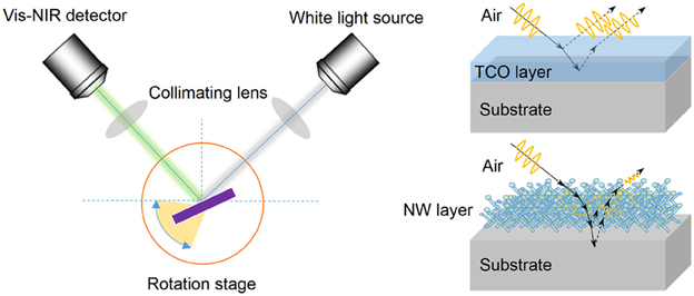
Figure 1. Left: schematic of the angle-resolved reflectance setup. Right: schematic representation of thin film interference that cause reflections between two materials of different refractive indices. Here, the reflections from both interfaces interfere. For the NW coated surface, the graded refractive index from the air with multiple photon scattering and absorption at certain wavelengths allows a suppression of the reflections from the substrate interface that cannot interfere with the remnant intensity of light that reflects within the output light cone. The rough, graded index top surface enhances absorption and aids in broadband antireflection.
Charge transport measurements of the NW layers were conducted using 4-probe measurements using a an Agilent 34401A Digital Multimeter. Measurements were made in 4-probe and van der Pauw geometry. Liquid metal contacts were made using In-Ga eutectic blown into a sphere from a borosilicate capillary glass tube with internal metallization ensuring good wetting (several mm 2) of the NW topology.
3. Results and Discussion
3.1. Growth of Conductive ITO NW Layers
We have developed a simple, reproducible and controllable molecular beam epitaxial growth system for obtaining high quality, uniphasic, branched ITO nanowires on silicon and glass surfaces using In and Sn precursors in an oxygen atmosphere. In addition, the method also allows the growth of polycrystalline porous thin films of ITO. The NWs layer morphology and transparency can be tailored through rational control of the evaporation-condensation parameters, and will be shown to result in bottom-up grown layers of self-catalysed and seeded NWs with excellent electrical, optical and homogeneous structural properties, that can even be grown as large area (several cm2) layers. This is a bottom-up process without requiring oblique angle deposition (OAD) and has a defined grading of the porosity due to the volume fraction linked to defined branching which itself is defined by the crystal growth habit of the material.
Figure 2 shows the range of film morphologies possible by controlling the deposition rate, oxygen partial pressure, the In:Sn ratios and the substrate temperature during molecular beam epitaxial growth on either substrate. In this case, the NWs are examined at the same location, i.e., at the centre of each substrate so that morphology differences are specifically a function of the deposition parameters and not variations in vapor transport and condensation for a given set of parameters. A transition from thin film to porous thick film to high aspect ratio NW layers is characteristically found at higher substrate temperatures and deposition rates for In:Sn ratios nominally of 90:10.
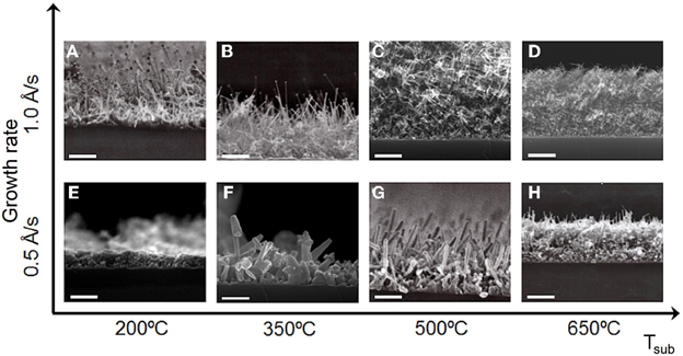
Figure 2. Morphological variation of MBE grown nanostructured ITO layers. Cross-sectional FESEM images of ITO nanowire layers deposited on silicon as a function of deposition rate and temperature of the Sn precursor. A transition from film growth to NWs arrays with decreasing average NW diameter is clearly observed with increasing temperature and deposition rate. For all structures, the In:Sn ratio (90:10) was evaporated at growth rates in the range 0.2–2 Å s−1 at a temperature for In and Sn of TIn = 835°C, TSn = 1000°C, respectively in an oxygen pressure of 2.1 × 10⁻⁴ mbar. Nanowires range between 8 and 50 nm. Substrate temperatures, Tsub, for images (A–D) (grown at a nominal rate of 1.0 Å s−1) and (E–H) (grown at nominal rate of 0.5 Å s−1) are as follows: Tsub = 200, 350, 500, and 650°C, respectively. Scale bars represent 200 nm.
ITO layers were initially grown on oxidized silicon substrates to optimize the experimental growth characteristics and the determine their structure. At low deposition rates and substrate temperatures, the kinetically-driven growth results in the formation of liquid In-Sn alloy nanoparticle droplets that progressively form a continuous layer (29), shown in the cross-sectional TEM and plan-view SEM images in Figure 3A. Oxidative crystallization of this initial deposit provides a near compact conducting wetting layer of ITO of uniform thickness of ~25 nm. Figure 3B shows a cross-sectional TEM image of the ITO thin film deposited at a rate of 0.2 Å s−1 at a substrate temperature of 350°C on Si. The corresponding dark field TEM image of the same region of examination confirms the monocrystalline nature of the layer, where individual grain sizes range from 5–15 nm. Continued deposition results in a thickening of the layer and subsequent formation of voids and continued preferential growth over a surface with a dynamic increase in roughness, as seen in the FESEM image in Figure 3B. The onset of this non-planar morphology occurs at thicknesses >75 nm. Similar morphologies were observed for a range of growth temperatures between 200 and 350°C; the degree of crystallinity increased with temperature. The associated XRD pattern of a series of ITO layers grown at 350°C to different thicknesses in the range 20–400 nm is shown in Figure 3C. The phase can be indexed to the In2O3 structure (JCPDS card 4-0416). These thick porous films have a characteristic (400) texture, typical of the cubic structure. Spectroscopic ellipsometry evidence a refractive index for such layers to be in the range 2.01–2.15. The X-ray diffraction data demonstrate the increase in crystallinity with a corresponding increase in ITO layer thickness. Nucleation and growth is such that a thin ITO layer with a preferred orientation of (222) is initially formed. Subsequent thickening (>150 nm) results in a dominant (400) preferred orientation for layer; the relatively high degree is crystallinity is evidenced by the multiple Bragg reflections from the bulk of the 300 nm-thick ITO layer.
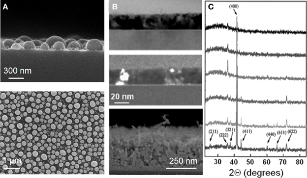
Figure 3. SEM, TEM and XRD measurements of thin, porous ITO layers. (A) Cross-sectional and plan-view SEM images of ITO nanoparticles on silicon during initial MBE growth. (B) Bright field TEM image of a 25 nm thick ITO layer formed after continued deposition beyond the stage shown in (A). The corresponding dark field image underneath acquired along the [100] zone axis shows crystallites within the film. The SEM image underneath shows a 300 nm thick ITO layer with increased surface roughness and internal porosity similar to OAD. (C) X-ray diffraction patterns of a series of ITO layers varying in thickness from 25 nm (top) to 300 nm (bottom).
An increase in the growth rate from 0.23 to 1.33 Å s−1 leads to a transition from thin, relatively compact layers with increasing surface roughness as a function of thickening, to the formation of NWs, which nucleate and grow over the initial compact layer. A nanostructured ITO layer grown at a rate of 1.29 Å s−1 can be seen in the TEM image in Figure 4A. EDX measurements in Figure 4B confirm the In-Sn-O composition and the XRD data in Figure 4C confirms the phase as ITO, with peak broadening characteristic of the reduced crystallite size compared to the bulk thin film material. As with the thick porous films, the ITO layer contains a (222) texture, but this remains dominant since the NWs grow from nanoparticles with a (111) surface termination. We previously confirmed through electron back scattered diffraction that these nanoparticles grow with their (111) planes parallel to the substrate (10). Electron diffraction measurements shown in Figure 4D show that the NWs are composed of monocrystalline (In1.875Sn0.125)O3, in good agreement with the TEM measurements of the thinner layers. These NWs typically have diameters of 8–20 nm and lengths of 40–50 nm for a corresponding nominal film thickness of 60 nm, evidenced in the TEM image in Figure 4D. The associated dark field TEM image in Figure 4D highlights the monocrystalline nature of the NWs throughout their length. The NW layer is branched throughout, with each wire terminated with a phase-similar nucleation seed. The initial grainy layer is a common feature of all deposited oxides, irrespective of the growth rate used. At low deposition rates, the growth is dominated by a layer-by-layer thickening, while at higher deposition rates, NWs form (Figures 4E,F) as a layer. At growth rates between 0.2 and 1.3 Å s−1 it is possible to obtain reasonably consistent thickness layers comprising a majority (>95%) of NWs due to branching events from primary NWs.
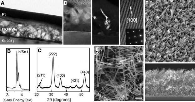
Figure 4. (A) TEM image of a region of the ITO NW layer at early stages of NW growth showing the porous nature of the deposit stemming from the seed layer on the Si surface. (B) Large area EDX spectrum acquired after early stages of NW growth showing the In and Sn L-edge lines, O and Si substrate lines of (In1.875Sn0.125)O3. (C) XRD pattern for early stages of NW growth indexed to the (In1.875Sn0.125)O3 crystalline structure. (D) Bright and dark field TEM images of the early stage of NW growth from the homogeneous In-Sn-O nucleation seeds on the Si surface. (E,F) High magnification FESEM images of the branched ITO NWs structure inside the layer. the plan view and cross-sectional image to the right show the overall morphology of the ITO NW layer as-deposited.
The growth rate and temperature are key parameters in the eventual morphology of the ITO NW layers, and these effects on morphology for a defined composition are summarised in Figure 4, where consistently finer NWs are found at the higher growth rates and temperatures for a given composition, giving a gamut of similar structures with various porosities that allow tunable absorption or reflection across the visible range. This distinct growth mode modification from grains to dendritic growth during deposition while the growth parameters remain unchanged, is due to the difference between the growth and vapor deposition rates. Using effusion cells for the atomic sources in the growth chamber, the shutters are regularly kept closed until the temperature in the cells is reached and the pressure in the chamber reverts to a predetermined lower pressure after its initial increase due to heating of the cells (~10−6 mbar). Thus, there is a localized increase in pressure inside the cells. Therefore, the growth rate is noted to be a factor of two higher than the nominal evaporation rate once the shutters are opened. A high evaporation rate reduces the surface diffusion of the impinging atoms and molecules on the substrate surface enabling the growth of a closed layer. After the growth rate reverts to its normal value, diffusion phenomena dominate resulting in the dendritic growth. Radiative heating of the substrate also contributes to the existence of the growth mode of the grainy interface. A detailed report on this and the unique NW formation mechanism will be presented elsewhere.
For NWs, a distinct growth mode modification from compact (but rough and partially porous) layers to dendritic NW growth during deposition is achievable at specific growth rates and substrate temperatures. No heterogeneous catalysts are required and we still observe extremely high quality, defect-free NWs comprising the layers.
3.2. NIR Trasmission and Antireflection Characteristics of a Graded Index NW Layer
In terms of evaluating the improvement afforded by such NW layers as electro-optical materials, the calculated reflectivity at near-normal incidence (10°) as a function of wavelength was determined and is shown in Figure 5A for the ITO NW layer, and an ITO layer also grown by MBE similar to that shown in Figure 3. ITO NW layers on silicon exhibited much lower reflectivity than either dense ITO on silicon or porous ITO layers in the wavelength region of interest, as was previously observed. These ITO NWs can also be grown on glass in the same growth chamber. Antireflection ITO coatings on glass showed similar transmission (5), and a very low sheet resistivity of 15–63Ω/□ over a range of growths. Such high DC conductivities with good transparency have also been found in silver NW networks and a range of carbon based nanostructured deposits in a variety of transparent-electrode applications (6, 30–37). Fresnel reflection typically found in coherent ITO thin films is eliminated due to graded refractive index depicted in Figure 5B from the substrate to the NW layer/ambient interface, where the effective refractive index was measured to vary from 2.19 (close to bulk value for low porosity thin films shown in Figure 5), to 1.04–1.12 at the air interface of the ITO NW layer. The same NW layers analyzed here show that some variation of the effective index at the air interface is found, depending on whether more clumped or less clumped region (c.f. Figure 4) are probed with a collimated beam.
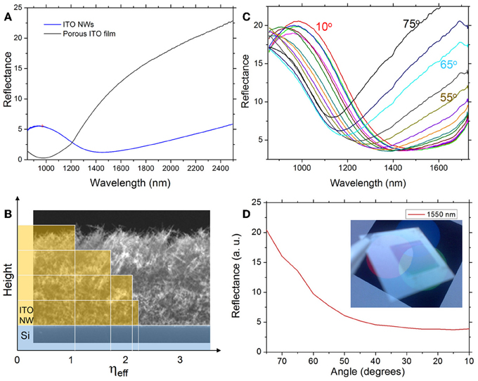
Figure 5. (A) Normal transmission of an ITO NW layer and an MBE grown ITO thin film on glass. (B) Variation of effective refractive index determined from spectroscopic ellipsometry and the Bruggeman effective medium approximation at several stages of NW growth, overlaid on the final structure of a fully grown ITO NW layer. The effective indices shown are calculated at a λ = 1.55 μ m. (C) Angle resolved reflectance measurements of the ITO NW layer shown in (B). (D) The measured reflectance at 1.55 μm as a function of reflectance angle.
For a given angle, the internal optical scattering (a balance of Rayleigh scattering, material absorption and effective medium graded index effects) allows a tunable absorption depending on the NW size, distribution, branching and overall optical morphology. The low refractive index NW layer is optically specular and exhibits a darker surface, confirming the absence of Fresnel reflection over a broad spectral width. This is particularly important for LED applications because of the isotropic emission from the active region and the fact that reflection phenomena can limit the light-extraction efficiency (27, 38, 39).
Typically, ITO and other transparent conducting oxides are much less transparent in the NIR region, thus limiting their employment in the second (1.3 μm) and third (1.55 μm) optical communications energy windows. This is due to the onset of a metal-like behaviour at low photon energies due to the Burstein-Moss shift, but also has contributions where quanta of incident electromagnetic radiation can couple to plasma oscillations. The total transparency that is fundamentally interlinked with it conductivity; the transition occurs on or around its plasma frequency ωp related to the electron density according to the Drude-Sommerfeld model by ω2p = (ne2μ0μr)/m*η2eff, where m* and q are the effective mass and charge of an electron, μr is the relative magnetic permeability the free-space, and ηeff is the effective refractive index determined at the NW-air interface. The surface plasmon resonance of ITO is observed at a much lower energy than for metals (where it generally falls into the visible range). In Figure 5C, the surface plasmon resonance of the ITO NW layer compared to a thin ITO film is red-shifted by ≈500 nm. An example of the antireflective ITO NW on glass is seen in Figure 5D. Reflectance is thus red-shifted into the near-to-mid IR, origin transparency where thin film ITO typically becomes much less transparent, without a sacrifice in electrical conductivity.
The oscillation is characteristic of a well ordered deposit and typically found for thin film interference effects. In the case of reflections at two interfaces, the electric fields from wave optics for light reflection the NW layer-silicon interface and that at the NW layer-air interface can be expressed as:
where k is the wavevector and Cair and CSub are the amplitudes of the waves and their modulus represents the corresponding reflectivity at the NW-air interface, and the NW-substrate interface respectively, according to the three-phase Fresnel equations. ϕ represents the optical path length variation and is proportional to the film thickness. The total intensity is the modulus of both waves
where ϕ = 2ηkdcosαr with η being the refractive index and αr the angle of refraction within the NW layer. These equations predict a suppression of interference effects due to refractive index contrast as the reflectivity (C2air), which is not based on thickness, is minimized. Essentially, the prefactor I0 is the sum of the two reflectivity values and a is given by 2(Cair · CSub)2/(Cair + CSub). The minimum in reflectivity (<5%) is found in between 1.2 and 1.6 μm at near-normal incidence (0–10°), which is shown in the angle-resolved reflectance data in Figures 5C,D. Angle-resolved reflectance measurements show that the position of the surface plasmon resonance blue-shifts with increasing angle; the window for maximum transmission over the widest wavelength range is observed near-normal to the surface and the wavelength range between the effective band-gap as described considering the Burstein-Moss shifts and the expected Drude absorption at longer wavelengths, is increased.
Finally, the roughness and impedance matching at the air interface is demonstrated to enhance antireflection effects, as shown in the inset to Figure 5D, where an ITO NW layer on glass improves transparency through Fresnel reflection minimization. Thus, the optical benefits of porosity afforded by the NW growth offsets the standard trade-off between high transparency and low conductivity (and vice versa) by extending conductive transparency into the infra-red, while allowing tunability in the absorption and angle dependent antireflection through porosity engineering by MBE.
The degree of porosity control by MBE, or any bottom up growth method, largely depends on the growth mechanism of the material on particular substrates, the method of growth etc. Top down methods rely on an understanding of controllably removing the material in 1, 2 or 3 dimensions. In general, the choice of bottom-up or top-down porosity engineering depends on all parameters - bottom up growth typically involves adding the chosen material which infers additional complexity in the control of fill factors and overall porous geometry (random or ordered). In MBE and other physical vapor methods, porosity control largely depends on the nucleation of structures that do not conformally cover a surface and a deposition rate that is fast enough to continue growth in one direction over another. This can be accomplished by oblique angle deposition, or by controlling the kinetics of nucleation, crystallization, growth and continued deposition of a material system. These parameters are also highly dependent on the surface on which the material is grown. Overall, bottom up methods to reproducibly form controlled porous structures are now becoming possible, but predicting which system can achieve a defined porous geometry however, is is rather difficult. Molecular beam and vapor phase epitaxial growth at least maintains a high crystalline and compositional uniformity, with the benefit of a large body of knowledge on how the growth can influence the density (number of individual features) of a material on a surface.
Nanoporous materials, assemblies and films do provide low dielectric constant materials that are required in many areas of microelectronics and photonics. Enabling porosity is the primary route to materials with refractive indices less than 1.2, a necessary objective for a wide variety of optical devices involving photonic crystals, broadband absorbers, omnidirectional reflectors, and better antireflection coatings with tunable transparency windows. Their benefits, however, could extend into biomedical investigations, thermoelectrics, water purification, gas sensing and a variety of other uses.
4. Conclusions
Molecular beam epitaxy was used to grow defect-free self-catalysed ITO NWs as as graded refractive index layers on silicon and on glass. The geometry of the graded porosity ITO NW layers minimizes reflection by randomizing scattering photons and gradually reducing the effective refractive index towards the lower index interface, that of air (or a liquid or polymer encapsulant if that is the impedance matching required). This has allowed a nominally visibly transparent material to maintain excellent transparency (<5% reflectivity) up to 1.6 μm by a shift in the plasma frequency, while retaining good conduction properties. The transmission is both maximized and limited to near-normal output. The optical and electrical properties widen the transparency window for conductive, transparent oxides without the need for complex deposition of several defect-free layers of reducing refractive index or oblique angle deposition. These high crystal quality and self-seeded NW layers also exhibit antireflection properties by eliminating Fresnel reflections at one of the high index contrast interfaces. The method could be extended to any material to reduced interfacial reflection, but to a a range of other transparent oxides to widen the frequency range for transparency, and possibly too for enhancing light extraction efficiencies in light emitting devices.
Conflict of Interest Statement
The authors declare that the research was conducted in the absence of any commercial or financial relationships that could be construed as a potential conflict of interest.
Acknowledgments
Funding: The authors acknowledge support from Science Foundation Ireland under award no. 07/SK/B1232a, the UCC Strategic Research Fund, and from the Irish Research Council New Foundations Award 2012. C. M. Sotomayor Torres thanks the Spanish MINECO project TAPHOR. Part of this work was carried out while she was at the University of Wuppertal and at University College Cork (NMRC-Tyndall).
References
2. Wan Q, Dattoli EN, Fung WY, Guo W, Chen Y, Pan, X., et al. High-performance transparent conducting oxide nanowires. Nano Lett. (2006) 6:2909–15. doi: 10.1021/nl062213d
3. Sawada M, Higuchi M, Kondo S, Saka H. Characteristics of indium-tin-oxide/silver/indium-tin-oxide sandwich films and their application to simple-matrix liquid-crystal displays. Jpn J Appl Phys. (2001) 40:3332–36. doi: 10.1143/JJAP.40.3332
4. Kim H, Horwitz JS, Kim WH, Kafafi ZH, Chrisey DB. Highly oriented indium tin oxide films for high efficiency organic light-emitting diodes. J Appl Phys. (2002) 91:5371–6. doi: 10.1063/1.1461068
5. O'Dwyer C, Szachowicz M, Visimberga G, Lavayen V, Newcomb, SB, Torres CMS. Bottom-up growth of fully transparent contact layers of indium tin oxide nanowires for light emitting devices. Nat Nanotechnol. (2009) 4:239–44. doi: 10.1038/nnano.2008.418
6. Armstrong NR, Veneman PA, Ratcliff E, Placencia D and Brumbach M. Oxide contacts in organic photovoltaics: characterization and control of near-surface composition in indium-tin oxide (ITO) electrodes Acc Chem Res. (2009) 42:1748–57. doi: 10.1021/ar900096f
8. Granqvist CG, Hultker A. Transparent and conducting ITO films: new developments and applications. Thin Solid Films (2002) 411:1–5. doi: 10.1016/S0040-6090(02)00163-3
9. Kim DW, Hwang IS, Kwon SJ, Kang HY, Park KS, Choi YJ. et al. Highly conductive coaxial SnO2-In2O3 heterostructured nanowires for Li ion battery electrodes. Nano Lett. (2007) 7:3041–45. doi: 10.1021/nl0715037
10. Osiak M, Khunsin W, Armstrong E, Kennedy T, Torres CMS, Ryan KM. et al. Epitaxial growth of visible to infra-red transparent conducting In2O3 nanodot dispersions and reversible charge storage as a Li-ion battery anode. Nanotechnology (2013) 24:065401-1–065401-10. doi: 10.1088/0957-4484/24/6/065401
11. Cui Y, Lieber CM. Functional nanoscale electronic devices assembled using silicon nanowire building blocks. Science (2006) 291:851–53. doi: 10.1126/science.291.5505.851
12. Hsu YJ, Lu SY. Vapor-solid growth of Sn nanowires: growth mechanism and superconductivity. J Phys Chem B. (2005) 109:4398–403. doi: 10.1021/jp046354k
13. Zhou J, Liu1 J, Wang X, Song J, Tummala R, Xu NS. et al. Vertically aligned Zn2SiO4 nanotube/ZnO nanowire heterojunction arrays. Small (2007) 3:622–26. doi: 10.1002/smll.200600495
14. Lu JG. Chang P. Fan Z. Quasi-one-dimensional metal oxide materials - Synthesis, properties and applications, Mater Sci Eng R. (2006) 52:49–91. doi: 10.1016/j.mser.2006.04.002
15. Roos N, Sidiki TP. Seekamp J., Sotomayor Torres CM. “Self-organised growth of Indium-Tin-oxide Nanowires,” in Proceedings of the 14th International Winter School/Euroconference on Electronic Properties of Novel Materials Molecular Nanostructures, eds H Kuzmany, J Fink, M Mehring, S Roth (Kirchberg, Tirol: American Institute of Physics (CP 544)) (2000), 419–22.
16. Johnson MC, Aloni S, McCready DE, Bourret-Courchesne E. Controlled vapor-liquid-solid growth of indium, gallium, and tin oxide nanowires via chemical vapor transport. Cryst Growth Des. (2006) 6:1936–41. doi: 10.1021/cg050524g
17. Nguyen P, Ng HT, Kong J, Cassell AM, Quinn R, Li J. et al. Epitaxial directional growth of indium-doped tin oxide nanowire arrays. Nano Lett. (2003) 3:925–8. doi: 10.1021/nl0342186
18. Xiang J, Lu W, Hu Y, Wu Y, Yan H, and Lieber CM. Ge/Si nanowire heterostructures as high-performance field-effect transistors. Nature (2006) 441:489–93. doi: 10.1038/nature04796
19. Law M, Greene LE, Johnson JC, Saykally R, Yang PD. Nanowire dye-sensitized solar cells. Nat Mater. (2005) 4:455–9. doi: 10.1038/nmat1387
20. Dattoli EN, Wan Q, Guo W, Chen Y, Pan X, and Lu W. Fully transparent thin-film transistor devices based on SnO2 nanowires. Nano Lett. (2002) 7:2463–9. doi: 10.1021/nl0712217
21. Wang DL, Lieber CM. Inorganic materials: nanocrystals branch out. Nat Mater. (2003) 2:355–6. doi: 10.1038/nmat908
22. van der Pauw LJ. A method of measuring specific resistivity and Hall effect of discs of arbitrary shape. Philips Res Repts. (1958) 13:1–9.
23. Wan Q, Feng P, Wang TH. Vertically aligned tin-doped indium oxide nanowire arrays: epitaxial growth and electron field emission properties. Appl Phys Lett. (2006) 89:123102–4. doi: 10.1063/1.2345278
24. Zhang L, Tu R, Dai HJ. Parallel core-shell metal-dielectric-semiconductor germanium nanowires for high-current surround-gate field-effect transistors. Nano Lett. (2006) 6:2785–9. doi: 10.1021/nl061833b
25. Nguyen P, Ng HT, Yamada T, Smith MK, Li J, Han J. et al. Direct integration of metal oxide nanowire in vertical field-effect transistor. Nano Lett. (2004) 4:651–7. doi: 10.1021/nl0498536
26. Ju S, Facchetti A, Xuan Y, Liu J, Ishikawa F, Ye P. et al. Fabrication of fully transparent nanowire transistors for transparent and flexible electronics. Nat Nanotech. (2007) 2:378–84. doi: 10.1038/nnano.2007.151
27. Kim JK, Chhajed S, Schubert MF, Schubert EF, Fischer AJ, Crawford MH. et al. Light extraction enhancement of GaInN light emitting diodes by graded refractive index indium tin oxide anti-reflection contact. Adv Mater. (2008) 20:801–4. doi: 10.1002/adma.200701015
28. Lee JY, Connor ST, Cui Y, Peumans P. Solution-processed metal nanowire mesh transparent electrodes. Nano Lett. (2008) 8:689–92. doi: 10.1021/nl073296g
29. Osiak MJ, Armstrong E, Kennedy T, Torres CMS, Ryan KM, O'Dwyer, C. Core-shell tin oxide, indium oxide, and indium tin oxide nanoparticles on Si with tunable dispersion: electrochemical and structural characteristics as a hybrid Li-ion battery anode. ACS Appl Mater Interfaces (2013) 5:8195–202.
30. De S, Higgins TM, Lyons PE, Doherty EM, Nirmalraj PN, Blau WJ, et al. Silver nanowire networks as flexible, transparent, conducting films: extremely high DC to optical conductivity ratios. ACS Nano (2009) 3:1767–74. doi: 10.1021/nn900348c
31. Wu Z, Chen Z, Du X, Logan JM, Sippel J, Nikolou M. et al. Transparent, conductive carbon nanotube films. Science (2004) 305:1273–6. doi: 10.1126/science.1101243
32. Zhang M, Fang S, Zakhidov AA, Lee SB, Aliev AE, Williams CD. et al. Strong, transparent, multifunctional, carbon nanotube sheets, Science (2005) 309:1215–9. doi: 10.1126/science.1115311
33. Chen PC, Shen G, Chen H, Ha YG, Wu C, Sukcharoenchoke S. et al. High-performance single-crystalline arsenic-doped indium oxide nanowires for transparent thin-film transistors and active matrix organic light-emitting diode displays. ACS Nano (2009) 3:3383–90. doi: 10.1021/nn900704c
34. Wu H, Hu L, Carney T, Ruan Z, Kong D, Yu Z. et al. Low reflectivity and high flexibility of tin-doped indium oxide nanofiber transparent electrodes. J Am Chem Soc. (2011) 133:27–9. doi: 10.1021/ja109228e
35. Wu J, Agrawal M, Becerril HA, Bao Z, Liu Z, Chen Y. et al. Organic light-emitting diodes on solution-processed graphene transparent electrodes. ACS Nano (2010) 4:43–8. doi: 10.1021/nn900728d
36. Chiu CH, Yu P, Chang CH, Yang CS, Hsu MH, Kuo HC. et al. Oblique electron-beam evaporation of distinctive indium-tin-oxide nanorods for enhanced light extraction from InGaN/GaN light emitting diodes. Opt Exp. (2009) 17:21250–6. doi: 10.1364/OE.17.021250
37. Guo EJ, Lu HB, He M, Jin KJ, and Yang, GZ. Low-noise solar-blind photodetectors based on LaAlO3 single crystal with transparent indium-tin-oxide electrode as detection window. Appl Opt. (2010) 49:5678–81. doi: 10.1364/AO.49.005678
38. Riedel B, Kaiser I, Hauss J, Lemmer U, and Gerken M. Improving the outcoupling efficiency of indium-tin-oxide-free organic light-emitting diodes via rough internal interfaces. Opt Exp. (2010) 18:A631–9. doi: 10.1364/OE.18.00A631
Keywords: nanowires, transparency, conductivity, indium tin oxide, MBE, antireflection, refractive index
Citation: O'Dwyer C and Sotomayor Torres CM (2013) Epitaxial growth of an antireflective, conductive, graded index ITO nanowire layer. Front. Physics 1:18. doi: 10.3389/fphy.2013.00018
Received: 16 July 2013; Paper pending published: 30 August 2013;
Accepted: 17 September 2013; Published online: 08 October 2013.
Edited by:
Lev Shchur, Landau Institute for Theoretical Physics, RussiaReviewed by:
Joan J. Carvajal Marti, Universitat Rovira i Virgili, SpainRiccardo Sapienza, King's College London, UK
Copyright © 2013 O'Dwyer and Sotomayor Torres. This is an open-access article distributed under the terms of the Creative Commons Attribution License (CC BY). The use, distribution or reproduction in other forums is permitted, provided the original author(s) or licensor are credited and that the original publication in this journal is cited, in accordance with accepted academic practice. No use, distribution or reproduction is permitted which does not comply with these terms.
*Correspondence: Colm O'Dwyer, Department of Chemistry, University College Cork, Cork, Ireland e-mail: c.odwyer@ucc.ie