Role of activation energy in resistance drift of amorphous phase change materials
 Martin Wimmer
 Matthias Kaes
 Christian Dellen
 Martin Salinga
- Institute of Physics (1A): Physics of New Materials, RWTH Aachen University, Aachen, Germany
The time evolution of the resistance of amorphous thin films of the phase change materials Ge2Sb2Te5, GeTe and AgIn-Sb2Te is measured during annealing at T = 80°C. The annealing process is interrupted by several fast temperature dips to determine the changing temperature dependence of the resistance. This procedure enables us to identify to what extent the resistance increase over time can be traced back to an increase in activation energy EA or to a rise of the prefactor R*. We observe that, depending on the material, the dominating contribution to the increase in resistance during annealing can be either a change in activation energy (Ge2Sb2Te5) or a change in prefactor (AgIn-Sb2Te). In the case of GeTe, both contribute about equally. We conclude that any phenomenological model for the resistance drift in amorphous phase change materials that is based on the increase of one parameter alone (e.g., the activation energy) cannot claim general validity.
Introduction
Memory technologies based on phase change materials have been anticipated to fill a technological gap between DRAM and Flash as a fast, non-volatile memory technology [1, 2]. These memory technologies are based on the large resistivity contrast between the two phases of the active material—mostly chalcogenide alloys such as Ge2Sb2Te5. In addition, the ability to switch reversibly [3, 4] and quickly [5] between the two phases by the application of electrical stimuli renders these materials good candidates for electrical data storage. Herein, the crystalline, low resistance (SET) state is reached from the amorphous, high resistance (RESET) phase via an electrical breakdown effect (“threshold switching”) followed by Joule-heating and subsequent fast crystallization, whereas the RESET state is reached by melting the material with a large current followed by rapid cooling (“melt-quenching”).
In a phase change memory cell, the resistance of the cell depends on how much material is amorphous and how much is crystalline. In principle, a variation of the amorphous volume enables the storage of multiple resistance states in a single cell. This way the storage density of the memory could be greatly increased [6–11]. In practice, the phenomenon of resistance drift, i.e., the change of resistivity of amorphous phase change materials over time, precludes a simple implementation of the multibit storage on a chip level.
The increase of resistance of phase change memory devices over time has been found to follow the form of a power-law [12]. Furthermore, it is known that the optical bandgap of thin films of amorphous phase change material opens while the resistance drifts [13, 14]. Also, a change of thermopower with time has been measured on thin films of amorphous phase change materials [15]. And finally, the temperature dependence of the resistance in both thin films and phase change memory cells has been observed to change during drift [16, 17].
Despite all of this experimental evidence, the origin of resistance drift in amorphous phase change materials has so far remained elusive. Irrespective of how an amorphous state was formed, either by melt-quenching (as in devices) or by condensation (in various deposition methods), it is not an equilibrium phase. Thus, it is prone to structural relaxation as is the case for all amorphous materials. In amorphous silicon, amorphous carbon and metallic glasses structural relaxation has been characterized by numerous techniques [18–23]. It is therefore not clear a priori whether the resistance drift observed in phase change materials is a material specific phenomenon or rather a general consequence of the materials being glasses.
Several attempts have been made at providing phenomenological models for structural relaxation leading to resistance drift in phase change materials. In order to connect the resistance increase to changes in the electronic density of states, the valence alternation pair defect model—formerly developed for materials containing chains of chalcogen atoms [24]—has been applied to phase change materials [12]. In their model the authors proposed that upon relaxation neutral defects decay into positively and negatively charged defects resulting in a shift of the Fermi level to midgap and thus an increase in the activation energy of conduction.
Ielmini et al. [25–27], Lavizzari et al. [28] developed a model in which the transport mechanism is assumed to be thermally assisted hopping between electronic defects. In order to describe the change in the low-field resistance over time, the authors postulated an increase in the hopping distance resulting from an annihilation of electronic defects upon structural relaxation. In this model, the postulated decrease in defect density also leads to an increase in activation energy.
A divergent explanation was proposed by Karpov et al. [29], suggesting a volume change of the amorphous phase change material due to differences in the volumetric mass densities of the amorphous and the crystalline phase (~6%) to be responsible for drift. By employing the general concept of the double-well potential for the atomic potential of metastable glasses to chalcogenide alloys [30] and the resulting relaxation characteristics the authors proposed a correlation between volume change of the amorphous phase and the time evolution of the resistance [29].
On a phenomenological level, attempts have previously been made [31] to connect the increase in resistance over time R(t) to an increase in the activation energy of conduction EA(t).
R* is the pre-exponential factor in the Arrhenius law, kB the Boltzmann constant and T the annealing temperature.
This link was supported by experiments in which the RESET state of mushroom-type cells of Ge2Sb2Te5 was annealed to different temperatures and the resistance was determined at three different points in time after RESET. The authors were able to describe their data by a change in the activation energy alone and thus, it seemed that a change of the prefactor R* could be completely neglected.
In contrast to that, temperature dependent resistance measurements performed on cells of the line-cell type based on doped Sb2Te [32] yielded the result that the increase of resistance observed on the corresponding RESET state could only be explained by an increase of both the prefactor and the activation energy. Unfortunately, the composition of the material in these phase change memory cells investigated was not made public.
In this work we repeatedly measure the temperature dependence of resistance to characterize the temporal evolution of EA and R* upon drift at a constant annealing temperature for several phase change materials. By choosing the materials Ge2Sb2Te5, and AgIn-doped Sb2Te (more precisely Ag4In3Sb67Te26) we furthermore aim at studying the apparent contradiction between the two aforementioned experiments [31, 32]. The third material, GeTe, is studied due to its promising switching characteristics [5]. In the literature the majority of experiments are done in melt-quenched amorphous phase change memory cells. These previous studies showed that different read out voltages and currents as well as varying RESET states can all influence the resistance drift behavior [10, 25, 27, 29, 33, 34]. Former works also indicated a potential influence of the surrounding dielectric material encapsulating the phase change material in a cell on the drift behavior [35]. Furthermore, the shape of the melt-quenched amorphous plug inside a memory cell can be non-trivial, which affects the electrical field distribution and the total cell resistance. Finally, the polycrystalline phase change material surrounding the amorphous volume is also known to change its structure and electronic properties upon annealing [36, 37]. All these artifacts can change from one device architecture to another. The different observations of the temporal evolution of EA and R* reported in Boniardi et al. [31] and Oosthoek et al. [32] can either be related to the above mentioned artifacts in nano-scaled devices or to intrinsic material properties. It is therefore desirable to exclusively measure the pure material properties of the amorphous phase change material of interest. Hence, in the present work we investigate fully amorphous phase change thin films. Measurements on such samples are performed at very low electrical fields and current densities. The use of as-deposited amorphous material guarantees a reproducible initial state of the sample before starting the measurement. As a consequence, our measurements on sputtered thin film samples and the conclusions to be drawn from them are not affected by variations of the initial state, which are common for studies on memory cells.
Methodology
Heated Van-Der-Pauw Setup
The electrical characterization was performed at a custom-made tester (illustrated in Figure 1), which is capable of measuring resistances up to approximately 1 GΩ. Besides the typical two-point measurements, the setup is able to perform four-point Van-der-Pauw measurements [38] of the sheet resistance. Therefore, a Keithley SMU 236 source measuring unit forces an adjustable current through two contacts on one side of the sample, whereas an Agilent multimeter (type 34401A) measures the voltage drop at the opposite side of the sample. To switch these two instruments between the different contacting needles (necessary for the Van-der-Pauw method) a custom-made electrical switching board was designed to guarantee the lowest possible leakage current in the circuit and thereby enhancing the measurement range and precision.
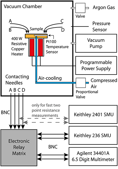
Figure 1. Schematic illustration of the Van-der-Pauw setup. The samples are positioned on top of a temperature controlled copper block inside a vacuum chamber. Before starting the measurement the vacuum chamber is first evacuated and afterwards flushed with pure argon gas. Four 100 W resistive heater cartridges enable us to heat up the sample (e.g., with a rate of 1 K/s) to about 650 K. Whereas, cooling is done by passing compressed air through a small pipe in the copper block. Both the electrical power supply for the heating cartridges and the proportional valve for the compressed air inlet are PID controlled. The electrical contact is realized by four gold-plated and spring-supported needles, which can be moved to different contact pads on the sample. A custom-made electronic relay matrix connects a source-measuring-unit (SMU) and a multimeter to any of the contact needles. For fast two-point resistance measurements a second SMU is directly connected to two of the needles.
The sample is installed in a vacuum chamber on top of a gold-plated copper block (sample holder), which encases four symmetrically arranged 100 W resistive heater elements. All measurements are performed in a clean argon atmosphere at a pressure of 950 mbar within the vacuum chamber. The copper block can additionally be cooled by forcing a cooling agent (compressed air) through an integrated tubing system. The PID controlled system is therefore able to vary the temperature between room temperature and 350°C at a ramp of 1 K/s. The temperature is measured by a Pt-100 sensor, which is positioned directly underneath the copper block surface next to the sample. A good knowledge of the temperature is of great importance for an investigation of the temperature-activated conductivity of phase change materials. Therefore, special care was taken to guarantee an accurate determination of the temperature of the phase change layer (see Section Temperature calibration).
A Labview software controls all instruments of the setup and enables us to perform automated electrical measurements with pre-programmed temperature profiles. Due to the high resistances and the large capacitances (in the range of 100 nF) of the amorphous as-deposited phase change thin films the RC time constant of the electrical setup is in the range of several seconds. Therefore, each time before the Agilent multimeter determines the voltage drop at one side of the sample during a Van-der-Pauw measurement, the setup waits until the parasitic capacitance of the sample is charged and the voltage level saturates. This cancels all parasitic effects in the electrical circuit and makes a correct measurement of the sample resistance possible. However, a drawback of this method is the limited time-resolution, which is about 20–30 s between two measurements of the sheet resistance.
In order to investigate the temporal evolution of the activation energy for conduction and the prefactor in the Arrhenius law, time-resolved drift characterizations were performed as two-point resistance measurements at a constant voltage applied on two of the four contacts. This method strongly improved the time-resolution of the measurement into the range of several 10 ms, since all parasitic capacitances are kept fully charged throughout the whole measurement, so no slow charging-discharging cycles are apparent in the recorded data. Sheet resistance data were only taken once after each series of time-resolved measurements in order to translate the resistance drift data into drift of the specific resistance of the phase change material.
Sample Fabrication
Thin film samples for two-point- and four-point-probe Van-der-Pauw measurements were fabricated on SiO2 glass substrates. Photolithography was used for patterning of the tungsten electrodes and contact pads as well as four metal wire structures (temperature sensors) for measuring the temperature dependent resistance of a tungsten line (see Figure 2). The tungsten electrodes as well as the different phase change materials were deposited by DC magnetron sputtering.
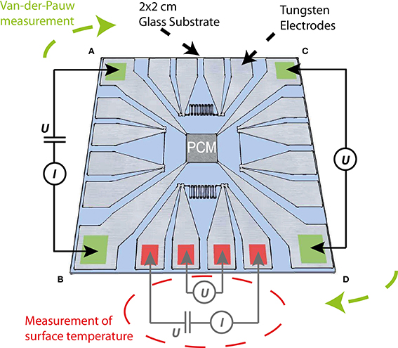
Figure 2. Structure of the phase change thin film samples. The 3.5 × 3.5 mm2 phase change area in the middle of the substrate is contacted by four tungsten electrodes (marked in green), which were patterned at the edges of the 2 × 2 cm2 glass substrate. Besides the Van-der-Pauw structure 10 μm wide tungsten lines are integrated at each side of the substrate (two line and two zig-zag structures). The different tungsten line structures (each electrically contactable via four contact pads) serve as temperature sensors of the surface temperature of the substrate in close proximity to the phase change material.
The SiO2 glass substrates were cleaned at room temperature in a first step within an ultrasonic bath with acetone and subsequently with isopropanol for 15 and 5 min respectively. After dry cleaning of the substrates with nitrogen gas, a layer of 1.3 μm thick AR-U 4040 resist was spin-coated on the substrate and baked at 95°C for 2 min. The electrode design features four contact pads at the edges of the 2 × 2 cm2 SiO2 glass substrates and electrode lines, which connect the contact pads with the 3.5 × 3.5 mm2 area for the film of phase change material in the middle of the substrate. Four metallic, 10 μm wide lines (two straight lines and two zig-zag structures) serving as resistive temperature sensors are each connected by 4 probe pads to enable a precise determination of the line's resistance without any influence of the contact or feed line resistance. Especially for comparably fast temperature changes in the order of 1 K/s the thermal capacitance of the 500 μm thick SiO2 glass substrate could create a difference in temperature between the copper block and the phase change layer on top of the substrate. Therefore, a careful calibration of the actual surface temperature (see Section Temperature calibration) is needed to guarantee unaltered measurements of the temperature dependent resistance of the phase change material. After developing the resist with a mixture of 1 part of AR 300-47 and 2 parts of deionized water the electrode structure and temperature sensors were realized on the substrate.
100 nm of tungsten was deposited by DC magnetron sputtering at a power of 60 W within a high purity argon inert gas atmosphere (argon with built-in purifier (BIP ×50); base pressure after evacuation 2.0 × 10⁻⁴ Pa, total pressure during sputtering 0.5 Pa) to realize the electrodes and temperature sensor lines. The lift-off process was performed immediately after deposition by rinsing with acetone and isopropanol employing a syringe.
In a last step, the phase change material and a suitable capping material, (ZnS)80:(SiO2)20, was sputter deposited in-situ within the same sputtering tool. The capping material serves as a barrier for potential oxidation and outgassing of the phase change material during annealing. Shadow masks were used to define the 3.5 × 3.5 mm2 area for the phase change material. In order to investigate the drift behavior of different phase change materials, layers of 200 nm Ge2Sb2Te5(GST), GeTe and Ag4In3Sb67Te26 (AIST) were deposited in separate sputter processes from stoichiometric targets at a DC power of 20 W. Previous to each sputter process the chamber was pumped down to 1.3 × 10⁻⁴ Pa. Without breaking the vacuum a 40 nm (ZnS)80:(SiO2)20 capping layer was sputtered by RF magnetron sputtering at 60 W on top of the phase change material. The pressure during sputtering was approximately 0.5 Pa in each process.
To minimize the drift effect between sample fabrication and the beginning of the electrical measurements, the samples were welded in a PE-foil in nitrogen atmosphere and stored at (6 ± 1)°C in a refrigerator. The temperature was continuously monitored during storage.
Temperature Calibration
To rule out any corruption of the measured data we first checked the influence of a potential temperature mismatch or delay between the heated copper block and the substrate surface. Therefore, the temperature dependent resistance of the small tungsten lines and the temperature determined by the Pt-100 sensor inside the copper block were measured simultaneously. It turned out that during fast heating ramps (e.g., 1 K/s) the difference in temperature was as much as 0.5 K, whereas during cooling no measurable difference was observed due to the limited cooling rate (0.3 K/s at maximum) of our compressed air cooling setup. Hence, the influence of the heat capacity of the device can be neglected in the following characterization (as only data from cooling processes are analyzed) and the following temperature data originate from the temperature sensor in the copper block.
Results and Discussion
Resistance Drift in Amorphous As-Deposited Phase Change Films
For investigations of the irreversible change in resistance caused by the drift effect in amorphous as-deposited thin films, we heat the sample to the chosen annealing temperature (between 50 and 80°C) and keep this temperature fixed for about 6–12 h. During that period of time the resistance is monitored by Van-der-Pauw measurements. In contrast to many other works [16, 25, 28, 39, 40], the resistance is measured directly during annealing in all the experiments performed within this work.
Typically, the resistance drift effect in amorphous phase change materials is described by an empirically found power law
where R0 is the resistance at the time t0, t the annealing time and v the drift exponent.
This description is valid for melt-quenched amorphous phase change cells, in which the time between amorphization and read-out is well known. We, however, investigate thin layers of amorphous as-deposited phase change material. The formation of this amorphous state differs strongly from the melt-quenching process. In memory cells the amorphous phase is created by freezing three-dimensional atomic rearrangements in the supercooled liquid. In contrast, during sputter deposition single atoms or clusters of atoms with high kinetic energy are adsorbed on the sample. Subsequent rearrangements of deposited atoms into energetically more favorable positions on the surface take place in the presence of condensed matter only in half of their surrounding. Atoms reaching the sample afterwards can induce further rearrangement of the underlying atoms. Therefore, the thermal history of an amorphous as-deposited sample is complex and it is difficult to define a precise moment of amorphization as reference point for the time scale of a resistance drift measurement. Nevertheless, for measurements of amorphous as-deposited samples it has been shown, that the power law can be extended by a virtual age ts of the sample [17].
When annealing an amorphous as-deposited sample to a certain temperature, the virtual age ts indicates the time the sample would have to have drifted at this annealing temperature in order to experience the same change in resistance as took place during storage before starting the measurement. Hence, the virtual age is a measure of the thermal history of a sample. The influence of ts is particularly visible at the beginning of the annealing process (see Figure 3), while at longer times the additional drift due to annealing overshadows the effect of the thermal history. Thus, Equation 2 can account for data at long annealing times (dashed blue line), but only the extended Equation 3 describes the whole dataset nicely (dashed red line).
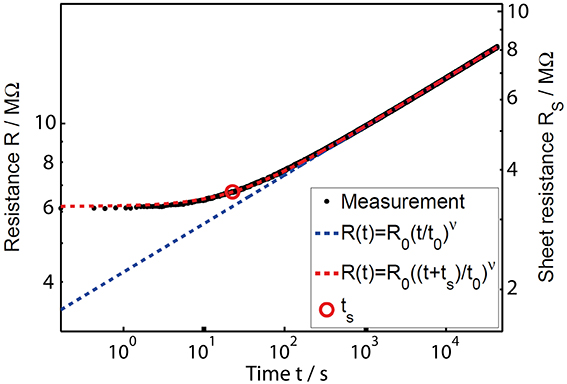
Figure 3. Double logarithmic plot of the resistance drift in amorphous as-deposited GeTe upon annealing at (80.00 ± 0.03)°C. The black raw data points for the resistance were measured via two contacts. A normalization of these data was done with the help of a four-point Van-der-Pauw measurement directly after the drift experiment (leading to the sheet resistance values indicated by the right vertical axis). The common power law (blue dashed line) matches the experimental results well for long annealing times only. An extended power law (red dashed line) taking into account the thermal history of a sample, however, can describe the resistance drift in amorphous as-deposited phase change films over the whole measurement range [17].
In the past the thin-film resistance was plotted vs. the time corrected by the virtual age, t + ts, while ts is handled as a free fit parameter [17]. This modification of raw data results in a straight line in a double logarithmic plot. Here, we propose a different method for analyzing and presenting the time-resolved resistance data, in which the original axes remain intact. We believe that fitting the commonly used power law to data at long annealing times and then calculating the virtual age ts is a more transparent way to treat the data. Thereby, we reduce the amount of fit parameters and do not have to alter the presentation of the raw data. By following this approach, we determine the drift exponent v (together with all other parameters) by fitting Equation 2 to the experimental data at higher annealing times, where the data look sufficiently straight. Now the virtual age ts can be derived from the difference between these fit results, Rpl(t), and the experimental data that actually follow an extended power law, Repl(t), according to the following relationship.
Thus, the time ts (indicated by a red circle in Figure 3) is reached in the moment when the difference between Equations 2 and 3 equals the drift exponent v (derived by fitting at higher annealing times) multiplied by log(2).
Using this procedure, we investigated the resistance drift behavior of three phase change materials (GST, AIST and GeTe) at four annealing temperatures between 50 and 80°C (exemplarily shown in Figure 4 for GeTe). Comparing the absolute values of the sheet resistance data as a function of temperature, a decreasing trend is visible with increasing temperatures, as it is expected for a thermally activated conductivity in a semiconductor. In addition, the pronounced temperature dependence of the virtual age ts can be observed in the temporal evolution of the resistance (Figure 4). For low annealing temperatures (e.g., 50°C) the influence of the sample's thermal history leads to deviations from the pure power law (indicated by the black dashed line) over a longer duration, indicated by a high value in ts. At high temperatures (e.g., 80°C) the resistance drift is strongly accelerated and thus dominates the signal much earlier [16]. Any relaxation prior to annealing is quickly surpassed by the pronounced drift at elevated temperatures. Therefore, for samples with comparable thermal history the virtual age, as it is defined in Equation 3, decreases with increasing annealing temperature.
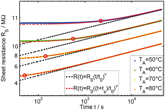
Figure 4. Resistance drift measured in GeTe thin films at annealing temperatures between 50 and 80°C plotted on double logarithmic scale. The dashed lines indicate the fits by the commonly used simple power law (black) and the extended power law (red) to the experimental data (solid lines) at different annealing temperatures. The simple power law was only fitted to data for times much greater than the individual virtual age of the sample (red circles).
Comparing the experimental findings for the three phase change materials (Figure 5), clear differences in the absolute values of v become visible. However, the overall trend in v, R0 and ts as a function of annealing temperature is nearly the same for the three characterized materials. Since the read-out temperature equals the annealing temperature in all our measurements, the drift exponent for resistance shows nearly no temperature dependence for all three materials which is in line with the work of Boniardi et al. [31]. The prefactor R0 of the power law clearly shows a decreasing trend with increasing temperature, which is due to the temperature-activated conductivity of amorphous phase change materials.
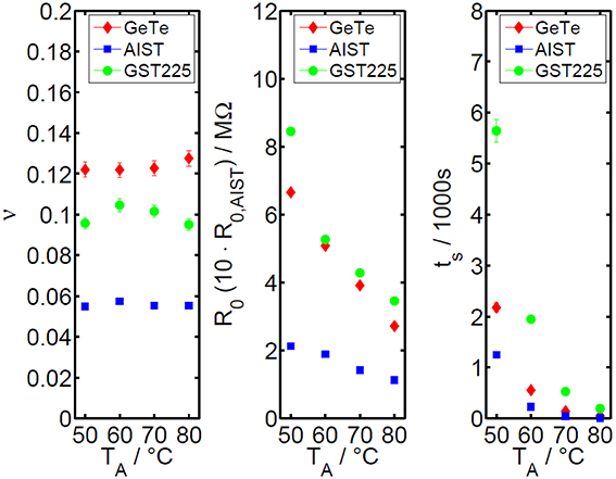
Figure 5. Overview of the extended power law parameters as a function of temperature for GeTe, AIST, and GST. The drift exponent for resistance v (left diagram) is found to be fairly constant for annealing temperatures between 50 and 80°C. The power law prefactor R0 (diagram in the middle) shows a decreasing trend with temperature due to the thermally activated conduction in amorphous phase change materials. (The data for AIST are magnified by a factor of 10 in order to enhance the visibility of the decreasing trend). The diagram on the right depicts the virtual age ts as a function of temperature. The lower the difference between storage and annealing temperature, the higher is the virtual age, since the drift effect during storage has a stronger influence at lower annealing temperatures.
For resistance drift measurements in phase change memory cells it has been reported that electrical bias, read-out current, cell state and geometry chosen in the experiment can change the drift exponent v significantly (Table 1). The absolute values of the drift exponent v determined in this work match quite well to literature data on memory cells in case of GST [16, 17, 31, 34, 41–44] as well as on thin film samples for AIST and GeTe [17, 44] as depicted in Table 1. The difference of the drift behavior between amorphous as-deposited samples compared to the melt-quenched cells seems to be sufficiently treated with the introduction of the virtual age ts. Therefore, the experimental findings within this work can be assumed to be relevant also for the behavior of phase change materials inside of memory cells.
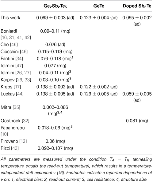
Table 1. Collection of drift parameters for amorphous as-deposited (ad) and melt-quenched (mq) phase change materials.
Drift of Activation Energy for Conduction and Prefactor in Phase Change Thin Films
The main focus of this work is the investigation of the drift in activation energy for conduction for different phase change materials. In a previous work [31] Boniardi et al. showed, that—in case of Ge2Sb2Te5—the drift in resistance can purely be attributed to a change in activation energy. Here, we provide an extended characterization for three phase change materials, namely Ge2Sb2Te5, GeTe and AgIn-doped Sb2Te in order to further illuminate this matter.
According to the work of Oosthoek et al. a physically relevant measure of the activation energy can only be taken during a temperature cooling ramp, when the thermally activated drift effect is strongly hindered [32]. Therefore, the annealing process at a constant temperature of 80°C was repeatedly interrupted after 5 min by a temperature dip (exemplarily shown for GeTe in Figure 6). During each dip the temperature was first decreased as fast as possible to about 40°C and afterwards quickly increased again to reach the initially chosen annealing temperature. The interruption of the annealing process of the sample is therefore kept as short as possible (about 140 s) and the good time-resolution of the two-point resistance measurements enables us to gather a sufficient amount of data during each cooling step. This procedure was repeated over 17 h for each sample to investigate the temporal change in resistance R(t), activation energy EA(t) and prefactor R*(t) (as defined in Equation 1).
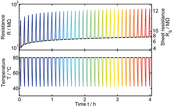
Figure 6. Time-resolved experimental data for the resistance of a GeTe thin film sample (top diagram) as result of the application of a temperature profile (bottom diagram). The drift effect is visible as an increase of the resistance at constant annealing temperature of 80°C (black curve). Due to the semiconducting nature of the amorphous material the resistance strongly increases as the temperature is reduced. The color of the temperature dips reflects the point in time during the drift experiment.
As expected for the drift effect, a continuous increase in resistance is visible over time (black data points in Figure 6). Due to the Arrhenius behavior of the material, a strong change of resistance can be observed whenever the temperature is changed. Due to the modification in the temperature profile the question arises whether the annealing process is still comparable to the usually performed constant annealing temperature experiments. To verify the comparability we only extracted the data measured at a constant temperature of 80°C (Figure 7). The raw data (black) show a significant deviation from the extended power law especially at short annealing times. This issue can be explained by the interruption of the drift process during each temperature dip. Thus, the time axis in Figure 7 does not correspond to the actual annealing any more, leading to a deviation from the power law (where t indicates the annealing time). A valid comparison to the power law behavior can only be done when correcting the time scale so that it reflects solely the duration of the effective annealing at 80°C (green data points). Thus, we neglect any influence to the drift effect coming from temperatures lower than 80°C. While this procedure works well for medium and long annealing times, for very short times (e.g., before the first temperature dip and up to about 30 s in Figure 7) a clearly observable resistance drift is possible even at temperatures lower than 80°C. This can be explained by the first annealing phase (at 80°C) being so short, that some weakly activated structural relaxations remained unexecuted and were realized even with lower thermal energy during the temperature dip. For verification of the comparability at medium and long annealing times, we plotted the extended power law with the same drift exponent as derived earlier for a measurement at constant annealing temperature of 80°C (see Section Resistance Drift in Amorphous as-Deposited Phase Change Films) together with the time-corrected data of the interrupted annealing experiment (red dashed line vs. green data points in Figure 7). Apart from the first 30 s a good agreement between the power law (red dashed line) and the corrected data (green data points) becomes visible, proving unchanged drift behavior. Therefore, the time-resolved measurements of the activation energy presented in the following part can be regarded to be fully comparable with the usually performed constant annealing experiments.
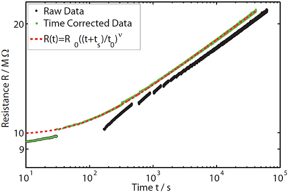
Figure 7. Time-resolved resistance data measured on a GeTe sample at 80°C annealing temperature (black data points). Due to the interruption of the annealing process during the temperature dips, the data do not follow the extended power law (red dashed line). Therefore, the time values of the raw data are corrected to reflect only the duration spent at the constant annealing temperature (green data points). The corrected data fit the previously determined drift exponent of the extended power law (in the constant annealing temperature experiments at 80°C in GeTe) quite well, except for the first 30 s (deviation between green curve and red dashed line). During these first seconds, the resistance drift occurs also at temperatures lower than the annealing temperature (i.e., during the temperature dip) and thus changes the absolute resistance value after the dip. This is why the data taken during the first dip were not taken into account in the data analysis.
For each single temperature dip the logarithm of the resistance is plotted as a function of 1/kBT (Figure 8). In such an Arrhenius plot the slope of the resulting straight line equals the activation energy for conduction EA and its intercept corresponds to the prefactor R* in the Arrhenius law (Equation 1). Values for the temporal evolution of EA(t) and R*(t) are determined by fitting the experimental data for each temperature cooling step within the total time of the experiment of about 17 h. To avoid any influence of the resistance drift effect on the determination of the Arrhenius parameter, the fits are only applied to temperatures starting from 10°C below the maximum annealing temperature down to about 43°C. At these lower temperatures (compared to the annealing temperature) an irreversible increase in resistance is efficiently frozen out for the duration of the temperature dip, because the material already drifted at a higher temperature for some time.
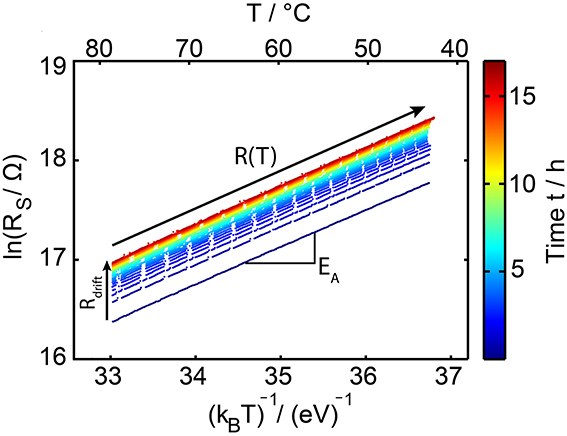
Figure 8. Arrhenius plot of the measured sheet resistance data on GeTe. For each temperature dip a single line is shown. The line color indicates the drift time ranging from several seconds up to about 17 h. Upon drifting (going from dark blue to dark red colors) the straight line continuously shifts to higher values in resistance. The interruptions within each line are due to the limited amount of data which our Keithley SMU can store internally. Time-resolved data for the activation energy of conduction (slope) as well as the prefactor (intercept for T approaching infinity) within the Arrhenius law are determined by fits on the individual curves at the cooling ramp during each temperature dip.
Comparing our findings with the previous work of Boniardi et al. [31], who determined the change in melt-quenched amorphous Ge2Sb2Te5 in memory cells, we are able to reproduce their result of a constant prefactor R* over time (Figure 9, left). According to Boniardi et al. the temporal evolution of the activation energy in case of a constant Arrhenius prefactor can be described in the following way:
Thus, the resistance drift effect in amorphous Ge2Sb2Te5 can be attributed to a change in the activation energy, irrespective of the material being in the form of a thin film or nano-structured devices. This again strengthens the claim of comparability between drift behavior in melt-quenched and as-deposited amorphous phase change material.
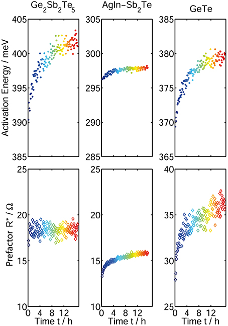
Figure 9. Time-resolved measurement of activation energy (top) and Arrhenius prefactor (bottom) for the phase change materials Ge2Sb2Te5 (left), AgInSb2Te (middle), and GeTe (right). The values are determined by fitting a straight line to the experimental data in the Arrhenius plot. While Ge2Sb2Te5 shows a clear increase only in activation energy but no change in the prefactor, AgInSb2Te and GeTe show an increase in both EA and R*.
In contrast to Ge2Sb2Te5, our measurements on AgInSb2Te and GeTe clearly show a significant change in both the activation energy and the Arrhenius prefactor (Figure 9). The Arrhenius prefactor being constant in the case of Ge2Sb2Te5 seems to be rather an exception than a universal rule for drift behavior in amorphous phase change materials. Thus, the assumptions made by Boniardi et al. leading to Equation 5 [31] are not valid for all amorphous phase change materials. Instead, a general model for drift in phase change materials has to take into account a time dependence of both EA and R*. A possible explanation for these experimental findings could be a change of the temperature dependence of the band gap as proposed in Oosthoek et al. [32]. To validate this hypothesis, however, further experimental evidence is needed, e.g., temperature and time dependent measurements of the optical band gap.
We were able to reproduce all experimental results on the drift in activation energy and prefactor for the three different materials in multiple samples fabricated in different sputter deposition processes. For GeTe we found small changes in the absolute values in EA and R* while the overall trend remains the same. In Wood et al. [48] it was already shown that small variations in stoichiometry in GeTe (~1%) could lead to a large change in activation energy for conduction. These variations could have been created due to slightly different sputter deposition parameters, although all set values (e.g., pressure, power, flux …) are kept constant. Changes in the Argon flux for example (in the range of several sccm) can change the resulting stoichiometry of the sputtered samples. In case of Ge2Sb2Te5 and AgInSb2Te the reproduction of the results presented was possible without any difficulties.
Since the changes in EA and R* are directly linked to the change in resistance (Equation 1), the absolute shift in these parameters must be directly related to the strength of the resistance drift effect (the drift parameter v). For a quantitative evaluation of the strength of the two different contributions it is calculated, how much of the relative change in resistance is due to a change of activation energy and how much due to a change of the prefactor (ΔEA, rel and ΔR*rel in Figure 10). This way an instructive comparison between the three different materials becomes possible. AgInSb2Te only shows a weak increase in EA and R*, which is in line with the low drift exponent for resistance that was derived before in the constant-temperature measurement (Figure 5). In this material the change in R*clearly dominates the drift effect, whereas in GST the opposite is true; the change in EA dominates the overall drift in resistance. The resistance drift can actually be attributed solely to the change in activation energy, while the prefactor remains constant over the whole duration of about 17 h. In the case of GeTe, both components contribute roughly equally to the resistance drift. Also for GeTe the combined relative changes due to temporal increase of activation energy and prefactor is the strongest of all three investigated materials, in accordance with the largest drift exponent v.
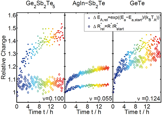
Figure 10. Relative change in resistance due to a change in activation energy and prefactor as a function of drift time for GST, AIST, and GeTe. The relative change due to the change in activation energy is determined by subtracting the initially measured value for EA (determined by the second dip), whereas the relative change due to the prefactor is extracted by a normalization to the value of R* measured in the beginning.
The comparison between GST, AIST, and GeTe shows clearly, that the resistance drift effect cannot simply be explained by a change in one physical parameter, but rather by a material dependent combination of the evolution in activation energy and the prefactor in the Arrhenius law. This way our measurements are able to resolve the disagreement between the works of Boniardi et al. [31] and Oosthoek et al. [32], who - using different types of memory cells—came to differing results about the role of activation energy and prefactor in resistance drift. Our measurements indicate, that the discrepancy between the observations in these studies results from a material dependent difference in the drift behavior rather than from artifacts due to distinct geometries of the memory cells used.
Only a complete description of the changes in the electronic density of states over time together with a coherent transport model will be able to fully clarify the origin of the resistance drift effect. Until then, also the exact mathematical description for the temporal evolution of various parameters must remain open. In view of the results presented it seems promising to aim next at the characterization of the temporal evolution of parameters like band gap, charge carrier mobility, carrier density, trap distributions etc. To serve as a useful reference for future studies we now present several quantitative descriptions of the changes in EA and R* over time that match the experimental data equally well. Future works may show which mathematical description is most appropriate.
The functional dependencies for the temporal evolution of the activation energy and the Arrhenius prefactor in Equations 6 and 7 are motivated from the work of Boniardi et al. [31] and Fugazza et al. [49].
E1, m, R*1 and b are treated as free fit parameters, which could be dependent on the annealing temperature.
While the quantitative descriptions in Equations 6, 7 are able to match the experimental data nicely (Figure 11), the characterized drift process between about 1 s and 17 h still gives leeway for alternative dependencies of the activation energy and the Arrhenius prefactor as a function of time (Equation 8, 9).
In an analog way to Equations 6 and 7 the parameters E2, n, R*2 and b serve as a free fit parameters (fit results can be found in Table 2).
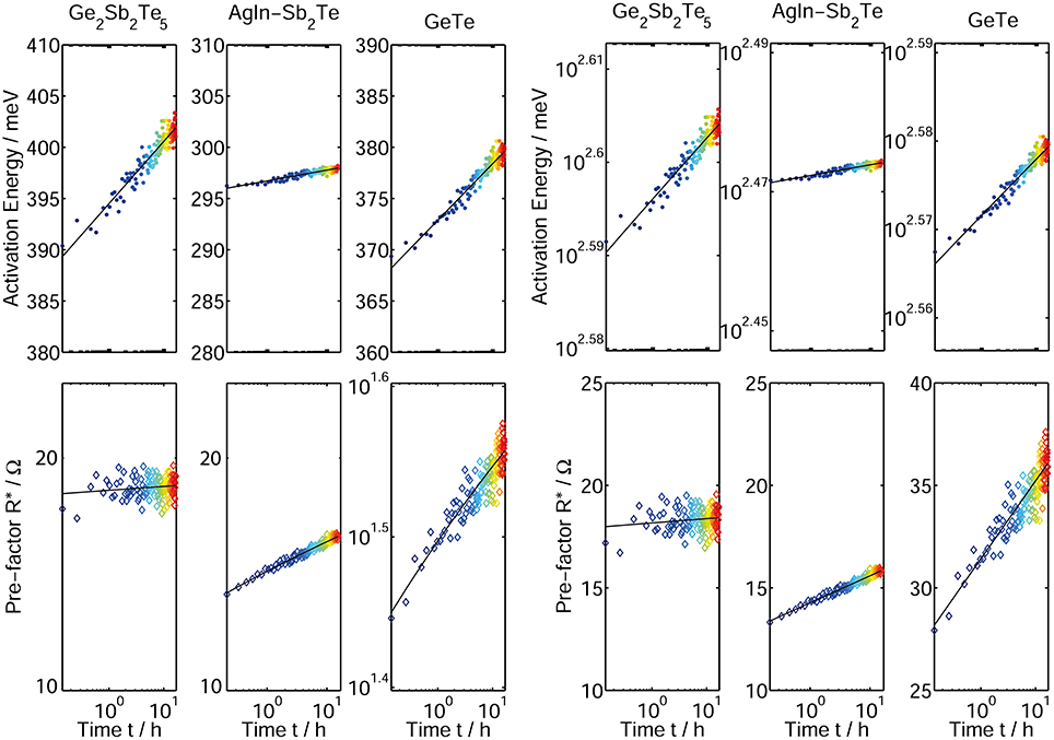
Figure 11. Time-resolved activation energy (top) and Arrhenius prefactor (bottom) plotted on a logarithmic and double logarithmic scale for three phase change materials Ge2Sb2Te5, AgInSb2Te, and GeTe. The fits indicated by the black lines are preformed according to EA(t)~ln(t) and ln(R*(t))~ln(t) (Equations 6, 7) (left) and ln(EA(t))~ln(t) and R*(t)~ln(t) (Equations 8, 9) (right) with t0 set to 1 s. Although the functional dependencies in the Equations 6, 7 and 8, 9 differ, the fit quality in both cases is undistinguishably good. A distinct determination of the algebraic function of EA and R* over time is therefore not feasible with the data presented here.
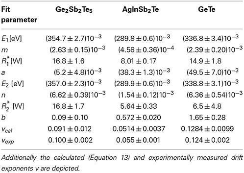
Table 2. Fit parameters for the temporal evolution of the activation energy for conduction and the Arrhenius prefactor according to the Equations 6–9.
It should be noted, that due to the limited measurement time and the small increase in EA and R* the fit quality of Equations 6, 7 (left side of Figure 11) and 8, 9 (right side of Figure 11) shows no significant differences. Therefore, both the activation energy as well as the Arrhenius prefactor could be either parameterized by Equations 6 and 8 or 7 and 9 respectively. From an algebraic point of view the parameterization in Equations 6 and 7 enables the benefit of a calculation of the drift exponent v for resistance, which is presented in the following part.
By comparing the power law to the Arrhenius law (see Equations 10–13), the estimated fit parameters E1, m, R*1 and b (Table 2) and the functional dependencies in Equations 6 and 7 allow for a direct calculation of the drift exponent v.
Comparing values for the resistance drift exponent v (Table 2), the ones that were directly measured match very well to those that were derived from the drift of EA and R* for all materials. This is not a priori clear as the calculated and experimentally measured data for v are not only derived via different experimental procedures with distinct temperature treatments (constant annealing temperature vs. experiments with temperature dips) but also measured on different samples.
From our point of view the equality of v for the experimental and calculated data in all investigated phase change materials serves as an additional indication, that the modified temperature profile does not influence the overall drift effect. Furthermore, it shows that the data obtained in such an experiment are well comparable to those of an annealing experiment performed at a constant temperature. Most importantly, the drift in resistance in different amorphous as-deposited thin film samples can be consistently explained by a temporal change in EA and R*.
Conclusion
In this work we described a method for the investigation of resistance drift in amorphous phase change materials that is capable of measuring the pure material property without the danger of artifacts, which have to be expected when working with memory cells. Despite the use of amorphous as-deposited samples our analysis resulted in insights, which are also technologically relevant for the application of phase change materials in electronic data storage, as proven by the good agreement with literature on drift characteristics of memory devices based on GeSbTe. Without the need for time-consuming and infrastructure-intensive nano-patterning techniques the presented experiments on amorphous thin films are therefore perfectly suited for efficient material screening processes.
Our results undoubtedly prove that the resistance drift phenomenon in amorphous phase change materials cannot generally be attributed to the temporal evolution of the activation energy for conduction alone. In the case of AIST and GeTe the change in the Arrhenius prefactor has to be accounted for as well. The constant prefactor in GST appears to be rather a peculiarity of this composition than representative for all phase change materials.
Up to this point, all theoretical models [12, 14, 25, 29, 50–52], while strongly differing in the underlying physical mechanisms, predict an increase in activation energy over time. At the same time, none of these models deals with a potential change in the Arrhenius prefactor yet. Our work shows that a comprehensive model capable of describing the amorphous phase of various phase change materials must incorporate this aspect.
Conflict of Interest Statement
The authors declare that the research was conducted in the absence of any commercial or financial relationships that could be construed as a potential conflict of interest.
Acknowledgments
The authors gratefully acknowledge the financial support by the German Science Foundation (DFG) through the Collaborative Research Centre “Nanoswitches” (SFB 917). Martin Salinga, Martin Wimmer, and Matthias Kaes also thank their partners in the EU-funded “DIASPORA” project at the IBM Zurich Research Laboratory, for stimulating discussions on this topic.
References
1. Burr GW, Kurdi BN, Scott JC, Lam CH, Gopalakrishnan K, Shenoy RS. Overview of candidate device technologies for Storage-Class Memory. IBM J Res Dev. (2008) 52:449–64. doi: 10.1147/rd.524.0449
2. Raoux S, Burr GW, Breitwisch MJ, Rettner CT, Chen YCC, Shelby RM, et al. Phase-change random access memory: a scalable technology. IBM J Res Dev. (2008) 52:465–79. doi: 10.1147/rd.524.0465
3. Lai S. Current status of the phase change memory and its future. In: IEEE International Electron Devices Meeting (Santa Clara, CA) (2003). p. 255–58.
4. Wuttig M, Yamada N. Phase-Change materials for rewriteable data storage. Nat Mater. (2007) 6:824–32. doi: 10.1038/nmat2009
Pubmed Abstract | Pubmed Full Text | CrossRef Full Text | Google Scholar
5. Bruns G, Merkelbach P, Schlockermann C, Salinga M, Wuttig M, Happ TD, et al. Nanosecond switching in GeTe phase change memory cells. Appl Phys Lett. (2009) 95:043108. doi: 10.1063/1.3191670
6. Kang DHH, Lee JMH, Kong JH, Ha DWW, Yu J, Um CY, et al. Two-bit cell operation in diode-switch phase change memory cells with 90nm technology. In: Symposium on VLSI Technology (Yongin) (2008).
7. Bedeschi F, Fackenthal R, Resta C, Donzè EM, Jagasivamani M, Buda E, et al. A bipolar-selected phase change memory featuring multi-level cell storage. IEEE J Solid-State Circuits (2009) 44:217–27. doi: 10.1109/JSSC.2008.2006439
8. Li J, Luan B, Lam C. Resistance drift in phase change memory. In: IEEE International Reliability Physics Symposium (IRPS) (Yorktown Heights, NY) (2010). p. 6C.1.1–6
9. Papandreou N, Pantazi A, Sebastian A, Eleftheriou E, Breitwisch MJ, Lam CH, et al. Estimation of amorphous fraction in multilevel phase change memory cells. Solid-State Elect. (2010) 54:991–6. doi: 10.1016/j.sse.2010.04.020
10. Papandreou N, Pozidis H, Mittelholzer T, Close GF, Breitwisch MJ, Lam CH, et al. Drift-tolerant multilevel phase-change memory. In: 3rd IEEE International Memory Workshop (IMW) (2011). p. 1–4. doi: 10.1109/IMW.2011.5873231
11. Zhang G, Wu Z, Jeong JH, Jeong DS, Yoo WJ, Cheong BK. Multi-level cell storage with a modulated current method for phase-change memory using Ge-doped SbTe. Curr Appl Phys. (2011) 11:e79–81. doi: 10.1016/j.cap.2011.01.021
12. Pirovano A, Lacaita AL, Pellizzer F, Kostylev SA, Benvenuti A, Bez R. Low-field amorphous state resistance and threshold voltage drift in chalcogenide materials. IEEE Trans. Electron Dev. (2004) 51:714–19. doi: 10.1109/TED.2004.825805
13. Krebs D. Electrical Transport and Switching in Phase Change Materials. Ph. D. Thesis, RWTH Aachen University, Aachen (2010).
14. Fantini P, Brazzelli S, Cazzini E, Mani A. Band gap widening with time induced by structural relaxation in amorphous Ge2Sb2Te5 films. Appl Phys Lett. (2012) 100:013505. doi: 10.1063/1.3674311
16. Boniardi M, Ielmini D. Physical origin of the resistance drift exponent in amorphous phase change materials. Appl Phys Lett. (2011) 98:243506. doi: 10.1063/1.3599559
17. Krebs D, Schmidt RM, Klomfab J, Luckas J, Bruns G, Schlockermann C, et al. Impact of DoS changes on resistance drift and threshold switching in amorphous phase change materials. J Non-Crystalline Solids (2012) 358:2412–5. doi: 10.1016/j.jnoncrysol.2011.12.112
18. Chik KP, Feng SY, Poon SK. Generation of dangling bonds by high temperature annealing and hopping conduction in amorphous silicon films. Solid State Commun. (1980) 33:1019–23. doi: 10.1016/0038-1098(80)90309-9
19. Kelton KF, Spaepen F. Kinetics of structural relaxation in several metallic glasses observed by changes in electrical resistivity. Phys Rev B (1984) 30:5516–24. doi: 10.1103/PhysRevB.30.5516
20. Donovan EP, Spaepen F, Turnbull DA, Poate JM, Jacobson DC. Calorimetric studies of crystallization and relaxation of amorphous Si and Ge prepared by ion implantation. J Appl Phys. (1985) 57:1795–804.
21. Conway NMJ, Ilie A, Robertson JD, Milne WI, Tagliaferro A. Reduction in defect density by annealing in hydrogenated tetrahedral amorphous carbon. Appl Phys Lett. (1998) 73:2456–8.
22. Snead LL, Zinkle SJ. Structural relaxation in amorphous silicon carbide. Nucl Instrum Methods Phys Res B (2002) 191:497–503. doi: 10.1016/S0168-583X(02)00599-2
Pubmed Abstract | Pubmed Full Text | CrossRef Full Text | Google Scholar
23. Miracle DB, Egami T, Flores KM., Kelton KF. Structural aspects of metallic glasses. MRS Bull. (2007) 32:629–34. doi: 10.1557/mrs2007.124
24. Kastner M, Adler D, Fritzsche H. Valence-alternation model for localized gap states in lone-pair semiconductors. Phys Rev Lett. (1976) 37:1504–7. doi: 10.1103/PhysRevLett.37.1504
25. Ielmini D, Lavizzari S, Sharma D, Lacaita AL. Physical interpretation, modeling and impact on phase change memory (PCM) reliability of resistance drift due to chalcogenide structural relaxation. In: IEEE International Electron Devices Meeting (IEDM) (Milano) (2007b).
26. Ielmini D, Sharma D, Lavizzari S, Lacaita AL. Physical mechanism and temperature acceleration of relaxation effects in phase-change memory cells. In: IEEE International Reliability Physics Symposium (IRPS) (Milano) (2008b).
27. Ielmini D, Sharma D, Lavizzari S, Lacaita AL. Reliability impact of chalcogenide-structure relaxation in phase-change memory (PCM) cells—Part I: Experimental study. IEEE Trans Elect Dev. (2009) 56:1070–7. doi: 10.1109/TED.2009.2016397
28. Lavizzari S, Ielmini D, Sharma D, Lacaita AL. Reliability impact of chalcogenide-structure relaxation in phase-change memory (PCM) cells—Part II: Physics-based modeling. IEEE Trans Elect Dev. (2009) 56:1078–85. doi: 10.1109/TED.2009.2016398
29. Karpov IV, Mitra M, Kau D, Spadini G, Kryukov YA, Karpov VG. Fundamental drift of parameters in chalcogenide phase change memory. J Appl Phys. (2007) 102:124503. doi: 10.1063/1.2825650
30. Galperin YM, Karpov VG, Kozub VI. Localized states in glasses. Adv Phys. (1989) 38:669–737. doi: 10.1080/00018738900101162
31. Boniardi M, Redaelli A, Pirovano A, Tortorelli I, Ielmini D, Pellizzer F. A physics-based model of electrical conduction decrease with time in amorphous Ge2Sb2Te5. J Appl Phys. (2009b) 105:084506. doi: 10.1063/1.3109063
32. Oosthoek JLM, Krebs D, Salinga M, Gravesteijn DJ, Hurkx GAM, Kooi BJ. The influence of resistance drift on measurements of the activation energy of conduction for phase-change material in random access memory line cells. J Appl Phys. (2012) 112:084506. doi: 10.1063/1.4759239
33. Karpov IV, Mitra M, Kau D, Spadini G, Kryukov YA, Karpov V. Temporal changes of parameters in phase change memory. In: International Symposium on VLSI Technology, Systems and Applications, VLSI-TSA 2008 (2008). p. 140–1.
34. Fantini P, Ferro M, Calderoni A. Field-accelerated structural relaxation in the amorphous state of phase change memory. Appl Phys Lett. (2013) 102:253505. doi: 10.1063/1.4812352
35. Mitra M, Jung Y, Gianola DS, Agarwal R. Extremely low drift of resistance and threshold voltage in amorphous phase change nanowire devices. Appl Phys Lett. (2010) 96:222111. doi: 10.1063/1.3447941
36. Siegrist T, Jost P, Volker H, Woda M, Merkelbach P, Schlockermann C, et al. Disorder-induced localization in crystalline phase-change materials. Nat Mater. (2011) 10:202–8. doi: 10.1038/nmat2934
Pubmed Abstract | Pubmed Full Text | CrossRef Full Text | Google Scholar
37. Burr GW, Tchoulfian P, Topuria T, Nyffeler C, Virwani K, Padilla A, et al. Observation and modeling of polycrystalline grain formation in Ge2Sb2Te5. J Appl Phys. (2012) 111:1–12. doi: 10.1063/1.4718574
38. Van Der Pauw LJ. A method of measuring specific resistivity and hall effect of discs of arbitrary shape. Philips Res Rep. (1958) 13:1–9.
39. Ielmini D, Lavizzari S, Sharma D, Lacaita AL. Temperature acceleration of structural relaxation in amorphous Ge2Sb2Te5. Appl Phys Lett. (2008a) 92:193511. doi: 10.1063/1.2930680
40. Kim S, Lee B, Asheghi M, Hurkx F, Reifenberg JP, Goodson KE, et al. Resistance and threshold switching voltage drift behavior in phase-change memory and their temperature dependence at microsecond time scales studied using a micro-thermal stage. IEEE Trans Electron Dev. (2011) 58:584–92. doi: 10.1109/TED.2010.2095502
41. Boniardi M, Ielmini D, Lavizzari S, Lacaita AL, Redaelli A, Pirovano A. Statistical and scaling behavior of structural relaxation effects in phase-change memory (PCM) devices. In: IEEE International Reliability Physics Symposium (IRPS) (2009a). p. 122–7.
42. Boniardi M, Ielmini D, Lavizzari S, Lacaita AL, Redaelli A, Pirovano A. Statistics of resistance drift due to structural relaxation in phase-change memory arrays. IEEE Trans Elect. Dev. (2010) 57:2690–6. doi: 10.1109/TED.2010.2058771
43. Rizzi M, Spessot A, Fantini P, Ielmini D. Role of mechanical stress in the resistance drift of Ge2Sb2Te5 films and phase change memories. Appl Phys Lett. (2011) 99:223513. doi: 10.1063/1.3664631
44. Luckas J, Piarristeguy A, Bruns G, Jost P, Grothe S, Schmidt RM, et al. Stoichiometry dependence of resistance drift phenomena in amorphous GeSnTe phase-change alloys. J Appl Phys. (2013) 113:023704. doi: 10.1063/1.4769871
45. Cho JY, Yang TY, Park YJ, Joo YC. Study on the resistance drift in amorphous Ge2Sb2Te5 according to defect annihilation and stress relaxation. Electrochem Solid-State Lett. (2012) 15:H81–3. doi: 10.1149/2.001204esl
46. Ciocchini N, Cassinerio M, Fugazza D, Ielmini D. Modeling of threshold-voltage drift in phase-change memory (PCM) devices. IEEE Trans Electron Dev. (2012) 59:3084–90. doi: 10.1109/TED.2012.2214784
47. Ielmini D, Lacaita AL, Mantegazza D. Recovery and drift dynamics of resistance and threshold voltages in phase-change memories. IEEE Trans Electron Dev. (2007a) 54:308–15. doi: 10.1109/TED.2006.888752
48. Wood C, Gilbert LR, Mueller R, Garner CM. Amorphous thin films. J Vacuum Sci Technol. (1973) 10:739–43. doi: 10.1116/1.1318424
49. Fugazza D, Ielmini D, Montemurro G, Lacaita AL. Temperature- and time-dependent conduction controlled by activation energy in PCM. In: IEEE International Electron Devices Meeting (IEDM) (Milano) (2010).
50. Kastner M. Compositional trends in the optical properties of amorphous lone-pair semiconductors. Phys Rev B (1973) 7:5237–52. doi: 10.1103/PhysRevB.7.5237
51. Ielmini D, Zhang Y. Evidence for trap-limited transport in the subthreshold conduction regime of chalcogenide glasses. Appl Phys Lett. (2007) 90:192102. doi: 10.1063/1.2737137
Keywords: phase change materials, amorphous semiconductors, chalcogenides, resistance drift, thermally activated electrical transport, GeTe, GeSbTe, AgInSbTe
Citation: Wimmer M, Kaes M, Dellen C and Salinga M (2014) Role of activation energy in resistance drift of amorphous phase change materials. Front. Phys. 2:75. doi: 10.3389/fphy.2014.00075
Received: 05 November 2014; Paper pending published: 12 November 2014;
Accepted: 20 November 2014; Published online: 12 December 2014.
Edited by:
Jonathan Paul Bird, University at Buffalo, State University of New York, USAReviewed by:
Chi-Te Liang, National Taiwan University, TaiwanAdam Micolich, UNSW Australia, Australia
Copyright © 2014 Wimmer, Kaes, Dellen and Salinga. This is an open-access article distributed under the terms of the Creative Commons Attribution License (CC BY). The use, distribution or reproduction in other forums is permitted, provided the original author(s) or licensor are credited and that the original publication in this journal is cited, in accordance with accepted academic practice. No use, distribution or reproduction is permitted which does not comply with these terms.
*Correspondence: Martin Salinga, Institute of Physics (IA): Physics of New Materials, RWTH Aachen University, Sommerfeldstr. 14, Aachen 52074, Germany e-mail: martin.salinga@physik.rwth-aachen.de