Development of electrostatic supercapacitors by atomic layer deposition on nanoporous anodic aluminum oxides for energy harvesting applications
 Lucía Iglesias
 Víctor Vega
 Javier García
  Blanca Hernando
 Víctor M. Prida
- Departamento de Física, Facultad de Ciencias, Universidad de Oviedo, Oviedo, Spain
Nanomaterials can provide innovative solutions for solving the usual energy harvesting and storage drawbacks that take place in conventional energy storage devices based on batteries or electrolytic capacitors, because they are not fully capable for attending the fast energy demands and high power densities required in many of present applications. Here, we report on the development and characterization of novel electrostatic supercapacitors made by conformal Atomic Layer Deposition on the high open surface of nanoporous anodic alumina membranes employed as templates. The structure of the designed electrostatic supercapacitor prototype consists of successive layers of Aluminum doped Zinc Oxide, as the bottom and top electrodes, together Al2O3 as the intermediate dielectric layer. The conformality of the deposited conductive and dielectric layers, together with their composition and crystalline structure have been checked by XRD and electron microscopy techniques. Impedance measurements performed for the optimized electrostatic supercapacitor device give a high capacitance value of 200 μF/cm2 at the frequency of 40 Hz, which confirms the theoretical estimations for such kind of prototypes, and the leakage current reaches values around of 1.8 mA/cm2 at 1 V. The high capacitance value achieved by the supercapacitor prototype together its small size turns these devices in outstanding candidates for using in energy harvesting and storage applications.
Introduction
Nowadays, most energy harvesting and storage systems are required to fulfill two main properties: high electrical energy density (W·h) and high power supplied (W). Batteries can solve the energy storage problem, but do not reach high enough power density specifications required for many applications such as electric/hybrid vehicles, renewable sources, portable and consumer electronics, etc. Nevertheless, the conventional electrostatic and electrochemical capacitors can supply high power density requirements but sacrificing the energy storage capacity [1, 2]. For these reasons, the researchers' community is looking for innovative strategies that allow increasing the energy density of these devices [3–6]. The outstanding properties exhibited by nanostructured materials are the key for the next generation of energy harvesting and storage devices. In order to accomplish with these objectives, the combination of patterned 3D nanostructures together with thin film deposition techniques are outstanding candidates to solve the high energy density storage problems, but without sacrifice the increasing power density requests [7–16]. In particular, one of the most promising applications of nanomaterials for energy storage technologies is aimed to the fabrication of electrostatic supercapacitors (ESCs) by taking advantage of the huge specific surface area of nanostructured substrates like patterned templates combined with novel thin film deposition techniques to achieve high capacitance values. These engineered supercapacitors show a similar conductor-dielectric-conductor (CDC) structure to conventional electrostatic capacitors, which are constituted by two conductor (or semiconductor) electrodes and separated by an intermediate dielectric layer [5–7, 17–21].
The plane-parallel configuration is the simplest type of electrostatic capacitor, where its capacitance can be described in this case as follows:
where C is the capacitance, κ the dielectric permittivity of the electrical insulator, ε0 is the vacuum permittivity constant (8.85 × 10⁻¹² F/m), A is the capacitor area and d is the thickness of the insulating layer. Therefore, the capacitance is increased in devices with high dielectric permittivity values, large effective surface area and reduced layer thickness of the electrical insulator.
When aiming to achieve extremely high capacitance densities, it becomes necessary to combine the benefits obtained with a high permittivity insulator material and an increased effective surface area. In this way, highly hexagonally ordered nanoporous anodica alumina membranes (NAAMs) are excellent high open surface-area substrates for being employed as patterned templates, due to their self-assembled porous structure having well defined geometrical lattice parameters and with high aspect ratio values that can be adjusted by controlling the anodization conditions (Figure 1) [3, 22]. The simple production process, low cost fabrication and easily adjustable morphological parameters make that NAAMs are currently used in great number of applications in materials science [23–25]. However, the increased surface area of these NAAM templates requires of the ability to deposit thin films with conformal coverage and uniform layer thickness on the walls and inside the pores of the high aspect ratio nanoporous structure. For most thin film deposition methods this is an extremely difficult task, but the ALD technique can provide a precise control over the thickness of the deposited layers, also providing an excellent conformality of the surface coverage even on surfaces having high aspect ratios. Furthermore, ALD can be straightforward scaled-up and it offers a facile method for introducing dopant elements in the deposited materials [26–28].
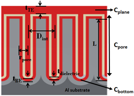
Figure 1. Schematic view of the cross section of the supercapacitor engineered onto the NAAM indicating the CDC layered structure and defining the lattice parameters involved in the capacitance calculation. Conductive layers of AZO are in red and dielectric layer of alumina in brown. Outlined are the 3 different contributions to total capacitance of the-designed supercapacitor prototype.
Both, the top (TE) and bottom (BE) electrodes material must exhibit good conductivity properties and the bottom electrode must have a low thickness (tBE) to achieve a remarkable increase in the capacitance values. For this reason, Al-doped ZnO (AZO) thin film is a great candidate to constitute the electrodes of the supercapacitor due to its attractive physical characteristics, such as excellent thermal stability and low electrical resistivity [29, 30]. The role played by dielectric materials is also relevant for the capacitor behavior, because the insulating material must have high dielectric constant and low thickness (tdielectric) to improve the capacitor capacitance (Equation 1), but if the thickness is too low, it will lead to the premature breakdown of the ESC. Alumina (Al2O3) is usually chosen as the insulating layer due to its ability for being deposited by ALD, its relatively high dielectric constant (k~7), exceptional stability and durability [31].
The total capacitance of the supercapacitor prototype designed on the basis explained above, could be calculated as the sum of the three different contributions to the whole capacitance, according to the supercapacitor geometry displayed in Figure 1, by including the planar space among pores (2), the cylindrical part of the pores (3), and finally the bottom of the pores (4) [17].
The contribution of the cylindrical part of pores is the major input to the total capacitance of the supercapacitor device given by formula (5), while the top electrode thickness (tTE) hardly influences the total capacitance of the supercapacitor, as it can be deduced from the Equations (2, 3, 4, and 5). Nevertheless, it needs to be thick enough to ensure good electrical contact and to protect the sample surface against external damage.
Herein, we discuss about the fabrication and development processes, together the morphological, structural and electrical study of a prototype of electrostatic supercapacitor. The prototype of the device follows the same principle as conventional electrostatic capacitors, but takes advantage of the high open surface area of nanoporous alumina membranes and the reduced thickness and elevated dielectric constant of the insulating layer deposited by ALD. The CDC structure of the ESC was formed by successively deposited layers on top-surface of a typical NAAM having pore diameter (Dp) about 65 nm, 105 nm of interpore distance (Dint) and pore length (L) around 10 μm. The conductor and dielectric alternating layers forming the CDC structure of the ESC were chosen of Aluminum-doped Zinc Oxide (AZO), as the BE and TE electrodes, with respective thicknesses of 12 and 24 nm, together with an intermediate insulating alumina (Al2O3) layer having a dielectric constant between 7–9 and 10 nm in thickness. This ESC prototype exhibits a high capacitance value about 200 μF/cm2 at the frequency of 40 Hz, and a breakdown voltage about 4–5 V, while the leakage current present values close to 1.8 mA/cm2 at 1 V. The high value of capacitance achieved in the supercapacitor prototype together with its small size makes these devices outstanding candidates for using in energy harvesting and storage applications.
Experimental
Fabrication of NAAM Templates
NAAM templates were fabricated starting from high-purity aluminum foil (99.999%, Goodfellow) with a thickness of 0.5 mm. Firstly, the sample was cleaned in isopropanol an ethanol. Then, the aluminum foils were electropolished in a two electrode electrochemical cell with a mixture of perchloric acid and ethanol (25:75 vol. %) at 5°C, under an applied voltaje of 20 V. The cathode was a Pt mesh counter electrode in the electrochemical cell and the aluminum foil was the anodic electrode. An alumina layer displaying a high aspect ratio honeycomb nanoporous structure was grown on top of the Al substrate, by following a well-known two step electrochemical anodization process in 0.3 M oxalic acid at a temperature between 1–3°C at 40 Vdc, (Figures 2A–D), as reported elsewhere [32].
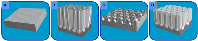
Figure 2. Schematic view of the two-step anodization process followed during the synthesis of a typical NAAM: (A) starting high purity Al foil; (B) random pores grown during the first anodization step; (C) chemical etching of the alumina layer; and (D) highly ordered porous alumina layer grown after second anodization step.
As a result, the NAAM template displays a highly spatial and periodically ordered distribution of the pores with hexagonal symmetry, having a pore diameter, Dp, about 35 nm, 105 nm of interdistance among nanopores, Dint, and pore length, L, around 10 μm, resulting in a pore density about 1 × 1010 cm−2 (Figure 3). Afterwards, the pores were widened by chemical etching in a weak dissolution of phosphoric acid (5 wt. %) during 35 min at 30°C, thus increasing Dp up to 65 nm. The pore widening aims to increase the pore size to contain the complete CDC structure constituting the electrostatic supercapacitor.
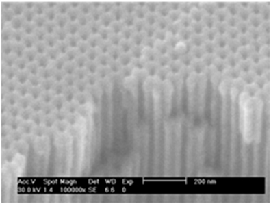
Figure 3. SEM image on top surface of a typical NAAM after the two-step anodization processes, where it can be appreciated the self-ordered porous structure with honeycomb arrangement, together a cross section break showing the parallel aligned longitudinal nanochannels.
Optimization of ALD Growth Rates of Conductive BE, TE, and Dielectric Layers
In order to determine the growth per cycle ratio of AZO and Al2O3 layers, different thicknesses of these oxides were deposited on Si substrates under the same deposition conditions that were used for NAAM substrates. Figures 4A,B) show the respective layer thicknesses measured using ellipsometry (black triangles) and profilometry (blue squares) techniques. The thickness exhibits a lineal behavior with the number of cycles. The growth per cycle (GPC) of the AZO and Al2O3 layers in ALD expo mode are 0.188 ± 0.002 nm/cycle and 0.127 ± 0.001 nm/cycle, respectively, which are comparable values with that reported in the literature for similar deposition conditions to here employed [31, 33].
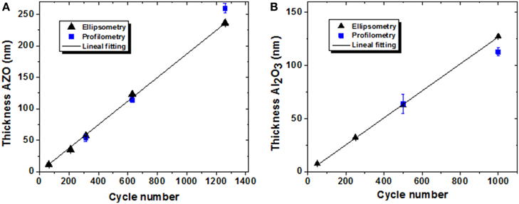
Figure 4. Thickness of different AZO (A), and Al2O3 (B), films deposited on Si substrates. The thicknesses were measured by using ellipsometry (black triangles) and profilometry (blue squares) techniques.
In this work, an Al doping ratio of 20:1 was chosen for the AZO films. Thus, the real concentration of Al follows the “rule of mixtures” at low dopant concentrations and it can be estimated through the expression:
Where n represents de number of ZnO cycles in the AZO supercycle. For the case of the AZO films with n = 20, the estimated %Al was 3.28%. This value of Al doping concentration can be considered the most appropriated according to other previous studies carried out to optimize the microstructure and therefore the electrical characteristics of the AZO films deposited by ALD, in order to obtain high degree of crystallinity, low resistivity and decrease in band gap of the conductive layer [33–35]. The measured resistivity of the AZO films was 1.5 × 10⁻⁴ Ω·cm, which is similar to the experimental values obtained in several reports [33, 34]. Higher Al contents in the AZO composition would increase the electrical resistivity due to the transformation of the conductor AZO film into insulator. In addition, it would also decrease the mobility and concentration of the charge carriers, thus reducing the electrical conduction properties of the AZO films [34].
CDC Layered Structure Deposited by ALD on Nanoporous Alumina Templates
The ESCs were prepared employing the ALD technique by coating the surface and inner pores of the starting NAAM template (Figure 5A) with a thin film of AZO as the bottom (Figure 5B) and top (Figure 5D) electrodes, respectively, and an Al2O3 layer as the intermediate dielectric (Figure 5C), as it is shown in the complete scheme displayed in the Figure 5.
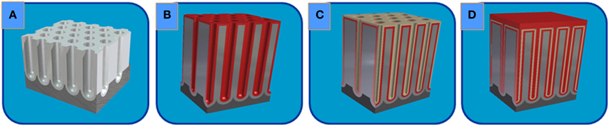
Figure 5. Schematic illustration of the CDC nanostructured layers deposited by ALD on nanoporous alumina templates for the ESC fabrication: (A) starting highly ordered nanoporous alumina template; (B) AZO Bottom Electrode conformally deposited by ALD; (C) intermediate Dielectric layer of Al2O3; and (D) after ALD deposition of the AZO Top Electrode.
The AZO and alumina thin layer depositions were performed in an ALD reactor (Savanah 100) at 200°C, using N2 as the carrier and purging gas, and operating in exposure mode. This operating mode provides slower deposition processes as compared to the flow mode, but it is particularly suitable for conformal depositions on surfaces with high aspect ratio, as in the case of NAAM templates [36]. Trimethyl aluminum (TMA) and H2O were used as precursors to deposit the Al2O3 layer at a deposition rate of 0.127 ± 0.001 nm per cycle to grow a thickness of 10.17 ± 0.07 nm dielectric layer. The AZO films were composed of alternate 20 cycles of ZnO and 1 cycle of Al2O3. The precursors utilized to deposit AZO were DEZ (diethyl zinc), TMA and H2O at a deposition rate of 0.188 ± 0.002 nm per cycle. This provided thicknesses of 11.9 ± 0.1 nm and 23.7 ± 0.3 nm for the BE and TE, respectively. The trilayer structure CDC reaches a thickness of 45 nm, but due to the cylindrical shape of the pore, it constitutes a total thickness of 90 nm, filling completely the nanopore diameter of NAAM template, as it is depicted in Figure 5D).
Electrical Contacts
The separated electrical contacts for the bottom and top electrodes were fabricated by masking a part of the supercapacitor after the first deposition of the bottom electrode with Kapton tape. Afterwards, the dielectric and top electrode layers were deposited and after the CDC structure was completely deposited, the mask was then removed, therefore exposing the bottom electrode. Later on, both the bottom and top electrodes were contacted using a conductive epoxy resin to make two electrical contacts by separately.
Microstructure and Electrical Characterization
Material characterization was carried out using a JEOL 6610 LV SEM (Scanning Electron Microscopy) and JEOL JEM 2100 TEM (Transmission Electron Microscopy), proving the deposition conformality and layer thicknesses. Structure and compositional characterizations were conducted using an X-Ray diffractometer and STEM (Scanning Transmission Electron Microscopy). Prior to TEM and STEM characterization, the NAAM coated with the CDC structure, was thinned by ion milling with Ar on the upper and lower sides of the nanocapacitor, employing a Gatan 691 Precission Ion Polishing System, operated at 3–5 kV. Resistivity measurements of conductor AZO films were performed with a four-point probe. Device capacitance and electrical impedance were measured with an Agilent 4294a LCR meter at frequencies ranging between 40 Hz and 100 MHz, and applying 500 mV (AC). Likewise, the leakage current and the breakdown voltage measurements were carried out by means of a homemade experimental setup consisting of a DC power supply model Keithley 2400 Source Meter, a variable resistor and the supercapacitor prototype, all together connected in series. For each leakage current measurement performed at any certain value of voltage, it has been waited long time enough (about 1 min) in order to ensure the stabilization of the leakage current value.
Results and Discussions
SEM images shown in Figure 6 summarize the top-view surface evolution of the pore diameter during the successive ALD depositions of conductive and dielectric layers of the CDC engineered structure that constitutes the electrostatic supercapacitor prototype, starting from the initial NAAM template displayed in Figure 6A). The first conductive thin layer was formed by 63 cycles of AZO as the BE (Figure 6B), followed by 80 Al2O3 cycles as the dielectric layer (Figure 6C), and finally 126 cycles of AZO as the TE (Figure 6D), which verified the correct deposition rates for the different CDC layers. Moreover, the thickness measured for the AZO layer at the BE was tBE = 10 ± 2 nm and the corresponding one for the Al2O3 dielectric layer was tdielectric = 8 ± 3 nm. These layer thicknesses values were in good agreement with the fitted ones estimated from the AZO and Al2O3 GPC.
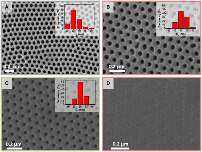
Figure 6. SEM top view images of NAAM templates showing the evolution of the pore diameter after successive ALD depositions for the supercapacitor prototype. (A) top view of the starting NAAM before the ALD process; (B) after deposition of 63 cycles of AZO as the BE; (C) top surface of nanopores after deposition of the BE and 80 cycles of Al2O3 dielectric layer; (D) SEM image after deposition of the complete CDC structure (63 cycles BE + 80 cycles dielectric layer + 126 cycles TE).
TEM top-view images displayed in Figures 7A,B), that were taken from samples after ion milling of the top and bottom sides of the CDC structure, confirmed the existence of three concentric layers with the expected spatial distribution and thicknesses near the values calculated from the GPC. The contrast differences in the images are due to the different density of both materials: AZO electrodes mainly composed of ZnO (density of 5.61 g·cm−3), and the Al2O3 in the NAAM and dielectric layer (density of 3.95 g·cm−3). Moreover, STEM mode image (Figure 7C) and compositional analysis profile (Figure 7D) confirm the existence of three concentric layers from the pore center: AZO top electrode, next to dielectric layer of Al2O3 and finally the layer of AZO constituting the bottom electrode. These experimental results evidence the CDC morphological structure of the engineered ESC, as schematically described in Figure 5.
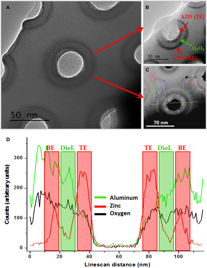
Figure 7. (A) TEM top view image of a planar section of the sample structure after being carefully prepared for displaying the nanopores after depositing the CDC structure. (B) TEM image showing the different CDC layers constituting the supercapacitor: BE and TE of AZO layers are represented in red color and the Al2O3 dielectric layer in green. (C) STEM image and (D) compositional analysis along the line-scan profile of the pore indicated in (C), where it is clearly evidenced the presence of three elements [zinc (blue), aluminum (red) and oxygen (green)], which spatially match with the CDC structure deposited on the NAAM.
By analyzing with more detail the inner part of the pores, the crystalline structure of the AZO top electrode can be evidenced in the HR-TEM analysis shown in Figure 8A). X-Ray diffraction analysis shown in Figure 8B), displays the diffraction peaks corresponding to aluminum substrate and zinc oxide. However, there are not peaks coming from the alumina due to its amorphous structure. Using the width of the zinc oxide peaks and the Scherrer equation [37], it is possible to calculate the grain size of AZO nanocrystals, obtaining a value of 5.6 ± 0.6 nm. This value is in agreement with the data extracted from the selected area electron diffraction spectra (SAED) and the high resolution TEM image displayed in Figure 8A). The AZO crystallinity is related with an enhancement of the electrical conductivity and improves the properties of capacitor electrodes.
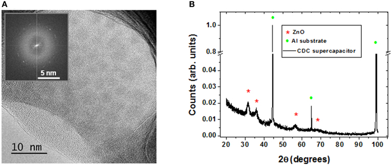
Figure 8. (A) TEM image of the inner pore shows the crystalline structure of AZO films, inset corresponds to the SAED (Select Area Electron Diffraction) analysis; (B) X-Ray diffraction pattern study of the supercapacitor device surface.
The impedance measurements shown in Figures 9A,B, display the module of impedance and phase behavior for the supercapacitor prototype and its comparison with a typical commercial capacitor, in the wide frequency range of 40 Hz up to 110 MHz. The impedance module decreases at low frequencies until it reaches the supercapacitor resonance frequency at about 2.5 MHz. When frequency increases, the module of the impedance rises up and the supercapacitor exhibits an inductive behavior at high frequencies. This is also the typical behavior of the impedance in a conventional capacitor, while the values for the module of the impedance and its resonance frequency are both lower than the corresponding ones compared with the supercapacitor prototype.
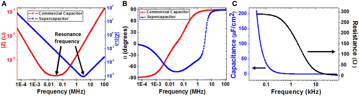
Figure 9. Electric characterization of the supercapacitor prototype and its comparison with a commercial capacitor: (A) impedance module, Z, and (B) phase, θ, in the frequency range of 40 Hz and 110 MHz. (C) Capacity and Resistance curves fitted according to a LCR circuit connected in series in the frequency range between 40 Hz and 70 kHz, for the supercapacitor device.
On the other part, negative values for the phase of the impedance are reached at frequencies below that of the supercapacitor resonance, while at frequencies close to 40 Hz the phase of the impedance takes anomalous negative values, but that does not reach −90°, as it would be expected for a conventional capacitor, also displayed in the Figure 9B. Nevertheless, for frequencies higher than the resonance frequency, the impedance phase increases reaching positive values, which is characteristic of an inductive behavior. The unusual phase performance at low frequencies could be due to a high device leakage current (Figure 10A), which provokes a strong resistive contribution in the supercapacitor prototype behavior at frequencies near 40 Hz.
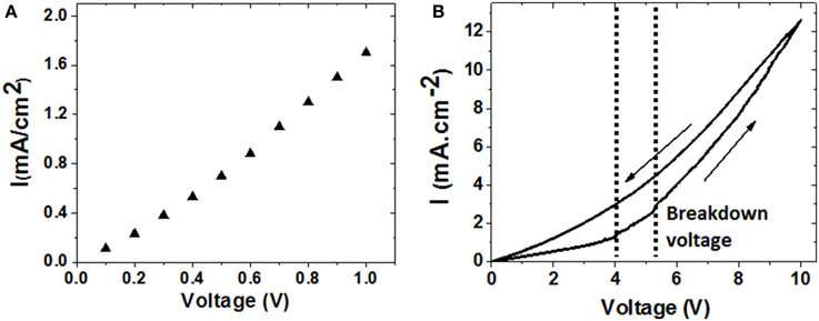
Figure 10. I–V curves characteristic of the CDC supercapacitor. (A) Leakage current measurement in the low voltage range of 0–1 V; (B) cycling performance indicating the breakdown voltage of the ESC prototype.
Additionally, the frequency variation of the capacitance of the device, which is shown in Figure 9C, has been estimated with the LCR meter by modeling the supercapacitor behavior with an equivalent circuit composed by a capacitor, a resistance and an inductance all together connected in series. This basic equivalent circuit is commonly used to represent the performance of the conventional capacitors. Maximum capacitance value about 200 μF/cm2 is reached at the frequency of 40 Hz, which decreases drastically when the measurement frequency is increased. This property indicates that the future device applications should be focus on the low frequency range where the supercapacitor prototype exhibits the largest electrical energy storage properties. Furthermore, by using the Equations (2–5), it is also possible to calculate a theoretical value of the device capacitance, by introducing the morphologic parameters of the studied ESC prototype (rpore = 65 nm; Dint = 105 nm; L = 10 μm; α = 1 × 1010 cm−2; tBE = 11.9 nm; tdielectric = 10.17 nm). The estimated calculation of the capacitance gives a result of 201 ± 20 μF/cm2, which is in good agreement with the capacitance value obtained from the LCR approach.
In spite of that, the anomalous phase behavior displayed by the impedance at low frequencies, together the high resistance value obtained, suggests that the LCR equivalent circuit chosen to represent the behavior of the supercapacitor prototype may not be the most appropriate for modeling the impedance response of the supercapacitor device in this frequency range. Due to the complex engineered structure of the device/sample, the impedance behavior of the prototype should be adjusted with another more complicated model of equivalent circuit composed of serial and/or parallel associations of resistors and capacitors, as those reported in the literature for other similar prototypes of supercapacitor devices [38–40].
Leakage current of the supercapacitor device was measured for different applied voltages, obtaining a linear behavior with high leakage current values of 1.7 mA/cm2 at voltages up to 1 V, as it can be seen in Figure 10A). The obtained leakage current values are high, which may be a handicap for applications of this ESC prototype in long-term energy storage applications. The origin of such high leakage current values could be due to the existence of local defects in the CDC structure, or chemical impurities that increase the conductivity of the dielectric alumina layer, as well as the strong electric field localized at the sharp tips of the membrane surface. However, different strategies can be further explored to improve this feature of the ESC prototype, such as by increasing the thickness and uniformity of the dielectric layer, by introducing a passivation layer or an anodic alumina barrier to soften the NAAM profile and get avoided the electrical losses due to the sharp tips on the membrane surface [12, 18].
Finally, the characteristic current-voltage curve (I–V) shows a breakdown voltage about 5 V, as it can be shown in Figure 10B. On the upwards curve slope of the characteristic I–V representation, it is noticed that the current increases forcefully at this value of voltage, indicating the completely dielectric breakdown in the device. However, in the marked area between the two discontinuous bars, it is possible to appreciate that the dielectric breakdown is not abrupt, but it seems to take place gradually by breaking different parts of the dielectric layer as the voltage is continuously increased, which is consistent with the parallel arrangement of individual nano-capacitors embedded in the NAAM template. Nevertheless, on the slope of the descending curve it can be observed a higher current flow through the supercapacitor prototype as compared with the upward curve, clearly indicating the dielectric breakdown and hence, an irreversible damage in the supercapacitor prototype ability for storing the electrical energy.
Conclusions
In summary, we report on the fabrication and characterization of ESCs by ALD conformal deposition of a CDC engineered structure on the high open surface of a NAAM as template. The excellent conformality of both deposited conductive and dielectric layers, together with their composition and crystalline structure have been checked by means of different XRD and electron microscopy techniques. The complete electric characterization was carried out in the frequency range of 40 Hz up to 100 MHz by using a LCR impedance analyzer. It is found that the capacitance per unit area decreases strongly with the frequency, but at the low frequency of 40 Hz it reaches about 200 μF/cm2. This result is well correlated with the theoretically calculated capacitance according with the geometric structure of the ESC prototype. Additionally, the frequency dependence of the impedance module and phase indicate that ENCs follow a frequency behavior similar to commercial capacitors, but showing enhanced capacitance areal density. This comprehensive study is particularly interesting because the electrostatic capacitors can usually exhibit higher power densities than compared to batteries, but their capacitive properties do not degrade over the time such as the electrolytic capacitors. Looking forward it becomes necessary to improve the features of the ESC prototype device in order to minimize the leakage current and breakdown voltage, thus optimizing the impedance behavior and power density of the supercapacitor, but without sacrificing the energy storage density of the device.
Conflict of Interest Statement
The authors declare that the research was conducted in the absence of any commercial or financial relationships that could be construed as a potential conflict of interest.
Acknowledgments
This work has been financially supported under Spanish research projects MICINN MAT2010-20798-C05-04, together MINECO MAT2013-48054-C2-2-R and MAT2013-47231-C2-1-P. JG acknowledges to FICYT for his “Severo Ochoa” fellowship. Scientific support from the University of Oviedo SCT's, particularly to the Laboratorio de Membranas Nanoporosas at Nanotechnology Unit, is also recognized.
References
1. Burke A. Ultracapacitors: why, how, and where is the technology. J Power Sources. (2000) 91:37. doi: 10.1016/S0378-7753(00)00485-7
2. Yan J, Wang Q, Wei T, Fan Z. Recent advances in design and fabrication of electrochemical supercapacitors with high energy densities. Adv Energy Mater. (2014) 4:1300816. doi: 10.1002/aenm.201300816
3. Kondrat S, Pérez CR, Presser V, Gogotsi Y, Kornyshev AA. Effect of pore size and its dispersity on the energy storage in nanoporous supercapacitors. Energy Environ Sci. (2012) 5:6474–9. doi: 10.1039/c2ee03092f
4. Kondrat S, Kornyshev A. Charging dynamics and optimization of nanoporous supercapacitors. J Phys Chem C. (2013) 117:12399–406. doi: 10.1021/jp400558y
5. Lee AA, Kondrat S, Oshanin G, Kornyshev AA. Charging dynamics of supercapacitors with narrow cylindrical nanopores. Nanotechnology (2014) 25:315401. doi: 10.1088/0957-4484/25/31/315401
PubMed Abstract | Full Text | CrossRef Full Text | Google Scholar
6. Kondrat S, Kornyshev A, Stoeckli F, Centeno TA. The effect of dielectric permittivity on the capacitance of nanoporous electrodes. Electrochem Comm. (2013) 34:348–50. doi: 10.1016/j.elecom.2013.07.009
7. Zhou H, Zhang Y. Electrochemically self-doped TiO2 nanotube arrays for supercapacitors. J Phys Chem C. (2014) 118:5626–36. doi: 10.1021/jp4082883
8. Aricò AS, Bruce P, Scrosati B, Tarascon JM, van Schalkwijk W. Nanostructured materials for advanced energy conversion and storage devices. Nat Mater. (2005) 4:366. doi: 10.1038/nmat1368
PubMed Abstract | Full Text | CrossRef Full Text | Google Scholar
9. Wang K, Wang Y, Wang Y, Hosono E, Zhou, H. Mesoporous carbon nanofibers for supercapacitor application. J Phys Chem C. (2009) 113:1093–7. doi: 10.1021/jp807463u
10. Liu C, Li F, Ma LP, Cheng, HM. Advanced materials for energy storage. Adv Mater. (2010) 22:E28. doi: 10.1002/adma.200903328
PubMed Abstract | Full Text | CrossRef Full Text | Google Scholar
11. Vellacheri R, Al-Haddad A, Zhao H, Wang W, Wang C, Lei Y. High performance supercapacitor for efficient energy storage under extreme environmental temperatures. Nano Energy (2014) 8:231. doi: 10.1016/j.nanoen.2014.06.015
12. Bufon CCB, González JDC, Thurmer DJ, Grimm D, Bauer M, Schmidt GO. Self-assembled ultra-compact energy storage elements based on hybrid nanomembranes. Nano Lett. (2010) 10:2506. doi: 10.1021/nl1010367
PubMed Abstract | Full Text | CrossRef Full Text | Google Scholar
13. Yu G, Xie X, Pan L, Bao Z, Cui Y. Hybrid nanostructured materials for high-performance electrochemical capacitors. Nano Energy (2013) 2:213. doi: 10.1016/j.nanoen.2012.10.006
14. Chen X, Li C, Grätzel M, Kostecki R, Mao SS. Nanomaterials for renewable energy production and storage. Chem Soc Rev. (2012) 41:7909. doi: 10.1039/c2cs35230c
PubMed Abstract | Full Text | CrossRef Full Text | Google Scholar
15. Grote F, Lei Y. A complete three-dimensionally nanostructured asymmetric supercapacitor with high operating voltage window based on PPy and MnO2. Nano Energy (2014) 10:63. doi: 10.1016/j.nanoen.2014.08.019
16. Yota J, Shen H, Ramanathan R. Characterization of atomic layer deposition HfO2, Al2O3, and plasma enhanced chemical vapor deposition Si3N4 as metal–insulator–metal capacitor dielectric for GaAs HBT technology. J Vac Sci Technol A. (2013) 31:01A134. doi: 10.1116/1.4769207
17. Banerjee P, Pérez I, Henn-Lecordier L, Lee SB, Rubloff GW. Nanotubular metal–insulator–metal capacitor arrays for energy storage. Nat Nanotechnol. (2009) 4:292. doi: 10.1038/nnano.2009.37
PubMed Abstract | Full Text | CrossRef Full Text | Google Scholar
18. Haspert LC, Lee SB, Rubloff GW. Nanoengineering strategies for metal–insulator–metal electrostatic nanocapacitors. ACS Nano (2012) 6:3528. doi: 10.1021/nn300553r
PubMed Abstract | Full Text | CrossRef Full Text | Google Scholar
19. Li LJ, Zhu B, Ding SJ, Lu HL, Sun HL, Sun QQ, et al. Three-dimensional AlZnO/Al2O3/AlZnO nanocapacitor arrays on Si substrate for energy storage. Nanoscale Res Lett. (2012) 7:544. doi: 10.1186/1556-276X-7-544
PubMed Abstract | Full Text | CrossRef Full Text | Google Scholar
20. Shelimov KB, Davydov DN, Moskovits M. Template-grown high- density nanocapacitor arrays. Appl Phys Lett. (2000) 77:1722. doi: 10.1063/1.1290598
PubMed Abstract | Full Text | CrossRef Full Text | Google Scholar
21. Hourdakis E, Nassiopoulou AG. High performance MIM capacitor using anodic alumina dielectric. Microelectron Eng. (2012) 90:12. doi: 10.1016/j.mee.2011.03.020
22. Prida VM, Sanz R, Vega V, Navas D, Pirota KR, Asenjo A, et al. Self-assembled nanoporous oxide membranes. Encyclopedia Nanosci Nanotechnol. (2011) 22:509.
23. Jani AMM, Losic D, Voelcker, NH. Nanoporous anodic aluminium oxide: advances in surface engineering and emerging applications. Prog Mater Sci. (2013) 58:636. doi: 10.1016/j.pmatsci.2013.01.002
24. Lin CC, Yang CL. Carbon nanotubes grown on nanoporous alumina templates/aluminum foil for electrodes of aluminum electrolytic capacitors. J Electrochem Soc. (2010) 157:A237. doi: 10.1149/1.3272640
25. Aguilera A, Jayaraman V, Sanagapalli S, Singh RS, Jayaraman V, Sampson K, et al. Porous alumina templates and nanostructured CdS for thin film solar cell applications. Solar Energ Mater Solar Cells. (2006) 90:713. doi: 10.1016/j.solmat.2005.04.008
26. George SM. Atomic layer deposition: an overview. Chem Rev. (2010) 110:111. doi: 10.1021/cr900056b
PubMed Abstract | Full Text | CrossRef Full Text | Google Scholar
27. Knez M, Nielsch K, Niinistö L. Synthesis and surface engineering of complex nanostructures by atomic layer deposition. Adv Mater. (2007) 19:3425. doi: 10.1002/adma.200700079
28. Leskelä M, Ritala M. Atomic layer deposition (ALD): from precursors to thin film structures. Thin Solid Films (2002) 409:138. doi: 10.1016/S0040-6090(02)00117-7
29. Geng Y, Guo L, Xu S-S, Sun Q-Q, Ding S-J, Lu H-L, et al. Influence of Al doping on the properties of ZnO thin films grown by atomic layer deposition. J Phys Chem C. (2011) 115:12317–21. doi: 10.1021/jp2023567
30. Elam JW, Routkevitch D, George SM. Properties of ZnO/Al2O3 alloy films grown using atomic layer deposition techniques. J Electrochem Soc. (2003) 150:G339. doi: 10.1149/1.1569481
31. Herrmann, CF, DelRio FW, George SM, Bright VM. Properties of atomic layer deposited Al2O3/ZnO dielectric films grown at low-temperature for RF MEMS. Micromach Microfabr Process Technol X. (2005) 5715:159. doi: 10.1117/12.589322
32. Masuda H, Fukuda K. Ordered metal nanohole arrays made by a two-step replication of honeycomb structures of anodic alumina. Science (1995) 268:1466. doi: 10.1126/science.268.5216.1466
PubMed Abstract | Full Text | CrossRef Full Text | Google Scholar
33. Hou Q, Meng F, Sun J. Electrical and optical properties of Al-doped ZnO and ZnAl2O4 films prepared by atomic layer deposition. Nanoscale Res Lett. (2013) 8:144. doi: 10.1186/1556-276X-8-144
PubMed Abstract | Full Text | CrossRef Full Text | Google Scholar
34. Banerjee P, Lee WJ, Bae KR, Lee SB, Rubloff GW. Structural, electrical, and optical properties of atomic layer deposition Al-doped ZnO films. J Appl Phys. (2010) 108:043504. doi: 10.1063/1.3466987
35. Lee DJ, Kim HM, Kwon JY, Choi H, Kim SH, Kim KB. Structural and electrical properties of atomic layer deposited Al-doped ZnO films. Adv Funct Mater. (2011) 21:448. doi: 10.1002/adfm.201001342
36. Elam JW, Routkevitch D, Mardilovich PP, George SM. Conformal coating on ultrahigh-aspect-ratio nanopores of anodic alumina by atomic layer deposition. Chem Mater. (2003) 15:3507. doi: 10.1021/cm0303080
37. Scherrer P. Bestimmung der Gröse und der inneren Struktur von Kolloidteilchen mittels Röntgenstrahlen. Nachr Ges Wiss Göttingen. (1918) 26:98
38. Fisher RA, Watt MR, Ready WJ. Functionalized carbon nanotube supercapacitor electrodes: a review on pseudocapacitive materials. ECS J Solid State Sci Technol. (2013) 2:M3170. doi: 10.1149/2.017310jss
39. Devillers N, Jemei S, Pèra MC, Bienaimé D, Gustin F. Review of characterization methods for supercapacitor modelling. J Power Sources. (2014) 246:596. doi: 10.1016/j.jpowsour.2013.07.116
Keywords: supercapacitor, nanoporous alumina membranes, atomic layer deposition, leakage current, energy storage, energy harvesting
Citation: Iglesias L, Vega V, García J, Hernando B and Prida VM (2015) Development of electrostatic supercapacitors by atomic layer deposition on nanoporous anodic aluminum oxides for energy harvesting applications. Front. Phys. 3:12. doi: 10.3389/fphy.2015.00012
Received: 17 January 2015; Paper pending published: 03 February 2015;
Accepted: 25 February 2015; Published: 25 March 2015.
Edited by:
Zorica Konstantinovic, Institut de Ciència de Materials de Barcelona - CSIC, SpainReviewed by:
Alberto Pomar, Institut de Ciència de Materials de Barcelona - CSIC, SpainJulian M. Gonzalez, University of the Basque Country, Spain
Copyright © 2015 Iglesias, Vega, García, Hernando and Prida. This is an open-access article distributed under the terms of the Creative Commons Attribution License (CC BY). The use, distribution or reproduction in other forums is permitted, provided the original author(s) or licensor are credited and that the original publication in this journal is cited, in accordance with accepted academic practice. No use, distribution or reproduction is permitted which does not comply with these terms.
*Correspondence: Víctor M. Prida, Departamento de Física, Facultad de Ciencias, Universidad de Oviedo, Calvo Sotelo s/n, 33007-Oviedo, Asturias, Spain vmpp@uniovi.es