Silicon photonic integration in telecommunications
 Christopher R. Doerr
- Acacia Communications, Hazlet, NJ, USA
Silicon photonics is the guiding of light in a planar arrangement of silicon-based materials to perform various functions. We focus here on the use of silicon photonics to create transmitters and receivers for fiber-optic telecommunications. As the need to squeeze more transmission into a given bandwidth, a given footprint, at a given cost increases, silicon photonics makes more and more economic sense.
1. Introduction
Until circa 2002, fiber-optic communication for metropolitan distances (80—600 km) and long-haul distances (600–15,000 km) employed mostly simple on-off keying (OOK) transmission. On-off keying is simply turning on and off the light to transmit “1” s and “0” s. Higher performance, i.e., a lower bit-error rate (BER) for the same received optical power and/or for the same optical signal-to-noise ratio (OSNR), can be obtained by using phase-modulated formats, such as binary phase-shift keying (BPSK) or quadrature phase-shift keying (QPSK). They maximize the distance between constellation points for the same average signal power. In these “advanced” modulation formats [1], the term “symbol” is used to represent each data portion in time, because each symbol can carry multiple bits of information. Early BSPK and QPSK were detected by differential detection, i.e., by interfering one symbol with the previous symbol in an interferometer in the receiver.
However, bandwidth needs have been constantly growing exponentially. It is expensive to install new optical fibers, ~$30 k per mile [2], so carriers and data-center operators needed to send more bits per second in the same fiber in the same optical bandwidth. One key way is to use both optical polarizations, because this doubles the available bandwidth. Although signal orthogonality is maintained, their polarizations are essentially randomly changed during propagation through fiber. To unscramble them requires significant signal processing. Optical coherent detection allows this to be done by digital electronics.
Optical coherent detection was a hot topic in the 1980s, because it is a form of optical amplification. However, the invention of the erbium-doped fiber amplifier (EDFA) eliminated that advantage and coherent interest died away. Another advantage of coherent detection is the ability to receive the full optical field, both the real and imaginary parts of both polarizations. With improvements in complementary metal-oxide-semiconductor (CMOS) electronics, digital signal processing (DSP) became available circa 2002 to handle coherent detection even up to 100-Gb/s, causing a revival of coherent detection. In the past, coherent detection was simply single quadrature and single polarization. Now it is dual quadrature and dual polarization.
100-Gb/s coherent systems have proven to be extremely compelling. They allow an upgrade of a 10-Gb/s channel to a 100-Gb/s channel with actually improved reach. Industry analyses show the number of metro and long-haul 100-Gb/s coherent transceivers sold per year to be on a steep upwards ramp as 10-Gb/s OOK transceivers are replaced by 100-Gb/s coherent transceivers.
However, the price of 100-Gb/s coherent transceivers is expected to drop significantly. This is because users want to pay the same price per connection even though the bit rate keeps increasing. However, not only must the price drop, but the footprint and power consumption as well. As seen in Figure 1, 100-Gb/s modules have gone from full line cards to 5 × 7 in2 screwed-on modules to 3.2 × 5.7 in2 pluggable modules today. Today's 100-Gb/s pluggable form factor is called a CFP. Tomorrow's will be a CFP2, which is half the size, and eventually a CFP4, which is a quarter the size. Power consumptions have gone from more than 100 W on a line card, to 70 W for the screwed-on module, to 28 W for the CFP. The next step, the CFP2, allows only 12W.
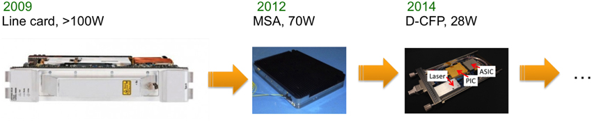
Figure 1. 100-Gb/s coherent transceiver form-factor evolution. It went from a full line card, to a multi-source agreement (MSA) module, to a 100-Gb/s form-factor pluggable (CFP) module. The D in D-CFP means that it is a digital module and the DSP is included inside, as opposed to a module that contains only the optics.
There are two main components in a coherent transceiver—the DSP chip and the optics. Today's coherent CFP contains both. There is a, possibly temporary, trend to take the DSP out of the module and put it on the line card. Such modules are called “analog” modules, rather than digital. With today's technology, it is not possible to have both the optics and DSP be under 12 W, the maximum power in a CFP2. However, in 1–2 years, technology will likely be ready for a “digital” CFP2.
To meet these requirements of lower price, lower power and smaller footprint, one must make advancements in technology. For the DSP, one can take advantage of the steady reduction in transistor size in industry, which reduces power and footprint. Node size and introduction year are shown in Table 1 [3]. Today's coherent DSPs use 20–28 nm. Tomorrow's will use 14 nm.
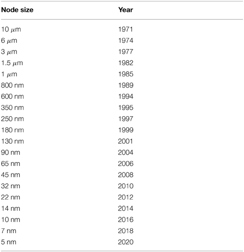
Table 1. Node size and first year of commercial introduction for CMOS electronics.
For the optics, one must use photonic integration, the focus of this article. Most of today's coherent transceivers are built using separate LiNbO3/planar lightwave circuit (PLC) modulators and InP/PLC receivers, as shown in Figure 2. More and more, smaller InP modulators and InP receivers are being used. In today's coherent CFP, there is a single silicon photonic (SiPh) integrated circuit (PIC) containing both the transmitter and receiver [4]. Not shown is a separate tunable laser.
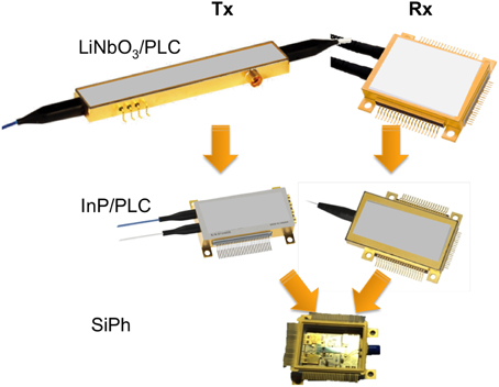
Figure 2. 100-Gb/s coherent optics evolution, going from LiNbO3 modulators and planar lightwave circuit (PLC)-based receivers to InP-based modulators and receivers to silicon photonic modulators and receivers.
Finally, a dominant cost for the DSP and optics is the packaging; one can further reduce cost, power, and footprint by co-packaging the DSP and optics. Such transceivers are expected in 2–3 years.
Figure 3 shows many of the elements that may be integrated in a PIC. The blue are passive, the red are active (have an intended dynamic interaction between light and matter), and the green are electronic components. PICs have been around more than 20 years. The main advantages of photonic integration are a small footprint, due to strongly confining waveguides and lens-free connections between parts; low power, due to an obviation of 50-Ω RF lines; higher bandwidth RF connections; and low price, due to fewer touch points, no mechanical adjustments, less test equipment, and less material. The main disadvantages of PICs are typically a higher insertion loss and the inability to optimize components independently.
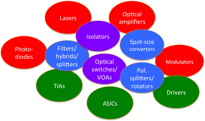
Figure 3. Some of the possible PIC integration elements.
2. PIC Material Systems
Figure 4 shows the most popular PIC material systems. From left to right there are silica-on-silicon PICs, also called PLCs; silicon-on-insulator PICs, also called silicon photonics; lithium niobite (LiNbO3); and III–V PICs, such as InP and GaAs. This article focuses on silicon photonics. In silicon photonics, the light is mostly guided in silicon, which has an indirect bandgap of 1.12 eV (1.1 μm). The silicon is a pure crystal grown in a boule and then sliced into wafers, today typically 300 mm in diameter, as shown in Figure 5. The surfaces are oxidized to form SiO2 layers. One wafer is bombarded with hydrogen atoms to a specified depth. Then the two wafers are placed together in a vacuum, and the oxide layers bond to each other. The assembly is cracked at the hydrogen implantation line. Then the silicon layer where the crack was is polished, and one is left with a thin layer of crystalline silicon on a layer of oxide on a full silicon “handle” wafer. The waveguides are formed from this thin crystalline layer. While these silicon-on-insulator (SOI) wafers are what makes low-loss silicon photonic waveguides possible, they are actually used mostly for low-power CMOS circuits, because of the low leakage currents they offer.
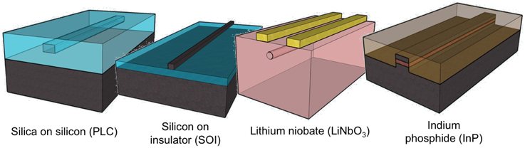
Figure 4. Popular PIC material systems. The second from the left is a silicon wire waveguide and is the focus of this article.
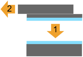
Figure 5. How a silicon-on-insulator (SOI) wafer is made. Each wafer is made from two silicon wafers. The wafers are oxidized, bonded, and one is cut and polished to a thin layer.
There is a wide family of possible silicon-based optical waveguides, shown in Figure 6. They range from micro-scale Ge-doped SiO2 waveguides to nano-scale Si wire waveguides. By adding Ge, one can make photodetectors and electro-absorption modulators. Potentially even optical amplifiers. By doping the silicon one can make optical modulators. From left to right at the bottom are silicon wire waveguides, silicon nitride waveguides, silicon oxynitride waveguides, thick silicon rib waveguides, thin silicon nitride waveguides, and doped silica waveguides. From left to right at the top are a depletion modulator, a Ge photodetector, and a Ge optical amplifier.
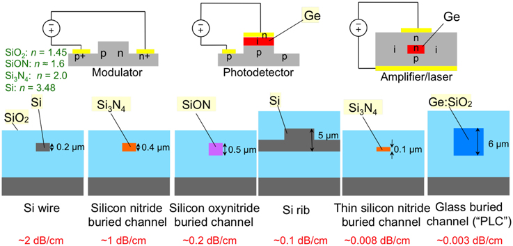
Figure 6. Cross sections of the family of Si-based optical waveguides. Also shown are typical propagation losses and refractive indices.
3. Si Photonic Passive Elements
There are several key silicon photonic passive elements. One is the surface-emitting grating coupler, as shown in Figure 7A [5, 6]. It consists of a strong grating in the waveguide with a pitch approximately equal to the wavelength in the waveguide. This causes light to emit or be received vertical to the surface, which is well-suited for wafer level measurements and/or coupling to an optical fiber. The grating coupler is somewhat unique to silicon photonics because it requires a high vertical index contrast. For example, if one tried to do a grating coupler in traditional InP waveguides, the light would simply leak away into the substrate rather than be emitted vertically, because the average index of the grating waveguide would be below that of the substrate. To make it work in InP, one must undercut the material under the grating, suspending it, as shown in Figure 7B [7].
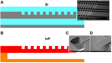
Figure 7. Surface-emitting 1-D grating couplers in silicon (A) and InP (B). In (A), the gray and light blue represent silicon and silicon dioxide, respectively. In (B), the red and orange represent InGaAsP and InP, respectively. (C,D) SEM pictures of the InP suspended cantilever grating coupler.
Another key element is a spot-size converter, which converts the ~ 0.5 × 1 μm2 mode of a Si wire waveguide to the ~ 10 × 10 μm2 mode of an optical fiber. A typical method is to use an inverse taper, in which the waveguide is narrowed down to a small tip, causing the optical mode to expand very large [8]. The mode can be captured by a suspended glass waveguide, such as in Figure 8 [9]. Coupling losses less than 1.5 dB are readily achievable with such spot-size converters.
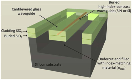
Figure 8. Spot-size converter for silicon wire waveguides. The silicon is inverse tapered inside a suspended glass waveguide. The silicon substrate has been etched away under the suspended glass waveguide.
Another key passive element is a polarization splitter. Some polarization splitter examples are shown in Figure 9. The first is a Mach-Zender interferometer with a different birefringence in each arm [10]. The second is a simple directional coupler [11]. The shape birefringence is so high in typical silicon wire waveguides, that the transverse-magnetic (TM) polarization can couple fully while the transverse-electric (TE) polarization has barely begun to couple. The third is a grating coupler in which the fiber is placed at an angle such that TE couples in one direction and TM the other [12]. The fourth is a 2D grating coupler [13]. The fiber mode with its electric field perpendicular to the waveguide propagation direction will couple to that waveguide. The fiber can be either tilted and couple to two waveguides or be normal to the surface and couple to four waveguides. The 2D grating coupler has the added advantage of acting as a polarization rotator, in that all the light on the chip has the same polarization yet was two orthogonal polarizations in the fiber.
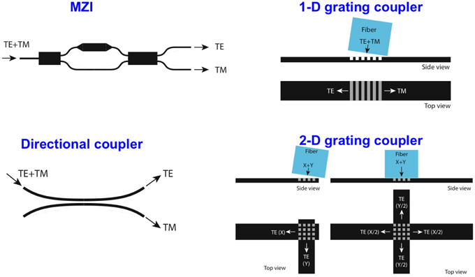
Figure 9. Various polarization splitters.
4. Si Photonic Active Elements
As mentioned above, a photonic active element has an intentional dynamic interaction between light and matter. A typical photonic active element is an optical modulator. All the Si optical modulators today are based on the plasma free carrier effect. The complex refractive index of the silicon changes by changing the number of free electrons and holes, either by doping, electrical means, or optical means, as shown in Equations (freecarrier_real, freecarrier_imag), obtained by fitting to data in Soref and Bennett at 1550-nm wavelength [14]. The holes have a larger ratio of real to imaginary index change, i.e., more phase change for a given loss change, and thus are usually favored for making the phase modulators in Mach-Zehnder and ring modulators.
Various Si modulator types are shown in Figure 10A. In the carrier injection modulator, the light is in intrinsic silicon inside a very wide p-i-n junction, and electrons and holes are injected. Such a modulator is slow, however, typically 500-MHz bandwidth, because it takes a long time for the free electrons and holes to recombine after injection. Thus, such structures are usually used as variable optical attenuators (VOAs) rather than modulators [15, 16]. In the carrier depletion modulator, the light is partly in a narrow p-n junction, and the depletion width of the p-n junction is varied by an applied electric field. Such a modulator can operate at over 50 Gb/s [17], but has a high background insertion loss. A typical VπL is 2 V-cm. The metal-oxide-semiconductor (MOS) (really semiconductor-oxide-semiconductor) modulator contains a thin oxide layer in the p-n junction [18]. It allows for some carrier accumulation as well as carrier depletion, allowing for a smaller VπL of ~0.2 V-cm, but with the drawbacks of higher optical loss and higher capacitance per unit length. There are also SiGe electroabsorption modulators [19] that rely on band-edge movement in SiGe. There are also graphene modulators that rely on switching the graphene between an absorbing metal and a transparent insulator [20].
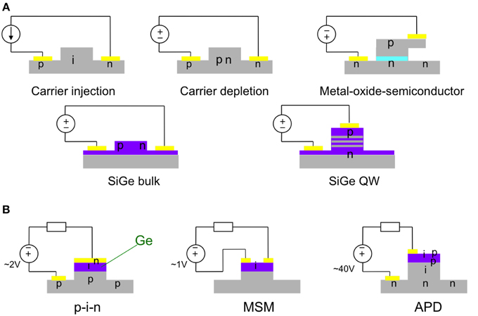
Figure 10. (A) Cross sections of various silicon-based optical modulator designs and (B) photodetector designs.
Various Si-based photodetectors are shown in Figure 10B. The absorption material is Ge. Ge absorbs light with wavelengths up to about 1.6 μm. Shown on the left is a p-i-n configuration [21], the most successful commercially today. It consists of p-doped silicon on which Ge is grown. Ge and Si have a 4% lattice mismatch, so to minimize dislocations, a thin layer of SiGe is grown first. The top of the Ge is n doped. Shown in the middle is a metal-semiconductor-metal (MSM) photodiode [22] and at the right avalanche photodiodes (APDs) [23]. The APD avalanche region is in Si, which has a lower noise than avalanche regions in III–V materials.
There is still no clear-winning solution for integrating optical gain with silicon photonics. Some of the various option are shown in Figure 11, organized by assembly level. On the far left is monolithic integration, including using epitaxially grown Ge as an optical gain material [24], Er-doped glass waveguides, such as Al2O3, (which require optical pumping) [25], and epitaxially grown GaAs quantum dots [26]. The next column is wafer-to-wafer assembly, including oxide bonding [27] and organic bonding [28] of III–V gain regions. The next column is die-to-wafer assembly, including inserting III–V die into cavities in the Si wafer and then patterning the waveguides [29]. The advantages of all the left three columns is that the full device can be tested on the wafer level, before it is diced out. The far right column is die-to-die assembly, including butt coupling of a Si die and a III–V die and coupling with a lens and a grating coupler [30]. Commercial deployment is tending to move from the right to left of this figure.
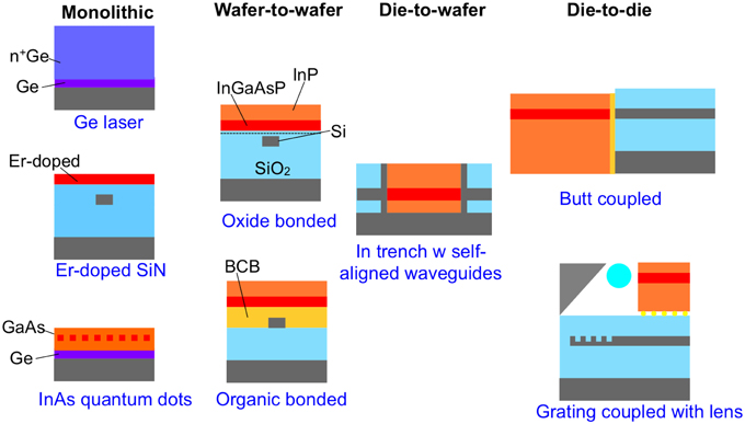
Figure 11. Configurations for integrating optical gain into silicon photonics. Fabrication insertion point becoming later in the process as one moves from left to right.
An element that is partway between an active and passive element is an optical isolator. Optical isolators are required to stop back reflections from causing noise and oscillations in lasers and optical amplifiers. An isolator requires a non-reciprocal element [31]. In silicon photonics, two main types of isolators have been reported: magneto-optic and modulation-based. In magneto-optic isolators, garnets are placed on the side or top of the waveguide [32, 33]. In a modulation-based isolator, the optical field is modulated with either a traveling wave or a time delay between multiple modulators [34]. Figure 12 shows a modulation-based isolator design based on a parallel arrangement of phase modulators in series [35]. Each modulator is driven by a sine wave. In the forward direction, the second modulator in each arm undoes the modulation of the first modulator; but in the backward direction, the two modulators add constructively. Thus, there is no effect at all on the signal in the forward direction but in the backward direction it is strongly phase modulated. If the phase modulation amplitude is just right, then a continuous-wave signal passing backwards is completely attenuated at its original frequency. This gives narrow-band isolation. By having multiple such narrow-band isolators in parallel, driven by the same frequency but appropriate different RF drive phases in each arm, one can achieve broadband isolation. A two-arm version was demonstrated in silicon photonics, achieving ~3 dB of isolation. The modulation was done by carrier injection in the silicon waveguide. The isolation can be improved by reducing the residual amplitude modulation in the phase modulators, by increasing the speed of the modulators, and/or by increasing the number of arms in the interferometer.
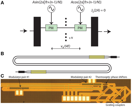
Figure 12. (A) configuration of an optical isolator that uses a tandem arrangement of phase shifters. There are N arms in the interferometer. The more the arms, the higher the broadband isolation. (B,C) 2-arm version built in silicon photonics.
5. PIC Material System Comparison
Table 2 shows a comparison between InP and Si. InP is a much more expensive material than Si because of the rarity of In. Si circuits tend to have a higher yield than InP circuits because there is much less epitaxy involved in Si circuits. In Si circuits, usually the only epitaxy is Ge, used in the photodetectors, whereas in InP all of the waveguides, even the passive ones, must be grown by epitaxy. Epitaxy tends to have a higher defect density than crystal growth from a boule. InP waveguides have high index contrast only laterally, whereas Si waveguides have high index contrast laterally and vertically. This allows much smaller bend radii and other more compact structures in Si. InGaAsP has a direct bandgap, whereas Si and Ge do not. Thus, the InP material system has a much more efficient laser. The native oxide of the InP system is much less robust than the native oxide of Si, which is SiO2. Silicon is a stronger material than InP, allowing for much larger wafers, 75 mm compared to 300 mm (going to 450 mm soon). InP modulators usually depend on the quantum-confined Stark effect, which is temperature sensitive because of the band edge movement with temperature. Silicon modulators have very minimal temperature dependence.
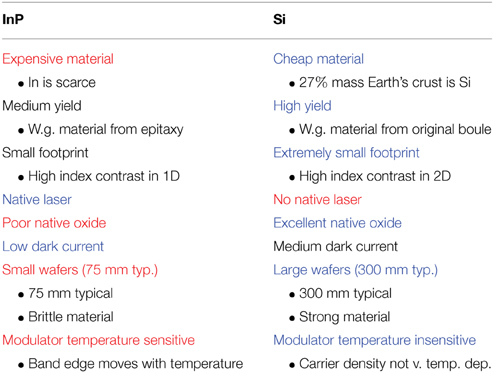
Table 2. Pros and cons of InP and Si for photonic integrated circuits.
Silicon photonics is usually considered only for low-cost, short-reach, high-volume (>1M/year) products. This is because it is assumed that a large number of wafer starts is required to pay for mask and development costs and that silicon photonics has a significant performance penalty for metro and long-haul products. However, the real situation is actually the opposite. This is because in low-cost, short-reach, high-volume applications, there is tremendous competition from vertical cavity surface-emitting lasers (VCSELs) and directly modulated lasers (DMLs), and silicon photonics' weakness of not having an easy way to integrate lasers is a significant disadvantage. On the other hand, in metro and long-haul applications, it is better to keep the laser separate anyway as it is preferable to integrate the silicon photonics and DSP together, which is a hot environment. Also, coherent detection can make up for many of silicon photonics' imperfections, such as the dark current is much smaller than the local oscillator photocurrent. Also, the argument that one needs a large number of wafer starts to pay for mask and development costs is fallacious, because silicon photonics is done in a very large node size compared to state-of-the-art CMOS, and thus the masks and runs are relatively inexpensive.
6. PIC Design
PICs are usually laid out in using mathematical scripts. This is because usually in PICs, path lengths matter, when in interferometers or because of skew. The PIC is made by patterning multiple layers, typically 10 to 30, on a wafer. These layers consist of many polygon shapes, typically in a GDSII format. Before sending the files to the photomask shop, there is a strong desire to be able to simulate the PIC to verify the design. There are multiple levels of simulation. The lowest level is 3D electromagnetic (EM) simulation, in which simulation is done at the sub-wavelength level. Interaction with atoms in the materials is done on the macroscopic scale. Typical methods are the 3D finite-difference time domain (3D FDTD) [36] and eigenmode expansion (EME) methods [37]. These methods are the most accurate but simulation times for an entire PIC are prohibitive. The next level is 2.5D EM simulation, such as the finite-difference beam propagation method (FD-BPM). These methods are significantly faster, with a tradeoff of accuracy. Also, BPMs can handle only paraxial propagation, e.g., they cannot be used to simulate a resonator. The next level is 2D EM simulation, such as 2D FDTD and 2D BPM. Again, these are faster, but limited. These cannot simulate e.g., a polarization rotator. The next level up is transmission and/or scattering matrix simulation. Each main component is reduced to an element with inputs and outputs, and connecting waveguides are reduced to phase shift and attenuation elements. These simulations are extremely fast. A transmission matrix is multiplied by the incoming signals to find the outgoing signals. A scattering matrix (whose elements are called s-parameters) is multiplied by the incoming and outgoing signals on one side of the element to find the incoming and outgoing signals on the other side of the element. Basically, scattering matrices include reflections within the element. Scattering matrices are typically twice as large in each dimension as transmission matrices.
However, relying on EM simulation of some elements and scattering/transmission matrices to simulate the entire PIC does not guarantee that the design is error-free before tape out. For example, a miscalculated path length, a multimode waveguide without sufficient high-order mode rejection, or two waveguides that pass too close to each other and have undesired coupling are unlikely to be caught.
A technique called sparse FDTD allows one to do 3D and 2D FDTD simulation directly on the entire PIC design to verify the design [38]. While it is unlikely any EM simulation tool can simulate a very large PIC, sparse FDTD can simulate quite large portions. In conventional 3D FDTD, one starts with all six components of the EM fields in a specified quantized volume. Time is advanced a step, and the new field components are calculated in the volume, and so on. So many calculations every step takes a very long time. In sparse 3D FDTD, rather than do calculations for every point in the volume every step, a list of field components is maintained, theoretically in an arbitrarily large volume, is maintained and calculations are done on these. At each time step points neighboring the field components are added, and field components with power below a certain level are discarded. For certain structures this calculation can be orders of magnitude faster than conventional 3D FDTD. However, sparse FDTD performs poorly with dispersive structures, because then the optical field spreads out too much, making the list too long. Example screen shots from 3D FDTD simulation of a PBS like that shown in Figure 9B are shown in Figure 13 [39].
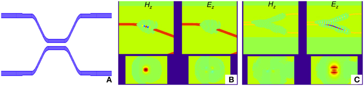
Figure 13. Simulation results from 3D sparse FDTD. (A) is the top view of the structure being simulated, which is a directional coupler. (B) Shows a screen shot from a simulation using a quasi-TE launch. The top two figures show the top views of the quasi-TE and quasi-TM signals, and the lower two figures show the corresponding cross-section views. (C) Shows a screen shot from a simulation using a quasi-TM launch.
7. Short Reach PICs
Short reach communications typically means less than 2 km, but can sometimes include up to 40 km. Short reach is usually for intra-data center, connecting racks, or client-side optics. There is an emerging need for very short reach communications in which boards are connected optically within a rack. Such optics are no longer considered “transceivers” and for the sake of focus are left out of this article.
Because of the fast growth and turn-over in data centers there is usually insufficient time for standards to develop. This allows for a wide diversity of solutions. These various solutions do not interoperate, but the users do not care so much, as long as prices are low.
Today, most of the short reach links are based on vertical-cavity surface-emitting lasers (VCSELs) over multimode fiber, i.e., do not involve PICs at all. VCSELs are very inexpensive and easy to couple to multimode fiber. It is nearly impossible for PICs to compete against VCSELs on price. However, the bandwidth-distance product for a VCSEL over multimode fiber is ~ 2 GHz-km. At 25 Gb/s, this limits distances to ~100 m. Also, multimode fiber (MMF) costs more than standard single-mode fiber (SSMF), because many more km of SSMF have been produced than MMF. Thus, when new data centers are built, it can be advantageous to outfit them with SSMF. Single-mode VCSELs are difficult to make today, so this is a good opportunity for PICs. However, VCSEL technology is constantly improving, providing a constant challenge to PICs in short-reach applications.
A successful PIC short-reach commercial solution today is based on parallel single-mode fibers (PSM). Figure 14 shows an 8-fiber PSM solution (4 fibers out and 4 fibers in) based on silicon photonics from Luxtera [40]. The chip contains a 1.4-μm laser in a small hermetic assembly on top of the PIC. This wavelength was chosen as optimum for the grating couplers that couple the laser light into the PIC. This laser is split four ways to four 10-Gb/s on-off-keying (OOK) distributed-driven Mach-Zehnder-interferometer modulators (MZMs). The CMOS drive electronics are monolithically integrated with the photonics. Distributed driven means that the modulator is broken into N sections in series, each with a separate driver timed appropriately. This saves power consumption over a traveling-wave modulator, because a traveling-wave modulator has a termination resistor into which power must be dumped.
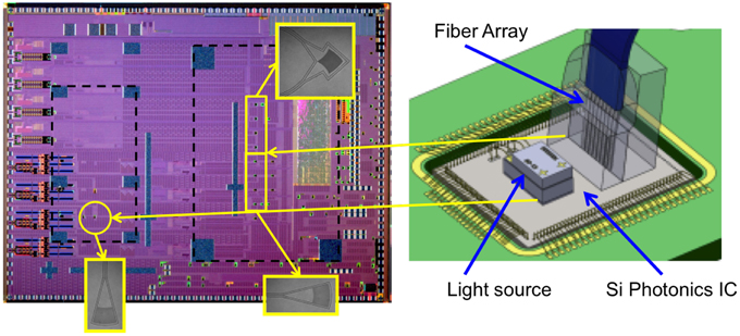
Figure 14. Silicon photonics 8-PSM transceiver. Courtesy of Luxtera.
Another successful PIC short-reach solution is based on wavelength-division multiplexing (WDM). Typically four wavelengths, each modulated with OOK at 25 Gb/s, are multiplexed in the transmitter and demultiplexed at the receiver. The advantage over PSM is requiring only two fibers instead of eight, and the disadvantage is requiring four lasers instead of one. WDM makes more sense as the cost of transceivers drops compared to the cost of fiber and installing it, especially ribbon fibers. Figure 15 shows an 8-channel CWDM receiver in silicon photonics [41]. It uses a silicon nitride spot-size converter and arrayed waveguide grating (AWG), which is polarization independent via variation of waveguide widths, silicon output multimode waveguides, and Ge photodetectors.
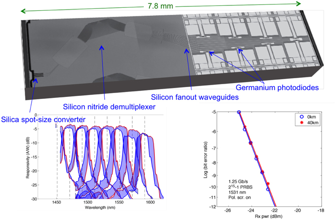
Figure 15. Silicon photonics 8-WDM receiver. The upper figure shows a photograph of the chip, the lower left figure shows the measured responsivities to the 8 detectors vs. wavelength, and the lower right figure shows the measured bit-error rate at 1.25 Gb/s for one of the channels using a polarization scrambler.
Yet another solution is to use multi-level modulation, called pulse amplitude modulation (PAM). Figure 16 shows PAM4 and PAM8 eye diagrams at 28 Gb/s generated by a silicon photonics MZM.
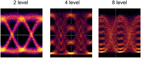
Figure 16. Measured PAM-2, -4, and -8 optical eye diagrams at 28 Gbaud using a silicon photonics modulator.
One can also use polarization-division multiplexing (PDM), also called dual-polarization (DP) transmission. In this case, different signals are in each polarization. Figure 17 shows a dual-polarization 80-Gb/s modulator in InP [42]. Such a design could be readily made in silicon photonics. In the fiber, the two signals will stay predominantly orthogonally polarized, but the polarization will vary unpredictably with time. At the receiver, if one does not use coherent detection, one needs to optically demultiplex the two polarizations. Figure 18 shows a device in silicon photonics that can optically demultiplex polarization [43, 44]. It does this by receiving two orthogonal polarizations from the fiber, these polarizations not necessarily that of the signals, and then interferes the two with a controllable phase and coupling ratio to demultiplex them. To do this in an endless fashion, i.e., without ever needing phase-shifter resets back to zero, one needs multiple interferometer stages.
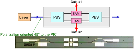
Figure 17. 80-Gb/s dual-polarization transmitter in InP. It consists of two electro-absorption InGaAsP modulators, a polarization splitter, and a polarization combiner. The incoming laser has its polarization oriented at 45°.
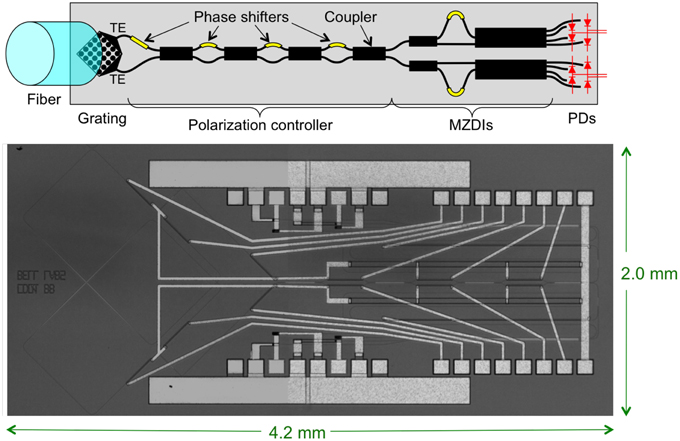
Figure 18. DP-DQPSK receiver in silicon photonics. Uses optical polarization tracking. The upper figure shows a schematic, and the lower figure a device photograph. The incoming signal is separated into two polarizations by a 2D grating coupler, a series of couplers and phase shifters demultiplex the two signals, which had been mixed during fiber transmission, and two Mach-Zehnder delay interferometers demodulate the signals.
In the far future one may find the data center interconnections so crowded that one must reduce the number of fiber strands and instead put multiple cores and/or modes in a single fiber. Figure 19 shows a PIC for receiving from a 7-core fiber, using polarization diversity [45]. It includes optical filters for WDM. Figure 20 shows a PIC for receiving from a multi-mode ring-core fiber [46]. A multi-mode ring core fiber is advantageous because the modes can be accessed without waveguide crossings and conveniently demultiplexed by a star coupler.
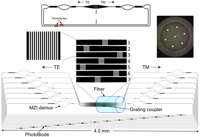
Figure 19. 7-core-fiber silicon photonics receiver. The upper right figure shows a photograph of the fiber cross section, showing the seven cores. The top shows the schematic for each channel in the silicon photonic circuit shown in the bottom figure. The incoming fiber is tilted at the proper angle to the 1D grating couplers such that TE polarization couples to the left and TM polarization couples to the right.
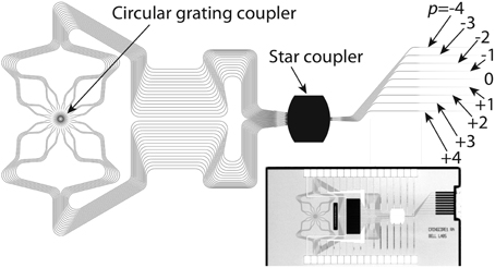
Figure 20. PIC for coupling to the multimodes of a ring-core fiber by using a circular grating coupler connected to a star coupler. The upper figure shows a schematic of the silicon photonic circuit photograph shown at the bottom. The circuit contains a circular grating coupler connected to an array of waveguides of equal length.
8. Metro and Long-reach PICs
Unlike short-reach links, which we saw have many choices of transmission type, metro and long-reach links demand intradyne coherent transmission. This is because long fiber routes are expensive to install/obtain, and thus the user wants to push as much information over each fiber as possible. Coherent receivers make it possible to receive WDM, PDM, and high-order constellations with high-performance, because the complete optical field is received and acted on by a DSP. In intradyne coherent communications, the transmitted signal comes from a dual-polarization vector modulator, and the received signal is interfered with a continuous-wave (CW) laser signal whose frequency is close to the carrier of the signal (within ~2–3 GHz), but does not need to be exact.
The first reported vector modulator was a GaAs PIC, shown in Figure 21 [47]. It consists of two MZMs in a larger interferometer. Figure 22 show some early vector modulators in silicon photonics. The modulator in Figure 22A contains two vector modulators, one for each polarization, along with the polarization splitting optics [48]. The single-polarization modulator in Figure 22B uses a thin-oxide layer in the p-n junction to obtain a low VπL product and is driven directly by CMOS inverters [49]. By using multiple segments in the modulator, one can create an optical digital-to-analog converter (DAC). The segment lengths are in a geometric sequence. Figure 23 shows a demonstration that achieved 16-QAM modulation at 13 Gbaud using a silicon photonic optical DAC [50].
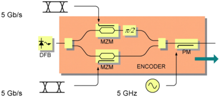
Figure 21. First reported vector modulator. It was in GaAs.
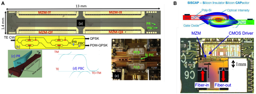
Figure 22. Early reported silicon photonic vector modulators.
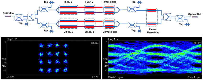
Figure 23. 2-bit optical DAC in silicon photonics.
The first reported coherent receivers were in InP, as shown in Figure 24A [51–55]. Figure 24B shows an early dual-polarization, dual-quadrature receiver in silicon photonics [56]. It uses a 2-D grating coupler as a fiber coupler, polarization splitter, and polarization rotator.
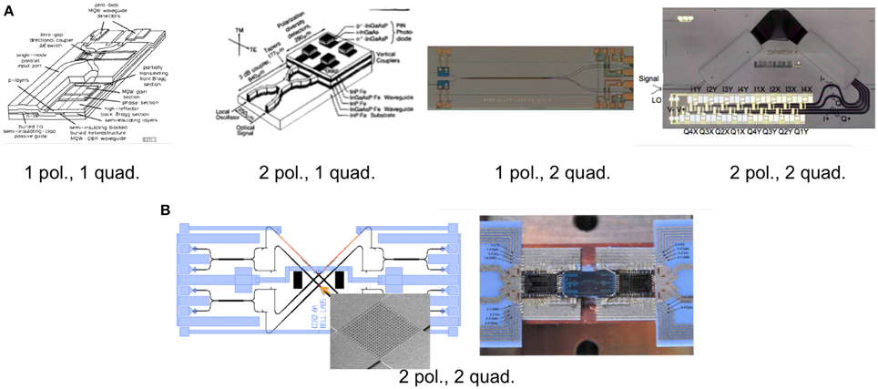
Figure 24. Early (A) InP and (B) silicon integrated coherent receivers.
Figure 25 shows a recent silicon photonic PIC that contains the full vector modulator and full coherent receiver on a single chip [4]. This is lower cost and smaller footprint than separate transmitter and receiver chips. There are three fibers connected to the module: laser input, which is split between transmitter and receiver; transmitter output; and receiver input. The fibers are connected in a 3-fiber array, reducing cost and assembly time. It is co-packaged in a hermetic gold box with four drivers and four transimpedance amplifiers. It does not require any temperature control, allowing the total power consumption to be less than 5 W, −5 to 80°C. A silicon photonics modulator does have some imperfections compared to Pockels-effect modulators, like GaAs and LiNbO3. It has residual amplitude modulation, diode nonlinearity, capacitance change with voltage, and bandwidth limitations. A simulation including these effects shows that the imperfection performance penalty is only 0.1 dB compared to an ideal modulator.
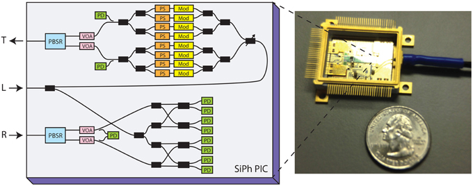
Figure 25. Single-chip silicon photonic coherent transceiver.
Each PIC was tested in a socket in an optical loop-back configuration using a 100-Gb/s DSP for real-time measurements, as shown in Figure 26A. Optical loop-back insures that any potential crosstalk between the transmitter and receiver would show up as degradation. Figure 26B shows a measured 30-Gbaud DP-QPSK eye diagram. There are five levels in such a signal. Figure 26C shows measured real-time-processed 120-Gb/s DP-QPSK constellations. Measured BER vs. OSNR curves at multiple wavelengths across the C-band are shown in Figure 26D shown for comparison is the performance of discrete optics. The performance of the silicon PIC is nearly the same as the discrete optics. Figure 26E shows the performance at various temperatures, showing that the silicon photonics can indeed work without temperature control. Figure 26F shows the performance up to 3000 km without significant penalty. This shows that the chirp of the silicon photonics modulator is low.
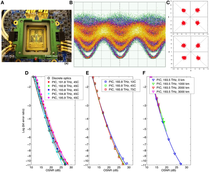
Figure 26. (A) Measurement setup, (B) measured 30-Gbaud eye diagram for DP-QPSK, (C) real-time-processed constellations at 120 Gb/s, and (D–F) bit-error rate vs. OSNR for various cases for the silicon photonics single-chip coherent transceiver in an optical loop back configuration.
Figure 27 shows this PIC in a 100-Gb/s CFP module. As one can see, the module is tightly packed and would be very difficult to make with discrete optics.
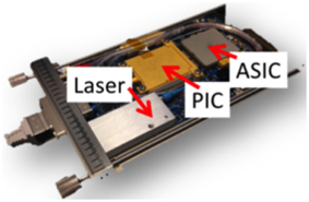
Figure 27. 100-Gb/s coherent CFP module using silicon photonics.
This single-chip coherent transceiver contains all the optics needed for a coherent transmitter except the tunable laser. As mentioned earlier, it is probably better to keep the laser separate anyways because this chip can be co-packaged with the DSP, which runs very hot.
9. Conclusion
The touted advantage of silicon photonics is the die are lower cost than any other solution. While this may be true, it is of limited help in short-reach applications, where the lack of an integrated laser puts silicon photonics at a significant disadvantage compared to the incumbents, such as VCSELs and DMLs. Instead, the less-touted advantages of silicon photonics: high yield, low modulator temperature sensitivity, high chip strength, and ability to do polarization handling; make it ideal for metro and long-haul applications. Spending its adolescence in metro and long-haul, silicon photonics will have time to develop mature laser integration methods, more routine foundry services, and sophisticated packaging solutions so it can later take on the short-reach incumbents. By that time, coherent transmission may be cost- and power-effective enough to work in very short links, bringing its advantages of high sensitivity, high spectral efficiency, high-order modulation, and wavelength selection.
Conflict of Interest Statement
The author declares that the research was conducted in the absence of any commercial or financial relationships that could be construed as a potential conflict of interest.
Acknowledgments
The author is indebted to Long Chen, Diedrik Vermeulen, Torben Nielsen, Scott Stulz, Saeid Azemati, Greg McBrien, Benny Mikkelsen, Christian Rasmussen, Mehrdad Givehchi, Seo Yeon Park, Jonas Geyer, Xiao-Ming Xu, and many others.
References
1. Winzer P. Advanced optical modulation formats. Proc IEEE (2006) 94:952–85. doi: 10.1109/jproc.2006.873438
2. Wellbrock G. Where do we go from here? In: OIDA Workshop on State of the Art Integrated Photonics. Washington, DC (2014).
4. Doerr CR, Chen L, Vermeulen D, Nielsen T, Azemati S, Stulz S, et al. Single-chip silicon photonics 100-Gb/s coherent transceiver. In: Optical Fiber Communication Conference: Postdeadline Papers. San Jose, CA (2014).
5. Taillaert D, Van Laere F, Ayre M, Bogaerts W, Van Thourhout D, Bienstman P, et al. Grating couplers for coupling between optical fibers and nanophotonic waveguides. Jpn J Appl Phys. (2006) 45:6071–7. doi: 10.1143/JJAP.45.6071
6. Mekis A, Gloeckner S, Masini G, Narasimha A, Pinguet T. A grating-coupler-enabled CMOS photonics plaform. J Sel Topics Quant Electron (2011) 17:597–608.
7. Chen L, Zhang L, Doerr CR, Dupuis N, Weimann NG, Kopf RF. Efficient membrane grating couplers on InP. IEEE Photon Tech Lett. (2010) 22:890–2. doi: 10.1109/LPT.2010.2047391
8. Shoji T, Tsuchizawa T, Watanabe T, Yamada K, Morita H. Low loss mode size converter from 0.3 um square Si wire waveguides to singlemode fibres. Electron Lett. (2002) 38:1669. doi: 10.1049/el:20021185
9. Chen L, Doerr CR, Chen YK, Liow TY. Low-loss and broadband cantilever couplers between standard cleaved fibers and high-index-contrast SiN or Si waveguides. IEEE Photon Tech Lett. (2010) 22:1744–6. doi: 10.1109/LPT.2010.2085040
10. Yamazaki H, Yamada T, Goh T, Kaneko A, Sano A. Integrated 100-Gb/s PDM-QPSK modulator using a hybrid assembly technique with silica-based PLCs and LiNbO3 phase modulators. In: European Conference and Exposition on Optical Communications Brussels: IEEE (2008). 1–4. doi: 10.1109/ECOC.2008.4729119
11. Fukuda H, Yamada K, Tsuchizawa T, Watanabe T, Shinojima H, Itabashi SI. Silicon photonic circuit with polarization diversity. Opt Express (2008) 16:4872–80. doi: 10.1364/OE.16.004872
12. Tang Y, Dai D, He S. Proposal for a grating waveguide serving as both a polarization splitter and an efficient coupler for silicon-on-insulator nanophotonic circuits. IEEE Photonics Technol Lett. (2009) 21:242–4. doi: 10.1109/LPT.2008.2010528
13. Taillert D, Chong H, Borel PI, Frandsen LH, Rue RMDL, Baets R. A compact two-dimensional grating coupler used as a polarization splitter. IEEE Photonics Technol Lett. (2003) 15:1249–51. doi: 10.1109/LPT.2003.816671
14. Soref R, Bennett B. Electrooptical effects in silicon. IEEE J Quantum Electron. (1987) 23:123–9. doi: 10.1109/JQE.1987.1073206
15. Zheng D, Smith B. Improved efficiency Si-photonic attenuator. Opt Express (2008) 16:16754–65. doi: 10.1364/OE.16.016754
16. Dong P, Chen L. Monolithically integrated VOA-MUX with power monitors based on submicron silicon photonics platform. Opt Fiber Commun Los Angeles, CA: IEEE (2012) 9–11. doi: 10.1364/ofc.2012.otu2i.5
17. Thomson DJ, Gardes FY, Fedeli JM, Zlatanovic S, Hu Y, Ping B, et al. 50-Gb/s silicon optical modulator. IEEE Photonics Technol Lett. (2012) 24:234–6. doi: 10.1109/LPT.2011.2177081
18. Liu A, Jones R, Liao L, Samara-Rubio D, Rubin D. A high-speed silicon optical modulator based on a metal âĂŞ oxide âĂŞ semiconductor capacitor. Nature (2004) 427:615–8. doi: 10.1038/nature02310
19. Liu J, Beals M, Pomerene A, Bernardis S, Sun R, Cheng J, et al. Waveguide-integrated, ultralow-energy GeSi electro-absorption modulators. Nat Photonics (2008) 2:433–7. doi: 10.1038/nphoton.2008.99
20. Liu M, Yin X, Ulin-Avila E, Geng B, Zentgraf T, Ju L, et al. A graphene-based broadband optical modulator. Nature (2011) 474:64–7. doi: 10.1038/nature10067
21. Ahn D, Hong Cy, Liu J, Giziewicz W, Beals M, Kimerling LC, et al. High performance, waveguide integrated Ge photodetectors. Opt Express (2007) 15:3916–21. doi: 10.1364/OE.15.003916
22. Assefa S, Xia F, Bedell S, Zhang Y. CMOS-integrated 40GHz germanium waveguide photodetector for on-chip optical interconnects. In: Optical Fiber Communication Conference (2009). p. 10–2. Available online at: http://www.opticsinfobase.org/abstract.cfm?id=177916
23. Kang Y, Liu H, Morse M, Paniccia M. Monolithic germanium / silicon avalanche photodiodes with 340 GHz gain-bandwidth product. Nat Photonics (2008) 3:59–63. doi: 10.1038/nphoton.2008.247
24. Michel J, Camacho-aguilera RE, Cai Y, Patel N, Bessette JT, Dutt BR, et al. An electrically pumped Ge-on-Si laser. In: Optical Fiber Communication Conference. Los Angeles, CA: IEEE (2012). p. 5–7.
25. Purnawirman, Sun J, Adam TN, Leake G, Coolbaugh D, Bradley JDB, et al. C-and L-band erbium-doped waveguide lasers with wafer-scale silicon nitride cavities. Opt Lett. (2013) 38:2–5. doi: 10.1364/OL.38.001760
26. Liu AY, Zhang C, Norman J, Snyder A, Lubyshev D, Fastenau JM, et al. High performance continuous wave 1.3 μ m quantum dot lasers on silicon. Appl Phys Lett. (2014) 104:3–7. doi: 10.1063/1.4863223
27. Fang A, Park H, Cohen O, Jones R, Paniccia M. Electrically pumped hybrid AlGaInAs-silicon evanescent laser. Opt Express (2006) 14:9203–10. doi: 10.1364/OE.14.009203
28. Roelkens G, Brouckaert J, Van Thourhout D, Baets R, NoÌĹtzel R, Smit M. Adhesive bonding of InPâĹŢInGaAsP dies to processed silicon-on-insulator wafers using DVS-bis-benzocyclobutene. J. Electrochem Soc. (2006) 153:G1015. doi: 10.1149/1.2352045
29. Marchena E, Creazzo T, Krasulick SB, Yu PKL, Van Orden D, Spann JY, et al. Integrated tunable CMOS laser. In: Optical Fiber Communication Conference (2013). Available online at: http://www.opticsinfobase.org/abstract.cfm?URI=oe-21-23-28048
30. Snyder B, Corbett B, O'Brien P. Hybrid integration of the wavelength-tunable laser with a silicon photonic integrated circuit. J Lightwave Technol. (2013) 31:3934–42. doi: 10.1109/JLT.2013.2276740
31. Jalas D, Petrov A, Eich M, Freude W, Fan S, Yu Z, et al. What is and what is not an optical isolator. Nat Photonics (2013) 7:579–82.
32. Levy M, Osgood RMJr, Hegde H, Cadieu FJ, Wolfe R, Fratello VJ. Integrated optical isolators with sputter-deposited thin-film magnets. IEEE Photonics Technol Lett. (1996) 8:903–5. doi: 10.1109/68.502265
33. Shoji Y, Mizumoto T, Yokoi H, Hseih IW, Osgood R. Magneto-optical isolator with silicon waveguides fabricated by direct bonding. Appl Phys Lett. (2008) 92:071117. doi: 10.1063/1.2884855
34. Bhandare S, Ibrahim SK, Sandel D, Zhang H, Wust F, Noe R. Novel nonmagnetic 30-dB traveling-wave single-sideband optical isolator integrated in III/V material. IEEE J Sel Top Quantum Electron. (2005) 11:417–21. doi: 10.1109/JSTQE.2005.845620
35. Doerr CR, Chen L, Vermeulen D. Silicon photonics broadband modulation-based isolator. Opt Express (2014) 22:4493. doi: 10.1364/OE.22.004493
36. Yee KS. Numerical solution of initial boundary value problems involving Maxwell's equations in isotropic media. Antennas Propagation IEEE Trans Livermore, CA: IEEE (1966). 302–7. doi: 10.1109/TAP.1966.1138693
37. Bienstman P, Baets R. Optical modelling of photonic crystals and VCSELs using eigenmode expansion and perfectly matched layers. Opt Quantum Electron. (2001) 33:327–41. doi: 10.1023/A:1010882531238
38. Doerr CR. Sparse finite difference time domain method. IEEE Photonics Technol Lett. (2013) 25:2259–62. doi: 10.1109/LPT.2013.2285181
39. Doerr CR. 3D sparse finite-difference time-domain simulation of silicon photonic integrated circuits. In: Optical Fiber Communication Conference. Los Angeles, CA (2015).
40. Narasimha A, Analui B, Liang Y, Member S, Sleboda TJ, Abdalla S, et al. A fully integrated 4 x 10-Gb / s DWDM optoelectronic transceiver implemented in a standard 1.3 um CMOS SOI technology. IEEE J Solid State Circ. (2007) 42:2736–44. doi: 10.1109/JSSC.2007.908713
41. Doerr CR, Chen L, Buhl LL, Chen YK. Eight-channel SiO2/Si3N4/Si/Ge CWDM receiver. IEEE Photonics Technol Lett. (2011) 23:1201–03. doi: 10.1109/LPT.2011.2158091
42. Doerr CR, Zhang L. Monolithic 80-Gb / s dual-polarization On-off-keying modulator in InP. J Lightwave Technol. (2008) 2:19–21.
43. Doerr CR, Chen L. Monolithic PDM-DQPSK receiver in silicon. In: Optical Communication (ECOC), 2010 36th European Conference and Exhibition on (IEEE) (2010). p. 1–3. Available online at: http://ieeexplore.ieee.org/xpls/abs_all.jsp?arnumber=5621418
44. Doerr CR, Fontaine NK, Buhl LL. PDM DQPSK silicon receiver with integrated monitor and minimum number of controls. IEEE Photonics Technol Lett. (2012) 24:697–9. doi: 10.1109/LPT.2012.2187048
45. Doerr CR, Taunay TF. Silicon photonics core-, wavelength-, and polarization-diversity receiver. IEEE Photonics Technol Lett. (2011) 23:597–9. doi: 10.1109/LPT.2011.2118748
46. Doerr CR, Fontaine N, Hirano M, Sasaki T, Buhl L, Winzer P. Silicon photonic integrated circuit for coupling to a ring-core multimode fiber for space-division multiplexing. In: European Conference and Exposition on Optical Communications (2011). Available online at: http://www.opticsinfobase.org/abstract.cfm?URI=ECOC-2011-Th.13.A.3
47. Griffin R, Johnstone R, Walker R, Wadsworth S, Carter A, Wale M. Integrated DQPSK transmitter for dispersion-tolerant and dispersion-managed DWDM transmission. OFC 2003 Optical Fiber Communications Conference (2003). p. 7–8. doi: 10.1109/OFC.2003.1248559
48. Dong P, Xie C, Chen L, Buhl LL, Chen YK. 112-Gb/s monolithic PDM-QPSK modulator in silicon. Opt Express (2012) 20:B624–9. doi: 10.1364/OE.20.00B624
49. Milivojevic B, Raabe C, Shastri A, Webster M, Metz P, Sunder S, et al. 112Gb / s DP-QPSK transmission over 2427km SSMF using small-size silicon photonic IQ modulator and low-power CMOS driver. In: Optical Fiber Communications Conference. San Jose, CA (2013). p. 5–7.
50. Shastri A, Webster M, Jeans G, Metz P, Sunder S, Chattin B, et al. Experimental demonstration of ultra-low-power single polarization 56 Gb / s QAM-16 generation without DAC using CMOS photonics. In: European Conference and Exposition on Optical Communications. Cannes (2014). p. 16–8.
51. Koch T, Koren U, Gnall R, Choa F, Hernandez-Gil F, Burrus C, et al. GaInAs/GaInAsP multiple-quantum-well integrated heterodyne receiver. Electron Lett. (1989) 25:1621. doi: 10.1049/el:19891086
52. Takeuchi H, Kasaya K, Kondo Y, Yasaka H, Oe K, Imamura Y. Monolithic integrated coherent receiver on InP substrate. IEEE Photonics Technol Lett. (1989) 1:398. doi: 10.1109/68.43392
53. Deri RJ, Pennings E, Scherer A, Gozdz A, Caneau C, Andreadakis N, et al. Ultracompact monolithic integration of balanced, polarization diversity photodetectors for coherent lightwave receivers. IEEE Photonics Technol Lett. (1992) 4:1238. doi: 10.1109/68.166954
54. Bach H, Matiss A, Leonhardt CC, Kunkel R, Schmidt D, Schell M, et al. Monolithic 90° hybrid with balanced PIN photodiodes for 100 Gbit / s PM-QPSK receiver applications. Optical Fiber Communication Conference (2009). p. 4–6.
55. Doerr CR, Zhang L, Winzer PJ. Monolithic InP multiwavelength coherent receiver using a chirped arrayed waveguide grating. J Lightwave Technol. (2011) 29:536–41. doi: 10.1109/JLT.2010.2097240
Keywords: integrated optics, silicon photonics, optical fiber, optical communications, coherent, gratings, waveguides
Citation: Doerr CR (2015) Silicon photonic integration in telecommunications. Front. Phys. 3:37. doi: 10.3389/fphy.2015.00037
Received: 11 February 2015; Paper pending published: 23 March 2015; Accepted: 13 May 2015;
Published: 05 August 2015.
Edited by:
Qiaoliang Bao, Soochow University, ChinaReviewed by:
Lukas Novotny, ETH Zurich, SwitzerlandSatoshi Iwamoto, The University of Tokyo, Japan
Xiangping Li, Swinburne University of Technology, Australia
Copyright © 2015 Doerr. This is an open-access article distributed under the terms of the Creative Commons Attribution License (CC BY). The use, distribution or reproduction in other forums is permitted, provided the original author(s) or licensor are credited and that the original publication in this journal is cited, in accordance with accepted academic practice. No use, distribution or reproduction is permitted which does not comply with these terms.
*Correspondence: Christopher R. Doerr, Acacia Communications, 1301 Route 36, Hazlet, NJ 07730 USA, chris.doerr@acacia-inc.com