Integration of functional complex oxide nanomaterials on silicon
 José M. Vila-Fungueiriño1
  Romain Bachelet2
  Guillaume Saint-Girons2
  Michel Gendry2
  Marti Gich3
  Jaume Gazquez3
  Etienne Ferain4
  Francisco Rivadulla1
  Juan Rodriguez-Carvajal5
  Narcis Mestres3
  Adrián Carretero-Genevrier2*
- 1Centro de Investigación en Química Biológica y Materiales Moleculares, Universidad de Santiago de Compostela, Santiago de Compostela, Spain
- 2Institut des Nanotechnologies de Lyon, Centre National de la Recherche Scientifique - École Centrale de Lyon, Lyon, France
- 3Consejo Superior de Investigaciones Científicas, Institut de Ciéncia de Materials de Barcelona, Barcelona, Spain
- 4Bio and Soft Matter, Institute of Condensed Matter and Nanosciences, Université catholique de Louvain, Louvain-la-Neuve, Belgium
- 5Diffraction Group, Institut Laue-Langevin, Grenoble, France
The combination of standard wafer-scale semiconductor processing with the properties of functional oxides opens up to innovative and more efficient devices with high value applications which can be produced at large scale. This review uncovers the main strategies that are successfully used to monolithically integrate functional complex oxide thin films and nanostructures on silicon: the chemical solution deposition approach (CSD) and the advanced physical vapor deposition techniques such as oxide molecular beam epitaxy (MBE). Special emphasis will be placed on complex oxide nanostructures epitaxially grown on silicon using the combination of CSD and MBE. Several examples will be presented, with a particular stress on the control of interfaces and crystallization mechanisms on epitaxial perovskite oxide thin films, nanostructured quartz thin films, and octahedral molecular sieve nanowires. This review enlightens on the potential of complex oxide nanostructures and the combination of both chemical and physical elaboration techniques for novel oxide-based integrated devices.
Introduction
Complex functional oxides display a wide range of properties: from colossal magnetoresistance and high-temperature superconductivity to ferroelectricity and multiferroicity. Consequently, oxides might provide a way to tackle large number of technological challenges including devices with lower energy consumption and transition to renewable sources of energy. In this context, silicon is to-date the most fundamental technological material in the electronics industry. Therefore, integrating high quality epitaxial oxide films and nanostructures on silicon is a milestone toward the fabrication of a number of devices based on the functionalities of oxides combined with the traditional Si-based complementary metal-oxide-semiconductor (CMOS) technology. The growth of structurally different materials on the same wafer represents a bottleneck in the development of new devices based on the coupling of the physical properties of these materials at the heterostructure level. Therefore, a successful integration of functional oxides on silicon offers an unlimited potential for new applications in electronics, optics and, optoelectronics. Consequently, large efforts are currently focused on matching dissimilar oxides (structurally, thermally, and in general chemically reactive) and silicon in hybrid structures.
In the past decade, complex oxides have been investigated as potential candidates to replace SiO2 in MOSFETs with the objective of bypassing the fundamental physical limitations and further enhancing the performance of this gate oxide. Thus, a large body of research is committed to new materials with higher dielectric constant for gate oxides (“high-k” oxides) [1, 2]. The research on the integration of functional oxides on silicon is mainly motivated by the use of oxides in electronics, from oxide electronics [3] and memories to sensing applications [4]. The field of integrated optics started to be investigated as a result of the unique electro-optical properties of transition metal oxides which could bring unprecedented and novel capabilities to the silicon platform. The direct integration on silicon by molecular beam epitaxy (MBE) of a ferroelectric BaTiO3 film exhibiting a strong linear electro-optic (EO) effect with a high effective Pockels coefficient has supposed a main breakthrough in the field [5, 6]. This strong EO response makes the film an optimal candidate as a base material for novel applications in the field of silicon photonics including modulators, tuning elements, and bistable switches.
In this review we describe the main strategies that have been successfully used to monolithically integrate functional complex oxide nanostructures on silicon via CSD methods and advanced physical vapor deposition techniques such as MBE. This review will also focus on recent advances combining CSD and nanoporous polymer templates with the epitaxial growth for the controlled design and growth of textured crystalline solids. This novel approach offers an attractive methodology to further integrate functional oxide nanostructures on silicon substrates. The review will mainly cover single-crystalline oxide films and nanostructures. Crystalline oxides present two main advantages: (i) the properties of a crystalline film or nanostructure are in general superior to those of the same material under an amorphous/polycrystalline form and (ii) their interfaces with silicon are better defined and therefore can be more effectively characterized and modeled.
Integration of Functional Oxides by Physical Methods
Functional oxide thin films and nanostructures can be produced through physical or chemical methods. The main physical deposition techniques that are typically used to grow epitaxial films and nanostructures of complex oxides are: (i) pulsed laser deposition (PLD), (ii) sputtering deposition, and (iii) molecular beam epitaxy (MBE) [7]. These three techniques fall within the broad category commonly known as physical vapor deposition (PVD), where chemical reactions are excluded or poorly involved in the growth mechanism.
PLD is a PVD technique dedicated to the fabrication of thin films. This technique consists in the deposition of a material on a substrate inside a vacuum chamber by focusing a high power pulsed laser beam that strikes a target composed of the elements that are to be deposited. The transfer of the material from the target to the substrate enables the direct deposition of complex multielement oxides. As a result, PLD method is an excellent lab-scale research tool for high rate deposition of epitaxial oxide films, multi-layer and superlattices systems. In this context, the growth of complex oxides through the sequential deposition from binary targets by PLD is currently being investigated in order to reach a precise atomic layer control over the interfaces [8].
Nevertheless, the up-scaling of complex oxides by using PLD is a major challenge that requires a nanoscale precision over large areas and high deposition rates. Recently, large-area deposition of functional oxide thin films such as piezoelectric Pb(Zr,Ti)O3 (PZT) for micro-electronical-mechanical systems (MEMS) and nanoelectromechanical systems (NEMS) applications, ionic conducting Yttria-stabilized zirconia (YSZ) for fuel cells or transparent electrical conducting layers on sensitive substrates, like flexible displays and OLED, with PLD on wafers up to 200 mm diameter were obtained [9].
Magnetron sputtering is also a PVD technique widely used for the growth of thin films, including metal oxides. It is based on the ejection of atoms from a target surface by the transfer of kinetic energy of incoming energetic ions, usually Ar+ generated in a plasma [10]. The kinetic energy of the impinging ions ranges from 50–1000 eV with an energy distribution peaking at around 10–40 eV. This growth technique grants a stoichiometric transfer from the target material to the substrate allowing the growth of multi-element compounds in large areas (>4 in. wafer). However, PLD allows obtaining more easily a precise stoichiometry of complex oxides films which can be controlled with the deposition pressure [11].
MBE is also another vacuum deposition method in which well-defined thermal beams of atoms or molecules react at a crystalline surface to finally produce an epitaxial film [12]. Each molecular beam is created by separated effusion cells, which operate at different temperatures to provide the desired element flux [13]. In this context, MBE offers excellent stoichiometric compositional control because effusion cells can evaporate homogeneously and separately different elements. However, the growth rate of complex oxide films via MBE is very slow and expensive. As a consequence, MBE and PLD have important differences regarding the instantaneous deposition rate during thin films growth. As an example, the typical growth rate for MBE is 1 monolayer (ML) per second, while in PLD the instantaneous growth rates can reach 1 ML/microsecond, i.e., six orders of magnitude faster. Indeed, the average growth speed for PLD is limited only by the repetition rate of the laser. Thus, PLD technique can perform a variety of fundamental kinetic studies that are difficult to be achieved by using MBE technique.
Figure 1 shows a schematic representation of the key elements of a MBE dedicated to epitaxial oxide growth. Interestingly, MBE is equipped with a reflection high energy electron diffraction (RHEED) system, which is an in-situ analytical tool that is used during the epitaxial growth. Thus, RHEED is commonly used to calibrate beam fluxes or alloy compositions and thicknesses in multilayer systems. Notice that MBE is almost the only technique allowing epitaxy of different oxides on different semiconductor platforms due to the careful surface passivation strategies, slow atomic layer-by-layer depositions, and the control of very low oxygen partial pressures. Different oxide systems have been prepared by MBE on semiconductor substrates, including perovskites on Si(001), Ge(001), or GaAs(001) [14–16], bixbyites on Si(111) [17], or spinels on Si(111) [18].
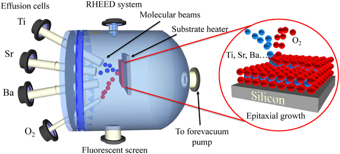
Figure 1. Schematic of an oxide-MBE (O-MBE) setup that shows the epitaxial integration of perovskite based-oxides on silicon through a metallic evaporation under oxygen.
PLD and sputtering are much more mature than MBE for the growth of oxides, but MBE technique offers some advantages such as broader homogeneity over large surfaces and flexibility of doping compared to PLD. More importantly, MBE provides advanced control of the interfaces and growth processes, which allows the development of interface engineering strategies to grow functional oxides on Si and other semiconductor platforms [7, 19, 20].
Epitaxial growth of complex oxides on silicon is far from straightforward as a result of material dissimilarities. Most of the strains are linked to the fact that a crystalline oxide on a semiconductor induces a transition from a network of strongly covalent bonds in silicon to a mode of primarily ionic bonding in the oxide over a length-scale of less than a nanometer [21]. As a result, in addition to the overall film stoichiometry, it is crucial to monitor the thermodynamics of each layer during the growth process in order to control the heteroepitaxial transition. The formation of amorphous SiO2 or silicates layers during the first stages of the growth process might hinder epitaxy. Therefore, the partial pressure of the oxygen and the silicon temperature need to be controlled throughout the process.
A breakthrough in the MBE field was made by McKee et al. [19], where the authors employed surface passivation with a half-monolayer Sr on Si(001) to grow an epitaxial SrTiO3 (STO) layer on Si(001). The major advance of introducing such layer was to prevent the formation of amorphous silicon oxide on the Si surface in order to boost the growth of STO. Since then, STO/Si(001) has been used as a large-scale pseudo-substrate for the integration and development of functional perovskite oxides on Si [5, 22–26]. Following the same philosophy, Yttria-stabilized zirconia (YSZ) grown by PLD has also been used as an effective buffer layer to develop the technology of oxide films on Si(001) [27]. This resulted in the integration of functional ferromagnetic spinel oxides [28] or ferroelectric perovskite oxides [29].
Integration of Functional Oxides by Chemical Methods
Chemical vapor deposition (CVD) is a process widely used in industry for the growth of thin films as a result of its good stability and reproducibility. Thus, it is used in a broad array of applications. CVD is based on the deposition of a thin solid film onto a substrate through chemical reaction of gaseous species [30]. The main difference between CVD and PVD methods relies on the reactive process. In this case, the final product is what dictates the different energy sources, the precursor gases, and the substrates to be used. The thermal decomposition of the precursor gives rise to a thin film deposit. Ideally, along the process the ligands that are associated with the precursor are cleanly eliminated to the gas phase in the form of reaction products.
Atomic layer deposition (ALD) is based in the sequential transfer of precursors or reagents that either adsorb to saturation coverage or undergo selective ligand reactions. On either case, the process is self-limiting thus, leading to a layer-by-layer growth of an atomic film [31, 32]. As a result, this growth technique can provide atomic layer control and the deposition of ultrathin conformal films onto very high aspect ratio structures. ALD is thus a CVD technique based on sequential, self-terminating and, gas—solid reactions.
The main advantages of chemical solution method as an alternative approach to grow functional oxide thin films and nanostructures are their low cost and easy setup, the good control over stoichiometry, the use of dopants, and the coating of large and uniform areas. In a typical chemical solution deposition (CSD) method the growth process is based on three steps: [1] The preparation of a homogeneous and stable precursor solution; [2] the deposition of a thin film onto a substrate either through spin coating, dip coating, or spray coating; [3] a low-temperature thermal treatment to form an amorphous film by removing the solvent, and a high-temperature thermal treatment which allows the densification and crystallization of the films (see Figure 2). Therefore, chemical solution based methods encompass a broad range of techniques including sol-gel techniques, chelation, metal-organic decomposition, polymer-assisted deposition (PAD), and hydrothermal methods (see for in-depth details on CSD methodology [33–37]).
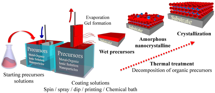
Figure 2. Scheme of the formation of epitaxial thin films of perovskite-based oxides via solution processing routes (dip-coating).
Low-temperature processing profile of functional oxides by CSD offers a variety of strategies to overcome the problems associated to final heating temperatures during the integration into microelectronic elements and related devices. The crystallization temperatures of thin films with different chemical compositions are decreased by conveniently modifying the precursor solution and designing the heating profile to ensure a high level of chemical homogeneity already in the liquid state and throughout the processing. In this context, UV irradiation assisted deposition of ferroelectric thin films at temperatures as low as 450°C is a suitable strategy for the integration into the CMOS technology [38, 39]. Light-sensitive materials containing UV absorbing species (like β-diketonates) were formed by tailoring the chemistry of the sol-gel precursors. The subsequent UV irradiation produces the pyrolysis and oxidation of the organic components of the sol-gel film, which makes possible the formation of the M-O-M bonds of the ferroelectric perovskite at low temperatures.
Another strategy is based on the incorporation of seeds into the photoactive sol. This enlarges the number of nucleation sites in the emerging film, leading to a reduction of the crystallization temperature [40]. In this direction, lead zirconate titanate (PZT) attains a lower limit of crystallization temperature at 300°C [41], therefore allowing the use of these multifunctional oxide layers as advanced devices supported on flexible polymeric substrates.
In addition, bismuth ferrite BiFeO3 (BFO) thin films have been successfully prepared onto silicon and Pt-coated silicon substrates at low temperatures (400°C) using a synthesis strategy based on the use of purely water-based systems and nonhazardous reagents [42, 43].
Likewise, the low deposition temperatures normally used in ALD offer promising chemical routes for the integration of crystalline oxides on Silicon. As an example, single crystalline anatase TiO2 thin films have been epitaxially grown on silicon by ALD as a potential platform for memories based on resistive switching [44]. Moreover, epitaxial STO and Al-doped STO films up to 15-nm thick with a high-degree of crystallinity were grown on the (001)-Ge substrates via ALD for high mobility Ge-based transistors [45].
Toward the Combination of Growth Techniques
The growth of crystalline oxides on Si by combining physical and chemical methods is also a matter of current research that in the recent years has enhanced the integration of novel functional oxides with multiple applications. In this context, the combination of MBE and ALD has been intensively studied. As an example, a four-unit-cell STO buffer layer grown by MBE was engineered to provide a stable template for the posterior growth of crystalline oxides by ALD on (001)-Si. This methodology resulted in the successful growth of epitaxial anatase TiO2, SrTiO3, LaAlO3 and BaTiO3 thin films [46–49].
A new approach combining MBE and PAD has been recently introduced by the authors for the growth of integrated functional oxide thin films on silicon substrates. PAD is a wet chemical method introduced by Jia et al. [34] that uses aqueous solutions of polymers and metallic salts. The polymer plays a significant role in the process by controlling the desired viscosity of the precursor without gelling and additionally, binding the metal ions to prevent premature precipitation and the further formation of metal-oxide oligomers. This process leads to a homogeneous distribution of the metal precursors in the solution. Polyethyleneimine (PEI) and its derivatives are the most frequently used polymers in PAD and metal nitrates, metal chlorides, metal acetates, or metal hydroxides are among the source of metals widely used. As an aqueous solution system, PAD is less dependent on expensive or sensitive metalorganic precursors, thereby lowering the environmental impact, if compared to other chemical solution methods. As an example, PAD was shown to produce films of high quality and abrupt interfaces were obtained in epitaxial multilayers [34, 50].
In this direction, the authors present a novel example in Figure 3 that shows a HAADF-STEM image of a LaCoO3 (LCO) cobaltite thin film (15 nm) deposited by PAD on top of a STO buffer (10 nm) grown by MBE on a (001)-Si substrate with sharp interfaces (see Figure 3). The strain state of the cobaltite film and its influence on the physical properties are currently under investigation. We found that the structural quality and the sharpness of the interfaces are similar in the layers grown by MBE and by PAD.
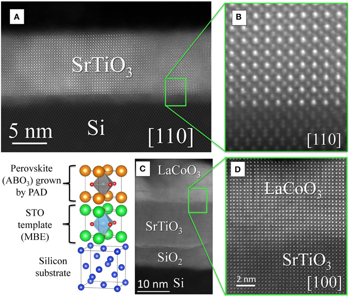
Figure 3. (A) Cross-sectional HAADF-STEM image of a STO thin film epitaxially grown on silicon substrate by MBE (450°C). (B) Enlarged view of the interface showing the epitaxial relationship between STO film and silicon substrate according to [100] STO//[110] silicon. (C) Cross-sectional HAADF-STEM image of a LCO cobaltite thin film deposited by PAD (800°C during 2 h) on top of a STO buffer layer grown by MBE on a (001)-Si substrate. (D) Magnified view of the interface exhibiting the epitaxial similarity between STO buffer layer and LCO film. All images were acquired with a Nion UltraSTEM 100 dedicated aberration-corrected STEM, operated at 100 kV, which features an atomic-size probe ~1.0Å HAADF-STEM imaging resolution.
From Thin Films to Nanostructured Surfaces
Nanostructured surfaces are interesting in many fields as a result of their many applications including electronic devices, storage media, and as substrates for the production of more complex structures. Notice that periodically organized mesoporous architectures exhibit unexpected electrochemical, catalytic and photo-catalytic properties. As a result, mesoporous networks work as a connected solid network that allows fast transport of electrons, oxygen ions or protons. The construction of porous and hierarchically structured materials is accomplished by bridging together sol-gel chemistry, multiple templating, and advanced processing, namely Integrative Chemistry Strategy. The main chemical routes and strategies in this direction have been thoroughly described in several review articles [51–53].
Oxide nanostructures of high quality and low aspect-ratio (ratio of out-of-plane to in-plane dimensions) can be obtained by self-assembly patterning methods based on CSD. In self-assembly of oxide nanostructures, solution precursors are spin-coated on a substrate pursued by a high temperature annealing. Concerning ultrathin layers of a precursor prepared at high temperatures (commonly 600–900°C), the crystallized oxide “breaks down” into minor islands, creating small crystallites in order to minimize the entire surface and interface energies [54, 55]. The shape of the nanostructures and their distribution are largely determined by the misfit strain between the substrate and the functional oxide itself. The shape of the nanoislands can be stabilized by the convenient selection of the substrate's crystallographic orientation. The main improvement of these self-assembly techniques are the low costs, their simple processing, and the absence of patterning conditions. However, to-date high quality crystalline oxides have been established only for epitaxially grown structures and the nanostructures size, shape and precise position cannot be efficiently controlled.
The CSD process is so far an adaptable method that can be assembled with the use of molds or templates with high aspect ratio nanopores infiltrated with the convenient chemical precursors. This results in the fabrication of low or high aspect ratio oxide nanostructures [56]. As an example, porous Si and alumina templates as well as polymers patterned through e-beam, ion beam or photo-lithography, and block co-polymers in self-assembly have been described as successful templates [57–60]. Following this approach, nanorings of perovskite PZT with internal diameters down to ~5 nm and ring thicknesses of ~5–10 nm have been well fabricated by chemical solution deposition on the pore walls of nanoporous alumina membranes made on silicon substrates [61].
Nevertheless, submicron size nanostructures in a well-defined arrangement are required for many interesting applications such as ferroelectric or ferromagnetic memory applications. High-density ferroelectric nanostructure arrays have been fabricated using a heated AFM tip on sol-gel precursor films deposited onto platinized or plain Si substrates [62].
In addition, fully functional arrays of ferroelectric and ferromagnetic nanostructures can be prepared by electron-beam direct writing (EBDW) [63, 64]. In EBDW, the chemical reactions are narrowly activated in a metallorganic thin film after irradiation with an EB under adequate energy and dose and the required pattern is impressed by scanning the EB over the sample. The pattern is completed by dissolving the unexplored area in a precise solvent and further converted into metal oxide by thermal annealing. The major advantage of this processing method is its “direct writing,” which allows a user-specified shape, size, and positioning of the nanostructure on the substrate [63].
Growth of Functional Oxide Nanostructures on Si Substrates by Epitaxial Quartz Templating
In the past decades, most of the works on the growth of crystalline oxide thin films on silicon have been based on a layer-by-layer approach to heteroepitaxy. The main techniques used to this purpose have been MBE or PLD after adjusting the growth conditions during the deposition to avoid silicon surface oxidation. However, such techniques cannot be used to grow integrated functional oxide nanostructures and thick films. In the last years, CSD showed up as a versatile bottom-up approach to generate nanostructured surfaces and thicker films. In this regard, the authors recently established that the combination of soft chemistry and epitaxial growth expands opportunities for the controlled growth of functional oxide nanostructures on silicon. As an example, Carretero-Genevrier et al. used silicon substrate to develop structured epitaxial piezoelectric quartz thin films [65]. In this work authors employed industrial dip-coating method to produce quartz thin films on (100)-silicon substrates of controllable thicknesses from sol-gel precursors. The dip-coating process was executed in four stages: (i) immersion of the silicon substrate inside the sol-gel solution of the coating material at a constant speed, (ii) deposition of the thin layer on the silicon substrate while it is pulled up at a constant speed for a good control of the thickness of the film, (iii) drainage of the excess liquid from the surface of the substrate; and (iv) evaporation of the solvent and gelification of sol-gel precursors forming the thin film. In this case, the sol-gel solution contained partially hydrolyzed and condensed tetraethoxysilane (TEOS) as a quartz precursor and specific proportions of Sr2+, Ba2+, or Ca2+, which functioned as silica network modifiers [66]. Indeed, a homogeneous distribution of these alkaline earth metals within the amorphous silica film during dip coating process offered the potential to thermally induce the epitaxial growth of α-quartz films on silicon by a catalytic devitrification of the silica native layer at the silicon interface (see Figure 4). Importantly, the authors observed that the low mismatch between the (100)-quartz plane and the crystalline (100)-silicon substrate induced the nucleation of α-quartz crystals at the silicon-silica interface during thermal treatment above 900°C (5 h in air at ambient pressure). In that case, other polymorphs of silica did not show an equal mismatch with the silicon substrate thus, preventing the stabilization of other crystalline silica phases [65]. This particular growth mechanism was coupled along with the CSD methodology to control the nanostructuration of piezoelectric quartz thin films. As an example, Figure 4 shows the crystallization of macroporous silica films at 1000°C in the presence of Sr2+, Ba2+, or Ca2+ as devitrifying agents. The piezoelectric functionality of these nanostructured films was completely preserved and no important differences between the piezoelectric force microscopy (PFM) response inside and outside regions of the pore were found [67].
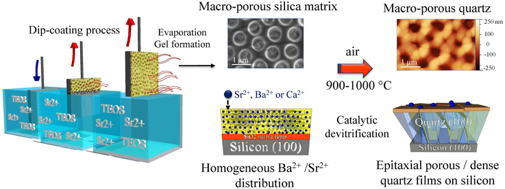
Figure 4. Crystallization mechanism of nanostructured epitaxial α-quartz thin films on silicon substrate. Note that this growth mechanism is prepared by a dip-coating process. During the gelification and drying of films, strontium, barium or calcium ions were uniformly distributed within the amorphous silica matrix. After crystallization thin films maintain the initial porous structure achieved at room temperature. The nucleation of crystals quartz at the silicon-silica interface takes place over 900°C just after a devitrification mechanism that result in a monooriented polycrystalline quartz film.
Compared to standard method of production of quartz films, top down technology based on cutting and polishing of large hydrothermally grown crystals, this bottom-up approach that produces nanostructured quartz films allows obtaining much thinner films with thicknesses between 150 and 750 nm. The thicknesses of the quartz films obtained by standard method cannot be below 10 μm and for most applications these need to be bonded on Si substrates. As a consequence, quartz films obtained by this novel approach could find applications in the future in the field of electromechanical devices because thanks to its thicknesses below 500 nm these are expected to present higher resonance frequencies.
Moreover, the authors have recently evidenced that epitaxial quartz films on silicon are intrinsically chiral. In this work, a comparative evaluation of the surface energies of the two possible trapezoidal habits in the P3121 and P3221 quartz space groups was performed. Authors founded significant differences in the number of dangling bonds per unit area for the (−131) surfaces, providing evidences of an enantiomer selection mechanism of the two single possible trapezoidal habits. This work importantly opens new perspectives in the field of enantioselective surface chemistry and in the mechanisms governing crystallization of chiral pure systems [68].
Analogously, it is possible to take advantage of the catalytic devitrification process of the silica native layer at the silicon interface for the epitaxial stabilization of complex oxide nanowires on silicon as shown by Carretero-Genevrier et al. In that case, the authors used supported track etched polymeric templates as a nanoreactor for the confined growth and further stabilization of epitaxial oxide nanowires on silicon [69]. The nucleation and crystalline growth of these 1D nanostructures was detected when Sr2+, Ba2+, or Ca2+ cations were present in the precursor solution. Importantly, the homogeneous dissemination of these catalyst cations was needed for the crystallization of interfacial α-quartz layer as result of the confinement of the precursor solution within the nanoporous template.
The confined nucleation and growth mechanism is extensible to different nanowire compositions, as long as the initial nanowire precursor solution contains Ba2+, Ca2+, or Sr2+ as devitrifying agents. Using chemical solution deposition the authors proved that it is possible to synthesize different single crystalline epitaxial octahedral molecular sieve (OMS) nanowire films including Ba1 + δMn8O16 hollandite, Sr1 + δ Mn8O16 strontiomelane, (BaSr)1 + δ Mn8O16 and a novel crystallographic phase named LaSr-2 × 4 OMS on top of (100)-silicon substrates [70] (see Figure 5). Importantly, the LaSr-2 × 4 OMS nanowires have shown augmented ferromagnetic properties with a Curie temperature above 500 K as a result of its particular crystallographic structure [71].
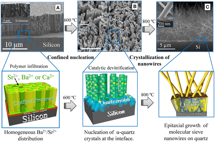
Figure 5. FE-SEM images and graphics (below) representing the intermediary steps during the OMS nanowires epitaxial growth on Si. (A) FE-SEM Cross-sectional image of the porous polymer template after infiltration of nanopores with the precursor solution. At this stage Ba2+, Sr2+, or Ca2+ cations are homogenously distributed. (B) FE-SEM image of the sample quenched at 600°C. Precursor nanocolumns that maintain the dimensions of the initial template nanopores are developed. At this step, the porous template has been disintegrated and the devitrification of SiO2 native layer and nucleation of α-quartz occurs at the interface. (C) FE-Cross-section SEM image of the nanowires grown on top of the α-quartz/Si substrate at 800°C.
The growth process of LaSr-2 × 4 OMS nanowires on Si substrates has been well established in recent works [70–72]. The confinement imposed by a polymer template during thermal treatment results in the formation of ε-MnO2 nanoparticles in the early stages of the growth process at low temperatures (up to 500°C). These nanoparticles will act as seeds for the growth of manganate nanowires under high temperature conditions (i.e., 800°C). In addition, the close contact of the silica native layer with the alkaline-earth metal cations present in the precursor solution during the thermal treatment assists the devitrification of the silica native layer. This melting process allows the crystallization of an intermediate α-quartz film and to further stabilize LaSr-2 × 4 OMS manganese oxide nanowires that crystallize in new monoclinic crystallographic structure.
The α-quartz films render a better lattice matching to the complex oxide nanostructures therefore, promoting the epitaxial growth of the LaSr-2 × 4 nanowires. However, due to the low annealing temperature (800°C), the α-quartz layer grown on (100)-Si substrates is polycrystalline, which results in the growth of nanowires along with different orientations with respect to the substrate plane.
The structural, electronic and magnetic structure of LaSr-2 × 4 manganese oxide molecular sieve nanowires were investigated by aberration corrected scanning transmission electron microscopy (STEM), in combination with electron energy loss spectroscopy (EELS). This combination has shown to be a powerful technique for structural, chemical and magnetic analysis down to the atomic scale [73].
The proposed unit cell of LaSr-2 × 4 nanowires based on X-ray diffraction and STEM analysis, is monoclinic with lattice parameters a = 13.8 Å, b = 5.7 Å, c = 21.8 Å, and β= 101°, where the long axis of the nanowires is along the b crystallographic direction. High resolution TEM images reveal that the orientation relationship can be described as (010) LaSr-2 × 4//010) α-quartz and an in-plane epitaxial relationship given by [20-2] LaSr-2 × 4// [−101] α-quartz (see Figure 6). STEM-EELS studies confirmed the uniform composition of the nanowires. It is worth mentioning that neither appreciable inter-diffusion of Si into the nanowires nor any trace of Sr on the quartz layer was detected by EELS studies (see Figure 6).
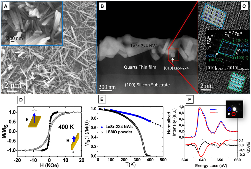
Figure 6. (A) Low magnification and high magnification (in inset image) field emission gun scanning electron microscope (FEG-SEM) images of epitaxial LaSr-2 × 4 nanowires on α-quartz/Si substrate. (B) Low magnification HAADF image of the quartz film and LaSr-2 × 4 nanowires interface. (C) High-resolution transmission electron microscopy (HRTEM) image exhibiting the epitaxial relationship between LaSr-2 × 4 nanowires and the α-quartz conforming to [20-2] LaSr-2 × 4//[−101]. (D) Hysteresis loops of the LaSr-2 × 4 nanowires registered at 400 K. Notice that both filled symbols and open symbols in the plot mean fields experimented parallel, and orthogonal to the substrate surface respectively. (E) Temperature tendency during field-cooled (FC) measurement at H = 1.5 T orthogonal to the substrate of LaSr-2 × 4 nanowires and powder blank samples. (F) Dichroism measurement and Mn L2, 3 edges, along the two polarized configurations (+) and (−).
The magnetism of LaSr-2 × 4 nanowires has been studied using electron magnetic circular dichroism (EMCD) (see Figure 6F), which can be measured from TEM after analysis of L2, 3 EELS absorption edges of transition metals [74]. EMCD measurements performed on a single LaSr-2 × 4 nanowire at room temperature showed that there is a significant orbital component to the magnetic moment and that this is aligned antiparallel to the spin moment [73]. This finding suggests that Mn shells are less than half-filled and that the origin of ferromagnetism may reside in a double-exchange-like mechanism. Indeed, the spatially resolved EELS measurements confirmed the presence of mixed-valence Mn cations at different sites, as a result of the ordered arrangement of the La3+ and Sr2+ cations within the structure. However, the electronic structure of these monoclinic LaSr-2 × 4 nanowires was different from its perovskite-like counterparts and the fine structure of the O-K edge presented significant changes compared to manganites [75, 76]. The different disposition and arrangement of La and Sr cations in the new structure of the nanowires might well affect the Mn-O bonds of MnO6 octahedra. Further theoretical work is thus needed to interpret the features of the electronic structure of LaSr-2 × 4 monoclinic nanowires.
In addition to the solution template-based growth methodology, the authors are investigating a novel strategy for the epitaxial integration of oxides nanowires on different substrates. This new procedure consists in the use of the MBE technology to allow the metallic evaporation under atomic oxygen inside the pores of supported track etched polymer templates (see Figure 7). As an example, the authors have successfully prepared BaTi5O11 nanowires on LaAlO3 (LAO) substrate using this approach. The epitaxial relationship of BaTi5O11 and its influence on the physical properties are currently under investigation. This finding proves once more that the confined growth of metastable phases within nanopores combined with an epitaxial growth offers interesting opportunities for the further integration of functional oxide nanowires on silicon substrates.
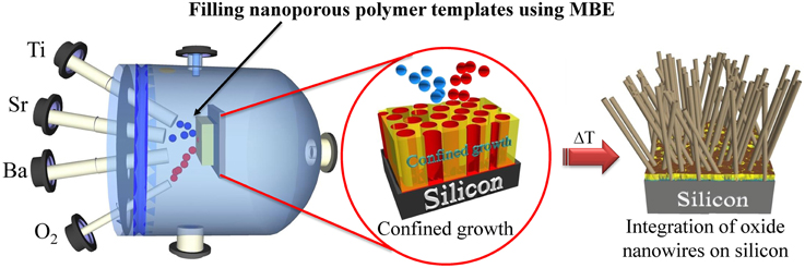
Figure 7. Scheme of an O-MBE setup that shows the epitaxial integration of oxides nanowires on silicon through a metallic evaporation under atomic oxygen inside the pores of a supported track etched polymer templates.
Conclusions
Along this review we have provided an overview showing the most successful strategies used to monolithically integrate functional complex oxide thin films and nanostructures on silicon. Importantly, the interplay of parameters such as chemical reactivity, crystallographic structure epitaxial misfit, interface, and surface energies is crucial for the nucleation and the final crystallographic phase stabilization of nanostructures.
A special emphasis has been put on the combination of chemical solutions deposition methodology with physical methods (MBE) in order to obtain novel functional oxide heterostructures on silicon. We have shown the power of coupling solution chemistry and epitaxial growth. This combination of physics, chemistry and processing allows nanostructured, epitaxial crystalline thin films and nanostructures. As an example, we have presented the integration of LCO thin film by PAD on top of a STO buffer layer grown by MBE.
Another strategy presented in this review, is based on the controlled catalytic devitrification of the silica native layer at the silicon interface which makes possible the integration of novel functional oxide thin films and nanostructures on silicon. In this direction, we have shown in detail the development of nanostructured piezoelectric epitaxial quartz films grown on silicon, and the epitaxial stabilization of complex oxide nanowires with enhanced magnetic properties.
Conflict of Interest Statement
The authors declare that the research was conducted in the absence of any commercial or financial relationships that could be construed as a potential conflict of interest.
Acknowledgments
AC acknowledges the financial support from 1D-RENOX project (Cellule Energie INSIS-CNRS). J.M.V.-F. also acknowledges MINECO for support with a Ph.D. grant of the FPI program. We thank David Montero and L. Picas for technical support. We also thank P. Regreny, C. Botella, J.B. Goure for technical assistance on the Nanolyon technological platform. We acknowledge MICINN (MAT2008-01022 MAT2011-28874-c02-01 and MAT2012-35324), Consolider NANOSELECT (CSD2007-00041), Generalitat de Catalunya (2009 SGR 770 and Xarmae), and EU (HIPERCHEM, NMP4-CT2005-516858) projects. The HAADF-STEM microscopy work was conducted at the Center for Nanophase Materials Sciences, which is a DOE Office of Science User Facility. This research was supported by the European Research Council (ERC StG-2DTHERMS), Ministerio de Economía y Competitividad of Spain (MAT2013-44673-R) and EU funding Project “TIPS” Thermally Integrated Smart Photonics Systems Ref: 644453 call H2020-ICT-2014-1.
Abbreviations
AFM, Atomic Force Microscopy; ALD, Atomic Layer Deposition; BFO, Bismuth Ferrite (BiFeO3); CVD, Chemical Vapor Deposition; CSD, Chemical Solution Deposition; CMOS, Complementary Metal-oxide-semiconductor; EB, Electron-beam; EBDW, Electron-beam Direct Write; EELS, Electron Energy Loss Spectroscopy; EMCD, Electron Magnetic Circular Dichroism; EO, Electro-optic; FE-SEM, Field Emission Scanning Electron Microscopy; HAADF, High-angle annular dark-field; LCO, Lanthanum Cobaltite (LaCoO3); LAO, Lanthanum Aluminate (LaAlO3); MBE, Molecular Beam Epitaxy; MOSFET, Metal-oxide-semiconductor Field-effect transistor; O-MBE, Oxide- molecular beam epitaxy; OMS, Octahedral Molecular Sieve; PLD, Pulsed Laser Deposition; PVD, Physical Vapor Deposition; PFM, Piezoresponce Force Microscopy; PAD, Polymer-assisted deposition; RHEED, Reflection High Energy Electron Diffraction; PZT, Lead Zirconate Titanate (Pb(Zr0.2Ti0.8)O3); PEI, Polyethyleneimine; STO, Strontium Titanate (SrTiO3); STEM, Scanning Transmission Electron Microscopy; TEOS, Tetraethoxysilane; TEM, ransmission Electron Microscopy; UV, Ultraviolet; YSZ, Yttria-stabilized zirconia.
References
1. Wilk GD, Wallace RM, Anthony JM. High-κ gate dielectrics: current status and materials properties considerations. J Appl Phys. (2001) 89:5243–75. doi: 10.1063/1.1361065
2. Guha S, Narayanan V. High-κ/metal gate science and technology. Annu Rev Mater Res. (2009) 39:181–202. doi: 10.1146/annurev-matsci-082908-145320
3. Park JW, Bogorin DF, Cen C, Felker DA, Zhang Y, Nelson CT, et al. Creation of a two-dimensional electron gas at an oxide interface on silicon. Nat Commun. (2010) 1. doi: 10.1039/c3cs60365b
4. Niu G, Yin S, Saint-Girons G, Gautier B, Lecoeur P, Pillard V, et al. Epitaxy of BaTiO3 thin film on Si(001) using a SrTiO3 buffer layer for non-volatile memory application. Microelectron Eng. (2011) 88:1232–5. doi: 10.1016/j.mee.2011.03.028
5. Abel S, Stoferle T, Marchiori C, Rossel C, Rossell MD, Erni R, et al. A strong electro-optically active lead-free ferroelectric integrated on silicon. Nat Commun. (2013) 4:1671. doi: 10.1038/ncomms2695
6. Xiong C, Pernice WH, Ngai JH, Reiner JW, Kumah D, Walker FJ, et al. Active silicon integrated nanophotonics: ferroelectric BaTiO(3) devices. Nano Lett. (2014) 14:1419–25. doi: 10.1021/nl404513p
7. Schlom DG, Chen LQ, Pan X, Schmehl A, Zurbuchen MA. A thin film approach to engineering functionality into oxides. J Am Ceramic Soc. (2008) 91:2429–54. doi: 10.1111/j.1551-2916.2008.02556.x
8. Herklotz A, Dörr K, Ward TZ, Eres G, Christen HM, Biegalski MD. Stoichiometry control of complex oxides by sequential pulsed-laser deposition from binary-oxide targets. Appl Phys Lett. (2015) 106:131601. doi: 10.1063/1.4916948
9. Dave HAB, Matthijn D, Guus R. Pulsed laser deposition in twente: from research tool towards industrial deposition. J Phys D Appl Phys. (2014) 47:034006. doi: 10.1088/0022-3727/47/3/034006
10. Musil J, Baroch P, Vlèek J, Nam KH, Han JG. Reactive magnetron sputtering of thin films: present status and trends. Thin Solid Films (2005) 475:208–18. doi: 10.1016/j.tsf.2004.07.041
11. Pervez NK, Hansen PJ, York RA. High tunability barium strontium titanate thin films for rf circuit applications. Appl Phys Lett. (2004) 85:4451–53. doi: 10.1063/1.1818724
13. Schlom DG, Haeni JH, Lettieri J, Theis CD, Tian W, Jiang JC, et al. Oxide nano-engineering using MBE. Mater Sci Eng B (2001) 87:282–91. doi: 10.1016/S0921-5107(01)00726-7
14. Liang Y, Kulik J, Eschrich TC, Droopad R, Yu Z, Maniar P. Hetero-epitaxy of perovskite oxides on GaAs(001) by molecular beam epitaxy. Appl Phys Lett. (2004) 85:1217–9. doi: 10.1063/1.1783016
15. Merckling C, Saint-Girons G, Botella C, Hollinger G, Heyns M, Dekoster J, et al. Molecular beam epitaxial growth of BaTiO3 single crystal on Ge-on-Si(001) substrates. Appl Phys Lett. (2011) 98:092901. doi: 10.1063/1.3558997
16. Louahadj L, Le Bourdais D, Largeau L, Agnus G, Mazet L, Bachelet R, et al. Ferroelectric Pb(Zr,Ti)O3 epitaxial layers on GaAs. Appl Phys Lett. (2013) 103:212901. doi: 10.1063/1.4831738
17. Laha A, Bugiel E, Osten HJ, Fissel A. Crystalline ternary rare earth oxide with capacitance equivalent thickness below 1nm for high-k application. Appl Phys Lett. (2006) 88. doi: 10.1063/1.2198518
18. Bachelet R, De Coux P, Warot-Fonrose B, Skumryev V, Niu G, Vilquin B, et al. Functional spinel oxide heterostructures on silicon. Cryst Eng Comm. (2014) 16:10741–5. doi: 10.1039/C4CE01817F
19. McKee RA, Walker FJ, Chisholm MF. Crystalline oxides on silicon: the first five monolayers. Phys Rev Lett. (1998) 81:3014–17. doi: 10.1103/PhysRevLett.81.3014
20. Martin LW, Chu YH, Ramesh R. Advances in the growth and characterization of magnetic, ferroelectric, and multiferroic oxide thin films. Mater Sci Eng R Rep. (2010) 68:89–133. doi: 10.1016/j.mser.2010.03.001
21. McKee RA, Walker FJ, Nardelli MB, Shelton WA, Stocks GM. The interface phase and the Schottky barrier for a crystalline dielectric on silicon. Science (2003) 300:1726–30. doi: 10.1126/science.1083894
22. Reiner JW, Kolpak AM, Segal Y, Garrity KF, Ismail-Beigi S, Ahn CH, et al. Crystalline oxides on silicon. Adv Mater Weinheim. (2010) 22:2919–38. doi: 10.1002/adma.200904306
23. Sambri A, Gariglio S, Torres Pardo A, Triscone JM, Stéphan O, Reiner JW, et al. Enhanced critical temperature in epitaxial ferroelectric Pb(Zr0.2Ti0.8)O3 thin films on silicon. Appl Phys Lett. (2011) 98:012903. doi: 10.1063/1.3532110
24. Baek SH, Eom CB. Epitaxial integration of perovskite-based multifunctional oxides on silicon. Acta Mater. (2013) 61:2734–50. doi: 10.1016/j.actamat.2012.09.073
25. Demkov AA, Posadas AB, Seo H, Choi M, Kormondy KJ, Ponath P, et al. (Invited) monolithic integration of oxides on semiconductors. ECS Trans. (2013) 54:255–69. doi: 10.1149/05401.0255ecst
26. Dubourdieu C, Bruley J, Arruda TM, Posadas A, Jordan-Sweet J, Frank MM, et al. Switching of ferroelectric polarization in epitaxial BaTiO3 films on silicon without a conducting bottom electrode. Nat Nano (2013). 8:881. doi: 10.1038/nnano.2013.226
27. Fork DK, Fenner DB, Connell GAN, Phillips JM, Geballe TH. Epitaxial yttria−stabilized zirconia on hydrogen−terminated Si by pulsed laser deposition. Appl Phys Lett. (1990) 57:1137–9. doi: 10.1063/1.104220
28. Bachelet R, De Coux P, Warot-Fonrose B, Skumryev V, Fontcuberta J, Sánchez F. CoFe2O4/buffer layer ultrathin heterostructures on Si(001). J Appl Phys. (2011) 110:086102. doi: 10.1063/1.3651386
29. Scigaj M, Dix N, Fina I, Bachelet R, Warot-Fonrose B, Fontcuberta J, et al. Ultra-flat BaTiO3 epitaxial films on Si(001) with large out-of-plane polarization. Appl Phys Lett. (2013) 102:112905. doi: 10.1063/1.4798246
30. Xiu-Tian Y, Yongdong X. Chemical Vapour Deposition: An Integrated Engineering Design for Advanced Materials. England: Springer London Ltd. (2012).
31. Leskelä M, Ritala M. Atomic layer deposition (ALD): from precursors to thin film structures. Thin Solid Films (2002) 409:138–146. doi: 10.1016/S0040-6090(02)00117-7
32. George SM. Atomic layer deposition: an overview. Chem Rev. (2010) 110:111–31. doi: 10.1021/cr900056b
33. Jeffrey Brinker C, Scherer GW. Sol-Gel Science: The Physics and Chemistry of Sol-Gel Processing. San Diego, CA: Gulf Professional Publishing (1990).
34. Jia QX, McCleskey TM, Burrell AK, Lin Y, Collis GE, Wang H, et al. Polymer-assisted deposition of metal-oxide films. Nat Mater. (2004) 3:529–32. doi: 10.1038/nmat1163
36. Narayanan M, Schwartz RW. “Chemical Solution Deposition–BasicPrinciples,” In: Mitzi DB, editor. Solution-Based Processing of Inorganic Materials. Hoboken, NJ: John Wiley & Sons, Inc (2008). p. 53–96.
37. Schneller T, Waser R, Kosec M, Payne D. (2013). Chemical Solution Deposition of Functional Oxide Thin Films. Heidelberg; New York, NY; Dordrecht; London: Springer Wien.
38. Calzada ML, Gonzalez A, Poyato R, Pardo L. Photo-sensitive sol-gel solutions for the low-temperature UV-assisted processing of PbTiO3 based ferroelectric thin films. J Mater Chem. (2003). 13:1451–7. doi: 10.1039/b300036m
39. Calzada ML, Bretos I, Jiménez R, Guillon H, Pardo L. Low-temperature processing of ferroelectric thin films compatible with silicon integrated circuit technology. Adv Mater. (2004) 16:1620–4. doi: 10.1002/adma.200306401
40. Wu A, Vilarinho PM, Reaney I, Miranda Salvado IM. Early stages of crystallization of sol-gel-derived lead zirconate titanate thin films. Chem Mater. (2003) 15:1147–55. doi: 10.1021/cm020757k
41. Bretos I, Jiménez R, Wu A, Kingon AI, Vilarinho PM, Calzada ML. Activated solutions enabling low-temperature processing of functional ferroelectric oxides for flexible electronics. Adv Mater. (2014) 26:1405–9. doi: 10.1002/adma.201304308
42. De Dobbelaere C, Calzada ML, Jiménez R, Ricote J, Bretos I, Mullens J, et al. Aqueous solutions for low-temperature photoannealing of functional oxide films: reaching the 400°C si-technology integration barrier. J Am Chem Soc. (2011) 133:12922–5. doi: 10.1021/ja203553n
43. Gutiérrez-Lázaro C, Bretos I, Jiménez R, Ricote J, Hosiny HE, Pérez-Mezcua D, et al. Solution synthesis of BiFeO3 thin films onto silicon substrates with ferroelectric, magnetic, and optical functionalities. J Am Ceram Soc. (2013) 96:3061–69. doi: 10.1111/jace.12569
44. Hu C, McDaniel MD, Posadas A, Demkov AA, Ekerdt JG, Yu ET. Highly controllable and stable quantized conductance and resistive switching mechanism in single-crystal TiO2 resistive memory on silicon. Nano Lett. (2014) 14:4360–7. doi: 10.1021/nl501249q
45. McDaniel MD, Ngo TQ, Posadas A, Hu C, Lu S, Smith DJ, et al. A chemical route to monolithic integration of crystalline oxides on semiconductors. Adv Mater Interfaces (2014) 1:1400081. doi: 10.1002/admi.201400081
46. McDaniel MD, Posadas A, Ngo TQ, Dhamdhere A, Smith DJ, Demkov AA, et al. Growth of epitaxial oxides on silicon using atomic layer deposition: crystallization and annealing of TiO2 on SrTiO3-buffered Si(001). J Vac Sci Technol B (2012) 30:04E111-1–6. doi: 10.1116/1.4734311
47. McDaniel MD, Posadas A, Ngo TQ, Dhamdhere A, Smith DJ, Demkov AA, et al. Epitaxial strontium titanate films grown by atomic layer deposition on SrTiO3-buffered Si(001) substrates. J Vac Sci Technol A (2013) 31:01A136-1–9. doi: 10.1116/1.4770291
48. Ngo TQ, Posadas A, McDaniel MD, Ferrer DA, Bruley J, Breslin C, et al. Epitaxial growth of LaAlO3 on SrTiO3-buffered Si (001) substrates by atomic layer deposition. J. Cryst. Growth (2013) 363:150–7. doi: 10.1016/j.jcrysgro.2012.10.032
49. Ngo TQ, Posadas AB, McDaniel MD, Hu C, Bruley J, Yu ET, et al. Epitaxial c-axis oriented BaTiO3 thin films on SrTiO3-buffered Si(001) by atomic layer deposition. Appl Phys Lett. (2014) 104:082910. doi: 10.1063/1.4867469
50. Vila-Fungueiriño JM, Rivas-Murias B, Rodríguez-González B, Rivadulla F. Interface magnetic coupling in epitaxial bilayers of La0.92MnO3/LaCoO3 prepared by polymer-assisted deposition. Chem Mater. (2014) 26:1480–4. doi: 10.1021/cm403868y
51. Brezesinski T, Groenewolt M, Gibaud A, Pinna N, Antonietti M, Smarsly B. Evaporation-induced self-assembly (EISA) at its limit: ultrathin, crystalline patterns by templating of micellar monolayers. Adv Mater. (2006) 18:2260–3. doi: 10.1002/adma.200600258
52. Sanchez C, Boissiere C, Cassaignon S, Chaneac C, Durupthy O, Faustini M, et al. Molecular engineering of functional inorganic and hybrid materials. Chem Mater. (2013) 26:221–38. doi: 10.1021/cm402528b
53. Carretero-Genevrier A, Drisko GL, Grosso D, Boissiere C, Sanchez C. Mesoscopically structured nanocrystalline metal oxide thin films. Nanoscale (2014a) 6:14025–43. doi: 10.1039/C4NR02909G
54. Alexe M, Hesse D. Self-assembled nanoscale ferroelectrics. J Mater Sci. (2006) 41:1–11. doi: 10.1007/s10853-005-5912-x
55. Obradors X, Puig T, Gibert M, Queralto A, Zabaleta J, Mestres N. Chemical solution route to self-assembled epitaxial oxide nanostructures. Chem Soc Rev. (2014) 43:2200–25. doi: 10.1039/c3cs60365b
56. Martin CR. Nanomaterials: a membrane-based synthetic approach. Science (1994) 266:1961–6. doi: 10.1126/science.266.5193.1961
57. Lee T, Yao N, Aksay IA. Nanoscale patterning of barium titanate on block copolymers. Langmuir (1997) 13:3866–70. doi: 10.1021/la960774m
58. Luo Y, Szafraniak I, Zakharov ND, Nagarajan V, Steinhart M, Wehrspohn RB, et al. Nanoshell tubes of ferroelectric lead zirconate titanate and barium titanate. Appl Phys Lett. (2003) 83:440–2. doi: 10.1063/1.1592013
59. Carretero-Genevrier A, Gázquez J, Puig T, Mestres N, Sandiumenge F, Obradors X, et al. Vertical nanostructures: vertical (La,Sr)MnO3 nanorods from track-etched polymers directly buffering substrates (Adv. Funct. Mater. 6/2010). Adv Funct Mater. (2010) 20:892–7. doi: 10.1002/adfm.201090015
60. Carretero-Genevrier A, Gazquez J, Magen C, Varela M, Ferain E, Puig T, et al. Chemical synthesis of oriented ferromagnetic LaSr-2 x 4 manganese oxide molecular sieve nanowires. Chem Commun. (2012) 48:6223–5. doi: 10.1039/c2cc31367g
61. Zhu XH, Evans PR, Byrne D, Schilling A, Douglas C, Pollard RJ, et al. Perovskite lead zirconium titanate nanorings: towards nanoscale ferroelectric “solenoids”? Appl Phys Lett. (2006) 89:122913–5. doi: 10.1063/1.2347893
62. Kim S, Bastani Y, Lu H, King WP, Marder S, Sandhage KH, et al. Direct fabrication of arbitrary-shaped ferroelectric nanostructures on plastic, glass, and silicon substrates. Adv Mater. (2011) 23:3786–90. doi: 10.1002/adma.201190130
63. Alexe M, Harnagea C, Hesse D, Gösele U. (1999). Patterning and switching of nanosize ferroelectric memory cells. Appl Phys Lett. 75:1793–5. doi: 10.1063/1.124822
64. Chih-Min C, Ming-Chung W, Yu-Ching H, Kuo-Chung C, Ching-Fu L, Yang-Fang C, et al. Nanolithography made from water-based spin-coatable LSMO resist. Nanotechnology (2006) 17:4399. doi: 10.1088/0957-4484/17/17/019
65. Carretero-Genevrier A, Gich M, Picas L, Gazquez J, Drisko GL, Boissiere C, et al. Soft-chemistry-based routes to epitaxial alpha-quartz thin films with tunable textures. Science (2013a) 340:827–31. doi: 10.1126/science.1232968
66. Matusita K, Tashiro M. Rate of homogeneous nucleation in alkali disilicate glasses. J Non-Crystalline Solids (1973) 11:471–84. doi: 10.1016/0022-3093(73)90092-6
67. Drisko GL, Carretero-Genevrier A, Gich M, Gàzquez J, Ferrah D, Grosso D, et al. Water-induced phase separation forming macrostructured epitaxial quartz films on silicon. Adv Funct Mater. (2014) 24:5494–502. doi: 10.1002/adfm.201401066
68. Carretero-Genevrier A, Gich M, Picas L, Sanchez C, Rodriguez-Carvajal J. FD Nucleation: chiral habit selection on nanostructured epitaxial quartz films. Faraday Discuss. (2015). doi: 10.1039/C4FD00266K
69. Carretero-Genevrier A, Puig T, Obradors X, Mestres N. Ferromagnetic 1D oxide nanostructures grown from chemical solutions in confined geometries. Chem Soc Rev. (2014b) 43:2042–54. doi: 10.1039/C3CS60288E
70. Carretero-Genevrier A, Oro-Sole J, Gazquez J, Magén C, Miranda L, Puig T, et al. Direct monolithic integration of vertical single crystalline octahedral molecular sieve nanowires on silicon. Chem Mater. (2013b) 26:1019–28. doi: 10.1021/cm403064u
71. Carretero-Genevrier A, Gazquez J, Idrobo JC, Oro J, Arbiol J, Varela M, et al. Single crystalline La0.7Sr0.3MnO3 molecular sieve nanowires with high temperature ferromagnetism. J Am Chem Soc. (2011) 133:4053–61. doi: 10.1021/ja1098963
72. Carretero-Genevrier A, Mestres N, Puig T, Hassini A, Oró J, Pomar A, et al. Single-crystalline La0.7Sr0.3MnO3 nanowires by polymer-template-directed chemical solution synthesis. Adv Mater. (2008) 20:3672–7. doi: 10.1002/adma.200800487
73. Gazquez J, Carretero-Genevrier A, Gich M, Mestres N, Varela M. Electronic and magnetic structure of LaSr-2x4 manganese oxide molecular sieve nanowires. Microsc Microanal. (2014) 20:760–6. doi: 10.1017/S1431927614000592
74. Schattschneider P, Rubino S, Hebert C, Rusz J, Kunes J, Novák P, et al. Detection of magnetic circular dichroism using a transmission electron microscope. Nature (2006) 441:486–8. doi: 10.1038/nature04778
75. Luo W, Varela M, Tao J, Pennycook SJ, Pantelides ST. Electronic and crystal-field effects in the fine structure of electron energy-loss spectra of manganites. Phys Rev B (2009) 79:052405. doi: 10.1103/PhysRevB.79.052405
Keywords: epitaxial growth, silicon, solution chemistry, quartz
Citation: Vila-Fungueiriño JM, Bachelet R, Saint-Girons G, Gendry M, Gich M, Gazquez J, Ferain E, Rivadulla F, Rodriguez-Carvajal J, Mestres N and Carretero-Genevrier A (2015) Integration of functional complex oxide nanomaterials on silicon. Front. Phys. 3:38. doi: 10.3389/fphy.2015.00038
Received: 05 March 2015; Accepted: 15 May 2015;
Published: 09 June 2015.
Edited by:
Zorica Konstantinovic, Institute of Material Science of Barcelona, SpainReviewed by:
Christos Dimitrakopoulos, University of Massachusetts, Amherst, USAJeffry Kelber, University of North Texas, USA
Copyright © 2015 Vila-Fungueiriño, Bachelet, Saint-Girons, Gendry, Gich, Gazquez, Ferain, Rivadulla, Rodriguez-Carvajal, Mestres and Carretero-Genevrier. This is an open-access article distributed under the terms of the Creative Commons Attribution License (CC BY). The use, distribution or reproduction in other forums is permitted, provided the original author(s) or licensor are credited and that the original publication in this journal is cited, in accordance with accepted academic practice. No use, distribution or reproduction is permitted which does not comply with these terms.
*Correspondence: Adrián Carretero-Genevrier, Institut des Nanotechnologies de Lyon, Centre National de la Recherche Scientifique - École Centrale de Lyon, 36 Avenue Guy de Collongue, 69134 Lyon, France, carreterogenevrier@gmail.com