Control of Magnetism in Dilute Magnetic Semiconductor (Ga,Mn)As Films by Surface Decoration of Molecules
 Hailong Wang
 Xiaolei Wang1
  Jianhua Zhao
- 1State Key Laboratory of Superlattices and Microstructures, Institute of Semiconductors, Chinese Academy of Sciences, Beijing, China
- 2Department of Physics, Florida State University, Tallahassee, FL, USA
The responses of magnetic moments to external stimuli such as magnetic-field, heat, light, and electric-field have been utilized to manipulate the magnetism in magnetic semiconductors, with many of the novel ideas applied even to ferromagnetic metals. Here, we review a new experimental development on the control of magnetism in (Ga,Mn)As thin films by surface decoration of organic molecules: Molecules deposited on the surface of (Ga,Mn)As thin films are shown to be capable of significantly modulating their saturation magnetization and Curie temperature. These phenomena are shown to originate from the carrier-mediated ferromagnetism in (Ga,Mn)As and the surface molecules acting as acceptors or donors depending on their highest occupied molecular orbitals, resembling the charge transfer mechanism in a pn junction in which the equilibrium state is reached on the alignment of Fermi levels.
Introduction
Magnetic materials have been an integral part of modern daily lives, used extensively in applications such as magnetic hard drives and random access memories, where the spontaneous magnetization is used to store information [1]. The basic functions of a memory element involve read and write operations; the former can be accomplished nearly non-dissipatively by exploiting the giant/tunneling magneto-resistance (GMR/TMR) effect [2–5]. However, much more energy is needed for the write operation, namely, for switching the magnetization direction of the magnetic bit [6]. Conventionally, a magnetic field generated by an electric current is used to change the magnetization direction, inevitably leading to unwanted power dissipation in the form of the Joule heat [7]. In addition, the non-local nature of a magnetic field also severely restricts the miniaturization of the magnetic memory devices [8]. This problem can be circumvented by the so-called spin-torque technique, now widely employed in the non-volatile magnetic random access memory (MRAM), in which the magnetization reversal is induced by a torque carried by a spin-polarized current exerting on the magnetic moment [7–9]. However, the required critical current density is still too large to efficiently decrease the energy consumption [7–10].
Moreover, considering the stability of the magnetic information storage, the magnetic bits should be essentially immune to ambient fluctuations, which is usually realized by using hard magnets featuring large coercive fields [11]. Hence, to decrease the writing power, one natural idea is to decrease the coercive field momentarily during writing by heat. Note that this method is different from the magnetic-field or spin-torque induced magnetization reversal, since in the latter two cases the magnetic properties can be regarded as unchanged in the process. Based on this idea, heat-assisted magnetic recording (HAMR) technology has been under rapid development in recent years, and is expected to increase the limit of magnetic recording dramatically [12, 13]. However, the high density integration of the heating assemblies remains a great challenge, which involves attaching and aligning a semiconductor diode laser to the write head and implementing near-field optics to deliver the heat at nanoscale [13].
Along the basic idea of HAMR, an attractive alternative involves modulating the magnetic properties temporarily and reversibly, but at ambient temperature. One scheme uses electric-field which holds the advantages of controlling carrier distributions effectively and with high spatial and temporal resolution by consuming nearly negligible power. Although electric-field control of magnetism has been observed in multiferroics [14–16], it is thought very difficult, if not impossible, to realize similar modulation in a magnet. This is attributed to the fact that the electric-field and magnetization do not exhibit direct and strong correlations as in multiferroics. The discovery of carrier-mediated ferromagnetism in (III,Mn)V dilute magnetic semiconductor (DMS) presents an ideal materials system for examining electric-field control of magnetism. In fact, isothermal manipulation of magnetic properties including Curie temperature (TC) and coercive field by electric-field was soon successfully demonstrated in (In,Mn)As films [17]. Later, electric-field assisted magnetization reversal at constant external magnetic field was also realized in (In,Mn)As films, which was made possible by the electric-field control of coercive field [18]. Notice that it is not possible to reverse the magnetization solely by an electric-field, since an electric-field does not cause time-reversal symmetry breaking, which is required during the magnetization reversal process [19, 20]. Thus, an external perturbation such as magnetic field is needed to make one of the bistable states energetically more favorable [19, 20]. Furthermore, as a direct consequence of gate-voltage control of the magnetic anisotropy, it was found that the magnetization direction in (Ga,Mn)As films could also be changed by a gate electric-field, providing an alternative method to the electrical switching of magnetization [21]. The main obstacle for the practical applications of III-V DMS remains the low Curie temperatures, with the record sticking at about 200 K for (Ga,Mn)As nanowires [22]. For this reason, similar schemes were attempted on ultrathin ferromagnetic metal films at room temperature, despite persisting doubts on whether the tiny signal could be observed/exploited [23]. After the first breakthrough on the electric-field control of coercive field in FePd and FePt thin films by using ionic liquid to generate a giant interfacial electric-field [24], much progress has been achieved in recent years, such as the electrical control of magnetic anisotropy, coercive field, and even TC in Fe, CoFeB, and Co thin films [25–32]. More intriguing, electrical switching of FeCo and CoFeB ultrathin films in magnetic tunnel junctions (MTJs) has also been realized, laying the groundwork for their potential applications in MRAM [33–38]. For more details about the electric-field effects on magnetism in metals, the readers can refer to several recent review papers [19, 37–39]. Besides, combining the ferroelectric and ferromagnetic materials in a heterostructure, non-volatile electric-field control of magnetism in (Ga,Mn)As has also been demonstrated [40]. In addition to the electrical methods, it was found that the magnetism could be tuned by photo-illumination in magnetic semiconductor systems, exemplified by (In,Mn)As/GaSb heterostructures and (Cd,Mn)Te quantum wells [41, 42]. These phenomena are also related to the modulation of carrier density, but controlled by photo-excitation.
Although the application of DMSs is limited due to their low TC, many novel ideas and results extracted from research on DMS have inspired further work in many ferromagnetic metals now used in practical devices [19, 33–39]. For example, the gate voltage-controlled magnetic anisotropy first demonstrated in DMS [17, 18, 21] was utilized in ferromagnetic metal based MTJs [33–39]. On the other hand, it continues to be of fundamental interest to explore new means and examine the extent of tuning the magnetism reversibly with minimal changes in temperature. From this point of view, DMSs still serve as an ideal system for testing new ideas and studying physical mechanisms. For instance, the ferromagnet-molecule interface has been the focus of many recent studies [43, 44], due to their novel electrical and magnetic functionalities. Spin-filtering effect and large spin polarization at the interface of ferromagnetic metals and nonmagnetic organic molecules have been revealed both by theoretical calculations [44, 45] and experiments [44, 46, 47]. Interfacial magnetization in the organic molecules may also be induced [48] and the surface magnetic anisotropy of the ferromagnetic metal be modified [49]. Even more intriguing, induced magnetization on the surfaces of nonmagnetic metals through decoration of organic self-assembled monolayers (SAMs) [46, 50] has been demonstrated, which parallels another hot topic in the electric-field creation of magnetism in nonmagnetic metals [51]. In this review article, we focus on the recent developments on the control of magnetism in DMS (Ga,Mn)As films by taking advantages of the diverse functionalities of organic molecules.
Surface Decoration of Organic Molecules on (Ga,Mn)As Films
Both electron donor and acceptor molecules were used to decorate the surface of (Ga,Mn)As films. The electron donor molecule was chosen to be a thiol molecule, 16-mercaptohexadecanoic acid (MHA). A schematic representation of the molecular structure of MHA with the passivation and MHA assembly procedures on (Ga,Mn)As is shown in Figure 1A. The as-grown film was first immersed in an ammonium sulfide solution, which etches away the native oxide and forms a sulfur passivation layer on the sample surface. The sulfur passivation protects the sample from re-oxidation and facilitates the final MHA monolayer molecule self-assembly. The preparation of a properly passivated oxide-free (Ga,Mn)As surface was found to be the key step for the realization of the high-quality MHA self-assembled monolayer on (Ga,Mn)As [52, 53]. The effects of the sulfur-passivation and formation of MHA SAM on the treated surface had been confirmed by high-resolution transmission electron microscopy, dip-pen nanolithography (DPN), and X-ray photoelectron spectroscopy (XPS) [54].
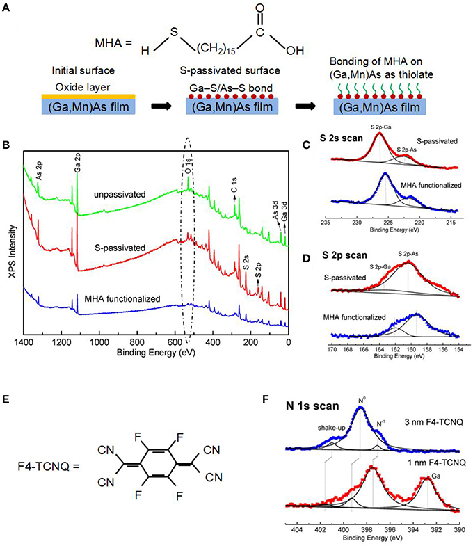
Figure 1. Surface decoration of electron donor and acceptor organic molecules on (Ga,Mn)As films [54]. (A) Schematic representation of the surface modification procedures for MHA SAM. (B) XPS spectra of unpassivated, S-passivated, and MHA-functionalized GaAs samples. (C) Enlarged XPS spectra for sulfur 2s, which show two peaks (corresponding to S 2s-Ga and S 2s-As respectively). (D) Magnified XPS spectra for sulfur 2p, in which both the traces of S 2p-Ga and S 2p-As can be observed. (E) Molecular structure of F4-TCNQ. (F) The XPS spectra of N 1s core level for 1 nm monolayer and 3 nm multilayer F4-TCNQ on (Ga,Mn)As films, revealing the saturation effect of the charge transfer process.
Figure 1B shows the XPS scans of three semi-insulating GaAs samples which had been stored in air for several months. The first sample was measured as-cleaved (green curve), the second sample was immersed in a diluted 1% (NH4)2S solution (red curve), and the third sample was both immersed in a diluted (NH4)2S solution and a 1 mM MHA ethanol solution (blue curve). All the samples were then exposed to the air again for several days, after which XPS measurements were carried out. Clear signatures of oxidation (i.e., O 1s core level peaks) on the native surface were observed for the unpassivated sample, in contrast to the S-passivated and MHA-functionalized samples. The enlarged sulfur 2s and 2p XPS spectra were shown in Figures 1C,D, both the S 2s and 2p peaks showed two peaks corresponding to Ga-S and As-S bonding present at the surface. The absence of spectral features at binding energy (BE) ≥ 163.5 eV in the S 2p region indicated that there were no free thiol groups in these films, which was consistent with the S-passivation and thiol binding. Both the S 2s and S 2p peaks of MHA-functionalized samples shifted to lower energies compared to the S-passivated samples, implying successful replacement of the S by the thiol in MHA. Other features such as Ga 3d, As 2p, and 3d as well as the C 1s spectra also strongly suggested the successful S-passivation and the replacement of S by the thiol in MHA [54–56]. Further evidences of the MHA SAM assembly on the S-passivated (Ga,Mn)As surfaces include the successful DPN nanoscale patterning, as shown in reference [54].
To accumulate holes in the (Ga,Mn)As layer, molecules with strong electron affinity should be utilized. Here, 2,3,5,6-tetrafluoro-7,7,8,8-tetracyanoquinodimethane (F4-TCNQ) with molecular structure depicted in Figure 1E was used to increase the hole density in the (Ga,Mn)As film. In fact, it had already been shown in various p- or n-type materials that the adsorption of F4-TCNQ led to strong compensation of electrons [57–60]. It was thus expected that F4-TCNQ thermally evaporated on the surface would inject holes into (Ga,Mn)As, in spite of its degenerate p-type characteristic.
Extensive XPS measurements on (Ga,Mn)As films covered with 0, 1, and 3 monolayers of F4-TCNQ on the surface verified the acceptor role of F4-TCNQ. Figure 1F showed XPS results of several characteristic peaks of (Ga,Mn)As films with 1 nm (monolayer) and 3 nm (multilayer) thick F4-TCNQ. The two peaks in the N 1s core-level spectra, which were absent in the as-grown sample, were assigned to the anionic N−1 and neutral N0 species in the molecular layer and the interface. The appearance of the N−1 anion species indicated that the electron transfer took place through the C ≡ N groups of the molecules [58, 60]. It was evident that in these samples, not all C ≡ N groups were involved in the charge transfer process, especially in the one with thicker F4-TCNQ. For monolayer molecular coverage (1 nm), the N−1 species dominated while for thicker F4-TCNQ (3 nm), the neutral N0 carried more spectral weight, likely due to unreacted C ≡ N groups in the upper part of the F4-TCNQ film. In addition, a peak around 393 eV consistent with the Ga LMM Auger peak [61] was present in the 1 nm sample but absent in the 3 nm sample. These results showed that the N−1 spectral feature were contributed by the Ga-N bonds at the interface. The hole injected into the (Ga,Mn)As films was attributed to the alignment of Fermi energy of (Ga,Mn)As with the highest occupied molecular orbital (HOMO) of F4-TCNQ [58, 60, 62], resulting in electrons transferred from the (Ga,Mn)As film to F4-TCNQ.
Modulation of Magnetism in (Ga,Mn)As Films by Organic Molecules
With the molecular decoration of MHA and F4-TCNQ described in the previous section, the effects of carrier doping and modulation of ferromagnetism in (Ga,Mn)As films covered by organic molecules were probed by a combination of magneto-transport and magnetic measurements on the same samples. In order to minimize potential spurious effects from unintended surface contamination/reaction, (Ga,Mn)As films with GaAs cap layers up to 2 nm thick were also grown. The comparison of results with samples without a GaAs cap layer only showed very little difference. Besides, the possible existence of small defects in the organic layers had also been shown to have negligible effect on the modulation of magnetism in (Ga,Mn)As. This was supported by the observation that increasing the immersion time in the MHA solution beyond 1 min and depositing more than 1 nm of F4-TCNQ had no measurable effect on the TC modulation magnitude.
Figure 2 shows the measurement results of a 9 nm thick epitaxial (Ga,Mn)As film capped with a 1 nm GaAs layer. The M(T) data (Figure 2A) reveal clear changes of TC resulting from the surface molecule coverages: the F4-TCNQ enhances TC, while the MHA reduces TC. Quantitatively, TC was determined from the peak temperature of dM/dT, as shown in the inset. M(H) measurements at 5 K with magnetic field applied along GaAs [-110] direction (Figure 2B) revealed a similar trend in the saturation magnetization (MS), which decreased with MHA assembly and increased upon F4-TCNQ deposition on the surface. At the same time, a clearly change of the carrier concentration with the same changing direction could also be observed from the temperature dependent longitudinal resistivity curves, as shown in Figure 2C. Furthermore, the TC estimated from the peaks of these curves also showed similar changing trends with the above magnetic measurement results. To quantitatively determine the carrier concentration, the magnetic field dependence of the Hall resistivity had been measured and presented in Figure 2D. At low field region, the Hall resistivity was mainly contributed by the anomalous Hall component. Again, due to the changing of longitudinal resistivity, the anomalous Hall resistivity also varied accordingly. At high field region, the curve showed mostly the feature of ordinary Hall effect and a linear fitting gave a hole density of 8.9 × 1020 cm−3 for the as-grown sample, which increased (decreased) to 1.45 × 1021 cm−3 (1.35 × 1020 cm−3) with the deposition of F4-TCNQ (MHA). The correlation between the resistivity and hole concentration was qualitatively in consistent with previous works [63–65].
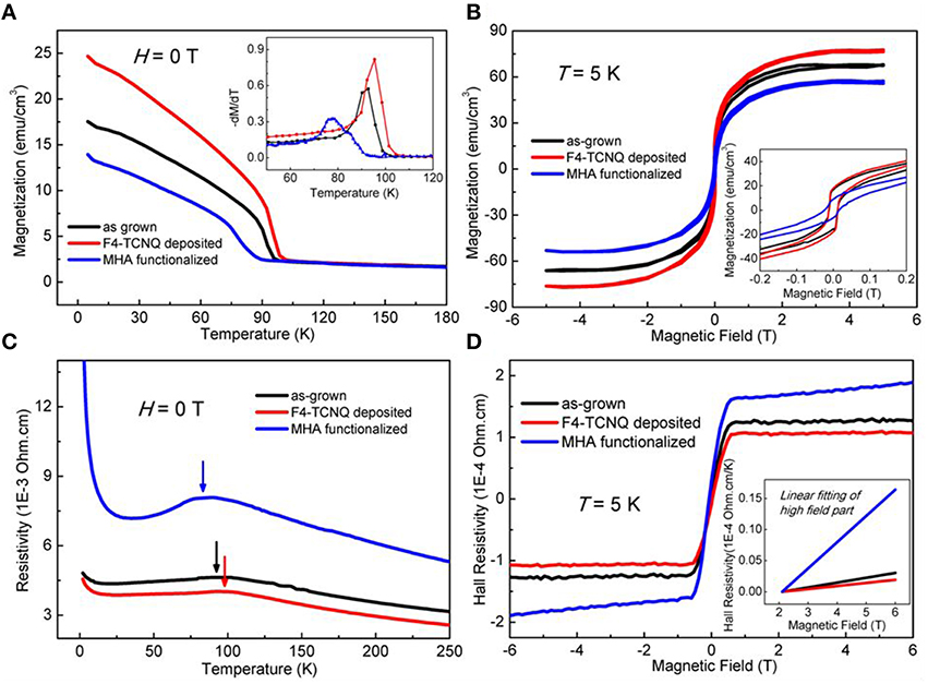
Figure 2. Molecular modifications of ferromagnetism in a 9 nm thick (Ga,Mn)As film capped with 1 nm GaAs [54]. (A) Temperature dependence of the remnant magnetization M(T). Inset: temperature derivative of the remnant magnetization dM/dT vs. temperature curves, showing more clearly the modulation of TC for the three films. (B) Magnetization hysteresis loops measured at 5 K for the same three films. Inset: magnification of the low field region. (C) Temperature dependence of the longitudinal resistivity. (D) Hall resistivity for the same three films measured at 5 K. Inset: Linear fittings of the high field data, indicating a clear change of the hole concentrations.
In order to obtain a quantitative and systematic understanding of the mechanism of the molecular modulation of the magnetism in the (Ga,Mn)As films, similar measurements have also been performed for a series of (Ga,Mn)As films with different film and cap layer thicknesses [54]. The nominal Mn concentration of these (Ga,Mn)As films were kept at about 4%. Theoretically, the p-d Zener model for ferromagnetism in DMSs predicts that TC correlates hole concentration in a power form with the exponent γ between 0.6 ~ 0.8 in the relevant range of hole densities [65, 66]. However, for thin films (< 5 nm) in the parallel capacitor structure, the exponents were found to be ~0.2. The much smaller critical exponent was explained by considering the non-uniform distribution of the hole concentration in thin films [67]. In our experiments, γ values much smaller than the prediction in (Ga,Mn)As bulks were also observed in sample with the largest TC modulation up to 36 K, which could also be explained by the modified p-d Zener model [54, 67].
Using molecules to control magnetism of magnetic films is easy to operate experimentally, it is also very convenient to verify the modulation effect: one simply deposits a thin layer of molecules on a large piece of magnetic film, and then the variation of magnetism can be quantitatively determined by a magnetometer, in contrast to indirect characterization methods such as anomalous Hall effect. More importantly, this novel method also enables one to make a very small device, even down to nanoscale [54]. However, effective characterization of the variation of a ferromagnet in nanoscale needs further effort. In addition, it is also very interesting to do the similar experiments on ultrathin magnetic metals, one step further to the possible application of molecules/magnet hybrid structures.
Conclusions
In this article, we review several methods for the control of magnetism and describe results from one that utilizes surface molecular decoration. Organic molecules acting as electron acceptors or donors have been employed to modulate the ferromagnetism in the DMS (Ga,Mn)As films without elevating the sample temperature. The basic mechanism for the magnetism modulation is shown to be the variation of the carrier density in (Ga,Mn)As attributed to the charge transfer with the surface adsorbed molecules. These experimental results provide a novel pathway for reconfigurable and flexible nanoscale control of magnetism utilizing nano-patterns of organic molecules, which may have potential applications in magnetic storage and molecular spintronic devices. This convenient method may be extended to the isothermal control of magnetism in thin ferromagnetic metal films in practical device structures.
Author Contributions
JZ and PX conceived the project presented in this mini review article, XW and HW performed the experiments. HW prepared the manuscript with inputs and revisions from all the authors.
Conflict of Interest Statement
The authors declare that the research was conducted in the absence of any commercial or financial relationships that could be construed as a potential conflict of interest.
Acknowledgments
This work is supported by MOST of China (Grant No. 2013CB922303) and NSFC (Grants No. 61334006 and No. 11404323). Work at FSU is supported by NSF DMR Grant No. 1308613.
References
1. Brataas A, Hals KMD. Spin-orbit torques in action. Nat Nanotechnol. (2014) 9:86–8. doi: 10.1038/nnano.2011.8
2. Fert A. Origin, development and future of spintronics. Rev Mod Phys. (2008) 80:1517–30. doi: 10.1103/RevModPhys.80.1517
3. Grunberg PA. From spin waves to giant magnetoresistance and beyond. Rev Mod Phys. (2008) 80:1531–40. doi: 10.1103/RevModPhys.80.1531
4. Moodera JS, Kinder LR, Wong TM, Meservey R. Large magnetoresistance at room temperature in ferromagnetic thin film tunnel junctions. Phys Rev Lett. (1995) 74:3273–76. doi: 10.1103/PhysRevLett.74.3273
5. Miyazaki T, Tezuka N. Giant magnetic tunneling effect in Fe/Al2O3/Fe junction. J Magn Magn Mater. (1995) 139:L231–34. doi: 10.1016/0304-8853(95)90001-2
6. Parkin SSP, Hayashi M, Thomas L. Magnetic domain-wall racetrack memory. Science (2008) 320:190–4. doi: 10.1126/science.1145799
7. Brataas A, Kent AD, Ohno H. Current-induced torques in magnetic materials. Nat Mater. (2012) 11:372–81. doi: 10.1038/nmat3311
8. Myers EB, Ralph DC, Katine JA, Louie RN, Buhrman RA. Current-induced switching of domains in magnetic multilayer devices. Science (1999) 285:867–70. doi: 10.1126/science.285.5429.867
9. Miron IM, Gaudin G, Auffret S, Rodmacq B, Schuhl A, Pizzini S, et al. Current-driven spin torque induced by the Rashba effect in a ferromagnetic metal layer. Nat Mater. (2010) 9:230–4. doi: 10.1038/nmat2613
10. Locatelli N, Cros V, Grollier J. Spin-torque building blocks. Nat Mater. (2014) 13:11–20. doi: 10.1038/nmat3823
11. Weller D, Moser A. Thermal effect limits in ultra high-density magnetic recording. IEEE Trans Magn. (1999) 35:4423–39. doi: 10.1109/20.809134
12. O'Connor D, Zayats AV. The third plasmonic revolution. Nat Nanotechnol. (2010) 5:482–3. doi: 10.1038/nnano.2010.137
13. Challener WA, Peng C, Itagi AV, Karns D, Peng W, Peng YG, et al. Hear-assisted magnetic recording by a near-field transducer with efficient optical energy transfer. Nat Photon. (2009) 3:220–4. doi: 10.1038/nphoton.2009.26
14. Wang J, Neaton JB, Zheng H, Nagarajan V, Ogale SB, Liu B, et al. Epitaxial BiFeO3 multiferroic thin film heterostructures. Science (2003) 299:1719–22. doi: 10.1126/science.1080615
15. Tokura Y. Multiferroics - toward strong coupling between magnetization and polarization in a solid. J Magn Magn Mater. (2007) 310:1145–50. doi: 10.1016/j.jmmm.2006.11.198
16. Heron JT, Trassin M, Ashraf K, Gajek M, He Q, Yang SY, et al. Electric-field-induced magnetization reversal in a ferromagnet-multiferroic heterostructure. Phys Rev Lett. (2011) 107:217202. doi: 10.1103/PhysRevLett.107.217202
17. Ohno H, Chiba D, Matsukura F, Omiya T, Abe E, Dietl T, et al. Electric-field control of ferromagnetism. Nature (2000) 408:944–6. doi: 10.1038/35050040
18. Chiba D, Yamanouchi M, Matsukura F, Ohno H. Electrical manipulation of magnetization reversal in a ferromagnetic semiconductor. Science (2003) 301:943–5. doi: 10.1126/science.1086608
19. Matsukura F, Tokura Y, Ohno H. Control of magnetism by electric fields. Nat Nanotechnol. (2015) 10:209–20. doi: 10.1038/nnano.2015.22
20. Pantel D, Goetze S, Hesse D, Alexe M. Reversible electrical switching of spin polarization in multiferroic tunnel junction. Nat Mater. (2012) 11:289–93. doi: 10.1038/nmat3254
21. Chiba D, Sawicki M, Nishitani Y, Nakatani Y, Matsukura F, Ohno H. Magnetization vector manipulation by electric fields. Nature (2008) 455:515–8. doi: 10.1038/nature07318
22. Chen L, Yang X, Yang FH, Zhao JH, Misuracea J, Xiong P, et al. Enhancing the Curie temperature of ferromagnetic semiconductor (Ga,Mn)As to 200 K via nanostructure engineering. Nano Lett. (2011) 11:2584–89. doi: 10.1021/nl201187m
24. Weisheit M, Fahler S, Marty A, Souche Y, Poinsignon C, Givord D. Electric field-induced modification of magnetism in thin-film ferromagnets. Science (2007) 315:349–51. doi: 10.1126/science.1136629
25. Maruyama T, Shiota Y, Nozaki T, Ohta K, Toda N, Mizuguchi M, et al. Large voltage-induced magnetic anisotropy change in a few atomic layers of iron. Nat Nanotech. (2009) 4:158–61. doi: 10.1038/nnano.2008.406
26. Endo M, Kanai S, Ikeda S, Matsukura F, Ohno H. Electric-field effects on thickness dependent magnetic anisotropy of sputtered MgO/CoFeB/Ta structures. Appl Phys Lett. (2010) 96:212503. doi: 10.1063/1.3429592
27. Chiba D, Fukami S, Shimamura K, Ishiwata N, Kobayashi K, Ono T. Electrical control of the ferromagnetic phase transition in cobalt at room temperature. Nat Mater. (2011) 10:853–6. doi: 10.1038/nmat3130
28. Shimamura K, Chiba D, Ono S, Fukami S, Ishiwata N, Kawaguchi M, et al. Electrical control of Curie temperature in cobalt using ionic liquid film. Appl Phys Lett. (2012) 100:122402. doi: 10.1063/1.3695160
29. Shiota Y, Bonell F, Miwa S, Mizuochi N, Shinjo T, Suzuki Y. Opposite signs of voltage-induced perpendicular magnetic anisotropy change in CoFeB|MgO junctions with different underlayers. Appl Phys Lett. (2013) 103:082410. doi: 10.1063/1.4819199
30. Koyama T, Obinata A, Hibino Y, Chiba D. Sign reversal of electric field effect on coercivity in MgO/Co/Pt system. Appl Phys Express (2013) 6:123001. doi: 10.7567/APEX.6.123001
31. Bonell F, Takahashi YT, Lam DD, Yoshida S, Shiota Y, Miwa S, et al. Reversible change in the oxidation state and magnetic circular dichroism of Fe driven by an electric field at the FeCo/MgO interface. Appl Phys Lett. (2013) 102:152401. doi: 10.1063/1.4802030
32. Miwa S, Matsuda K, Tanaka K, Kotani Y, Goto M, Nakamura T, et al. Voltage-controlled magnetic anisotropy in Fe|MgO tunnel junction studied by x-ray absorption spectroscopy. Appl Phys Lett. (2015) 107:162402. doi: 10.1063/1.4934568
33. Shiota Y, Nozaki T, Bonell F, Murakami S, Shinjo T, Suzuki Y. Induction of coherent magnetization switching in a few atomic layers of FeCo using voltage pulse. Nat Mater. (2012) 11:39–43. doi: 10.1038/nmat3172
34. Wang WG, Li M, Hageman S, Chien CL. Electric-field-assisted switching in magnetic tunnel junctions. Nat Mater. (2012) 11:64–8. doi: 10.1038/nmat3171
35. Kanai S, Yamanouchi M, Ikeda S, Nakatani Y, Matsukura F, Ohno H. Electric field-induced magnetization reversal in a perpendicular-anisotropy CoFeB-MgO magnetic tunnel junction. Appl Phys Lett. (2012) 101:122403. doi: 10.1063/1.4753816
36. Kanai S, Nakatani Y, Yamanouchi M, Ikeda S, Matsukura F, Ohno H. In-plane magnetic field dependence of electric field-induced magnetization switching. Appl Phys Lett. (2013) 103:072408. doi: 10.1063/1.4818676
37. Wang WG, Chien CL. Voltage-induced switching in magnetic tunnel junctions with perpendicular magnetic anisotropy. J Phys D Appl Phys. (2013) 46:074004. doi: 10.1088/0022-3727/46/7/074004
38. Chiba D, Ono T. Control of magnetism in Co by an electric field. J Phys D Appl Phys. (2013) 46:213001. doi: 10.1088/0022-3727/46/21/213001
39. Chiba D. Electric field effect on magnetism in metallic ultra-thin films. Front Phys. (2015) 3:00083. doi: 10.3389/fphys.2015.00083
40. Stolichnov I, Riester SWE, Trodahl HJ, Setter N, Rushforth AW, Edmonds KW, et al. Non-volatile ferroelectric control of ferromagnetism in (Ga,Mn)As. Nat Mater. (2008) 7:464–7. doi: 10.1038/nmat2185
41. Koshihara S, Oiwa A, Hirasawa M, Katsumoto S, Iye Y, Urano C, et al. Ferromagnetic order induced by photogenerated carriers in magnetic III-V semiconductor heterostructures of (In,Mn)As/GaSb. Phys Rev Lett. (1997) 78:4617–20. doi: 10.1103/PhysRevLett.78.4617
42. Boukari H, Kossacki P, Bertolini M, Ferrand D, Cibert J, Tatarenko S, et al. Light and electric field control of ferromagnetism in magnetic quantum structures. Phys Rev Lett. (2002) 88:207204. doi: 10.1103/PhysRevLett.88.207204
43. Steil S, Grobmann N, Laux M, Ruffing A, Steil D, Wiesenmayer M, et al. Spin-dependent trapping of electrons at spinterface. Nat Phys. (2013) 9:242–7. doi: 10.1038/nphys2548
44. Atodiresei N, Brede J, Lazic P, Caciuc V, Hoffmann G, Wiesendanger R, et al. Design of the local spin polarization at the organic-ferromagnetic interface. Phys Rev Lett. (2010) 105:066601. doi: 10.1103/PhysRevLett.105.066601
45. Herrmann C, Solomon GC, Ratner MA. Organic radicals as spin filters. J Am Chem Soc. (2010) 132:3682–84. doi: 10.1021/ja910483b
46. Gohler B, Hamelbeck V, Markus TZ, Kettner M, Hanne GF, Vager Z et al. Spin selectivity in electron transmission through self-assembled monolayers of double-standarded DNA. Science (2011) 331:894–7. doi: 10.1126/science.1199339
47. Dor OB, Yochelis S, Mathew SP, Naaman R, Paltiel Y. A chiral-based magnetic memory device without a permanent magnet. Nat Commun. (2013) 4:2256. doi: 10.1038/ncomms3256
48. Raman KV, Kamerbeek AM, Mukherjee A, Atodiresei N, Sen TK, Lazic P et al. Interface-engineered templates for molecular spin memory devices. Nature (2013) 493:509–13. doi: 10.1038/nature11719
49. Callsen M, Caciuc V, Kiselev N, Atodiresei N, and Blugel S. Magnetic hardening induced by nonmagnetic organic molecules. Phys Rev Lett. (2013) 111:106805. doi: 10.1103/PhysRevLett.111.106805
50. Ray SG, Daube SS, Leitus G, Vager Z, Naaman R. Chirality-induced spin-selective properties of self-assembled monolayers of DNA on Gold. Phys Rev Lett. (2006) 96:036101. doi: 10.1103/PhysRevLett.96.036101
51. Shimizu S, Takahashi KS, Hatano T, Kawasaki M, Tokura Y, Iwasa Y. Electrically tunable anomalous Hall effect in Pt thin films. Phys Rev Lett. (2013) 111:216803. doi: 10.1103/PhysRevLett.111.216803
52. Petrovykh DY, Yang MJ, Whitman LJ. Chemical and electronic properties of sulfur-passivated InAs surfaces. Surf Sci. (2003) 523:231. doi: 10.1016/S0039-6028(02)02411-1
53. Sourribes MJL, Isakov I, Panfilova M, Warburton PA. Minimization of the contact resistance between InAs nanowires and metallic contacts. Nanotech. (2013) 24:045703. doi: 10.1088/0957-4484/24/4/045703
54. Wang XL, Wang HL, Pan D, Keiper T, Li LX, Yu XZ, et al. Robust manipulation of magnetism in dilute magnetic semiconductor (Ga,Mn)As by organic molecules. Adv Mater. (2015) 27:8043–50. doi: 10.1002/adma.201503547
55. Budz HA, Biesinger MC, LaPierre RR. Passivation of GaAs by octadecanethiol self-assembled monolayers deposited from liquid and vapor phases. J Vac Sci Technol B. (2009) 27:637–48. doi: 10.1116/1.3100266
56. Stine R, Petrovykh DY. Oriented self-assembled monolayers of bifunctional molecules on InAs. J Electron Spectrosc Relat Phenom. (2009) 172:42–6. doi: 10.1016/j.elspec.2009.02.001
57. Takenobu T, Takano T, Shiraishi M, Murakami Y, Ata M, Kataura H, et al. Stable and controlled amphoteric doping by encapsulation of organic molecules inside carbon nanotubes. Nat Mater. (2003) 2:683–8. doi: 10.1038/nmat976
58. Koch N, Duhm S, Rabe JR, Vollmer A, Johnson RL. Optimized hole injection with strong electron acceptors at organic-metal interfaces. Phys Rev Lett. (2005) 95:237601. doi: 10.1103/PhysRevLett.95.237601
59. Kim D, Cho S, Butch NP, Syers P, Kirshenbaum K, Adam S, et al. Surface conduction of topological Dirac electrons in bulk insulating Bi2Se3. Nat Phys. (2012) 8:459–63. doi: 10.1038/nphys2286
60. Coletti C, Riedl C, Lee DS, Krauss B, Patthey L, von Klitzing K, et al. Charge neutrality and band-gap tuning of epitaxial graphene on SiC by molecular doping. Phys Rev B. (2010) 81:235401. doi: 10.1103/PhysRevB.81.235401
61. Wagner CD, Riggs WM, Davis LE, Moulder JF, Muilenberg GE. Handbook of X-Ray Photoelectron Spectroscopy. Eden Prairie, MN: Perkin-Elmer Corporation (1979).
62. Yang HH, Chu YH, Lu CI, Yang TH, Yang KJ, Kaun CC, et al. Digitized charge transfer magnitude determined by metal-organic coordination number. ACS Nano. (2013) 7:2814–9. doi: 10.1021/nn4003715
63. Sawicki M, Chiba D, Korbecka A, Nishitani Y, Majewski JA, Matsukura F, et al. Experimental probing of the interplay between ferromagnetism and localization in (Ga,Mn)As. Nat Phys. (2010) 6:22–5. doi: 10.1038/nphys1455
64. Mayer MA, Stone PR, Miller N, Smith III HM, Dubon OD, Haller EE, et al. Electronic structure of Ga1−xMnxAs analyzed according to hole concentration dependent measurements. Phys Rev B (2010) 81:045205. doi: 10.1103/PhysRevB.81.045205
65. Dietl T, Ohno H, Matsukura F, Cibert J, Ferrand D. Zener model description of ferromagnetism in zinc-blende magnetic semiconductors. Science (2000) 287:1019–22. doi: 10.1126/science.287.5455.1019
66. Dietl T, Ohno H, Matsukura F. Hole-mediated ferromagnetism in tetrahedrally coordinated semiconductors. Phys Rev B (2001) 63:195205. doi: 10.1103/PhysRevB.63.195205
Keywords: molecular control of magnetism, dilute magnetic semiconductors, molecular decoration, carrier-mediated ferromagnetism, highest occupied molecular orbital
Citation: Wang H, Wang X, Xiong P and Zhao J (2016) Control of Magnetism in Dilute Magnetic Semiconductor (Ga,Mn)As Films by Surface Decoration of Molecules. Front. Phys. 4:9. doi: 10.3389/fphy.2016.00009
Received: 28 January 2016; Accepted: 10 March 2016;
Published: 30 March 2016.
Edited by:
Serban Lepadatu, University of Central Lancashire, UKReviewed by:
Sean Langridge, Science and Technology Facilities Council, UKDong-Hyun Kim, Chungbuk National University, South Korea
Copyright © 2016 Wang, Wang, Xiong and Zhao. This is an open-access article distributed under the terms of the Creative Commons Attribution License (CC BY). The use, distribution or reproduction in other forums is permitted, provided the original author(s) or licensor are credited and that the original publication in this journal is cited, in accordance with accepted academic practice. No use, distribution or reproduction is permitted which does not comply with these terms.
*Correspondence: Jianhua Zhao, jhzhao@red.semi.ac.cn