Oxide Single-Crystal Surfaces: A Playground for Self-assembled Oxide Nanostructures
 Romain Bachelet
- Institut des Nanotechnologies de Lyon, Centre National de la Recherche Scientifique - UMR 5270, École Centrale de Lyon, Ecully, France
The different (structural and chemical) properties of oxide single-crystal surfaces that can be exploited for the growth of self-assembled oxide nanostructures are briefly reviewed. A large variety of nanostructures can be obtained, controlled by surface and interface structure and chemistry, which play a predominant role in their formation mechanisms at this nanometer scale. It is reminded that surface atomic order, surface steps, chemical terminations or heteroepitaxial strain can be used to generate various nanostructures such as nanodots, nanowires, nanostripes, with controlled size, morphology, and spatial ordering.
Introduction
Oxides present a wide range of remarkable properties (from metal-insulator transitions to multiferroïcity) that lead to various competing devices such as sensitive sensors, non-volatile memories, low consumption transistors, energy harvesters, and transducers, etc. [1]. Functional oxide nanostructures can even exhibit enhanced or novel physical properties compared to their bulk counterparts, and are thus of great interest for future devices in various application fields. The ability to generate and control different nanostructures (even more complex) would lead to a larger range of physical properties, with a fine understanding of the correlations between the structures at the atomic and nanometer scale and their properties being a key point. Since applications mainly require integration of single-crystalline materials in thin film form, the progress in the elaboration and characterization techniques of epitaxial thin films and supported nanostructures, has been done and has allowed designing materials with an atomic-scale control. Although nanostructures can be designed by top-down approaches (e.g., [2–4]), its high cost and size limitations (~100 nm) have made the low-cost bottom-up approaches involving self-organization processes attractive. This approach is still investigated, as confirmed by the numerous recent papers and the recent issue of MRS Bulletin dedicated to the fabrication of ordered patterns and nanostructures via self-organization [5]. However, the realization of oxide nanostructures is still much less advanced than metal and semiconductor nanostructures, certainly because of the structural and chemical complexity of functional oxides. This complexity of oxides may be an advantage, leading to a larger range of structural/chemical/electronic flexibility and accessible properties, with respect to metals and semiconductors. Indeed, the rich variety of iono-covalent complex oxide structures allows various surface and nanostructure self-assembling properties. The range of available mismatched oxide epitaxial heterostructures is wider than metals and semiconductors and that can therefore lead to many nanostructures through the modulation of interface structure and energy. The nanostructures formation through interface energy modulation is governed by many parameters in dissimilar structures such as the structural mismatch with the most favorable coincident site lattices (CSL), the epitaxial elastic strain, the plastic relaxation created by misfit-accommodation dislocations, with domain matching epitaxy (DME) reducing the global mismatch when the accommodation dislocations are periodic [6–8]. The 3D island growth relieved by epitaxial strain is scarcely observed in oxides in comparison to metals or semiconductors, such as the archetype case of Si1−xGex growth on Si (001) surface [9, 10], probably because of the larger elastic constants in oxides compared to Si and III-V semiconductors (at least by a factor of two). The strain-relieved formation of 3D oxide epitaxial islands has been observed only very low-nanoscale islands (lower than ~100 nm in diameter and a few nanometers in height) [7, 11, 12]. The formation of other nanostructures should be explained by more complex mechanisms taking into account all the above mentioned parameters, the structural anisotropy (driving diffusion anisotropy), the chemical ordering and stoechiometry, surface polarity, and the balance between thermodynamics and kinetic driven by diffusion to flux ratio (D/F) during growth [13–15]. For instance, crystallization annealing of lattice mismatched oxides deposited by chemical solution (CSD) can lead to the formation of epitaxial nanoislands by solid state dewetting where the size, shape, and spatial ordering can be controlled through self-patterning [7, 12, 16–18]. It is also worth noting that some oxide nanocomposites of different structures can be formed by self-assembly through spinodal decomposition mechanisms, as the artificial multiferroic nanocomposites composed of a ferromagnetic spinel and ferroelectric perovskite [19–23]. Stencil masks or nanoporous polymeric layers can also be used as templates for the realization of periodic arrays of functional oxide nanodots or nanowires [3, 24–26]. Another example is the fabrication of oxide-semiconductor core-shell nanowires that can be elaborated by molecular beam epitaxy (MBE) [27]. In addition to these mechanisms, the chemical termination of single-crystalline perovskite oxide substrates has played a major role in the conducted epitaxial growth of high quality oxide films and nanostructures. The progress made to control the chemical termination by chemical and thermal treatments of the most used oxide single-crystal substrates, SrTiO3(001) in particular [28, 29], has opened doors toward the control, enhancement and emergence of original physical properties [30–32], with the most famous example of the formation of a high-mobility two-dimension electron gas (2DEG) at the LaAlO3/SrTiO3 interface appearing only on the TiO2 termination of the SrTiO3 (001) surface [30]. In addition, we will see that self-assembly of the chemical terminations of (001)-oriented perovskite single-crystals can also be used to generate different nanostructures. Here, it will be briefly reviewed how the structural and chemical surface properties of oxide single-crystalline substrates can be used to tailor oxide nanostructures involving some of these self-assembly processes. In particular, it will be enlightened that the atomic structural anisotropy, surface step ordering, self-assembled chemical terminations, and more generally interface energies, are key parameters for the design of nanostructures by preferential atomic diffusion, nucleation and crystallographic orientation. Some examples of nanostructures will be given such as self-organized nanodots, nanowires or nanostripes, with different functional oxides of different structures.
Surface Structure: Anisotropy and Steps
By nature, single-crystalline surfaces are structurally anisotropic due to the specific atomic ordering (see Figure 1A). Atomic rows corresponding to crystallographic directions of low Miller indexes are the most compact and thus with the strongest cohesion energy. This anisotropic atomic ordering of the surface leads to anisotropic atomic surface diffusion, governed by Ehrlich-Schwoebel (ES) barriers [33]. Values of anisotropic diffusion are still unknown, probably because of the structural complexity of oxides. However, the anisotropic diffusion is revealed by epitaxial growth or by annealing single-crystals where faceted edges can be discerned along the crystallographic directions of low Miller indexes at the surface. Similarly to the 90° atomic step-edges of the well-known Si(001) surface [33], faceted atomic step-edges of hundreds of nanometers can be observed on oxide single-crystal surfaces, such as perovskite SrTiO3(001) [29] and SrTiO3(110) [34], and spinel MgAl2O4(001) [35]. Similarly to surface facets of low energy (low Miller indexes) driven by thermodynamic processes (large D/F), elastic interactions and surface polarity reasons [36, 37], epitaxial nanoislands or nanopits can also exhibit faceted edges from tens to hundreds of nanometers along the low-index crystallographic directions [17, 38]. The shape of the nanoislands (pyramidal, hut, or hexagonal) depends on the crystallographic orientation, symmetry, epitaxial strain, surface energy, polarity, etc. The atomic surface reconstructions, that may depend on the oxygen vacancy ratio (e.g., [36, 39, 40]), can be another key parameter to control, favorizing different nanostructures. These anisotropic surface properties have also be used to favor a lateral growth by preferential coarsening along the low index directions, that can lead to horizontal 1D nanowires assisted by epitaxial strain, as in the case of (011)-oriented fluorite Ce1−xGdxO2−y lateral nanowires grown by CSD on LaAlO3 (001) surface, having dimensions of ~20 nm in width and height and more than 1 μm in length [41]. It is worth noting particular oxide materials with high energy anisotropy for which the growth along one direction is favored, naturally leading to 1D nanostructures, as the case of ZnO [42] and WO3 [43] for instance. The mean surfaces of single-crystals present atomic steps due to inevitable (polar and azimuthal) miscut angles because of the accuracy limitations of sample positioning during its cutting and polishing processes (see Figures 1B,C). The standard single-crystalline substrates have polar miscut angles lower than 0.3°, which corresponds to a unit-cell (uc) step every 75 nm at the SrTiO3(001) surface for instance. Because of available specific substrates with different miscut angles that can be provided (from low 0.1 to 10°), the terrace width can be tuned from ~250 to 2.5 nm. Surface steps are preferential nucleation sites (lowering the local free energy) and are anisotropic barriers for atomic surface diffusion [33]. As the step edges preferentially follow the low-index directions, the stepped surface morphology can be determined by the azimuthal miscut angle. Straight step edges will preferentially form on substrates with an azimuthal miscut angle along a low-index direction whereas “zigzag” steps will form when the azimuthal angle is off-low-index directions [34]. Since surface steps give rise to ES barriers for atomic diffusion, preferential alignment along the steps of epitaxial nanodots of ~50 nm in diameter and less than 10 nm in height has been grown by preferential diffusion along the steps [44]. Also, as the surface atomic steps have an energetic cost (lower coordination sites), they will preferentially assemble together when the atomic surface diffusion will be larger than the mean terrace width, to form well-defined stable higher steps and wider terraces of lower energy (like surface facets of low Miller indexes). Almost-nominal atomically-flat surfaces can then be obtained by annealing on perovskite single-crystals like SrTiO3(001) [29, 45, 46], NdGaO3(001) [47], on sapphire [48], and on spinel MgAl2O4(001) single-crystals [35] for instance. Similarly to semiconducting and metallic single-crystal surfaces, step bunching at oxide single-crystal surfaces can thus occur when increasing the polar miscut angle and/or annealing temperatures, leading to “hill and valley” surface nanostructures with periodicity of ~80 nm and total height difference of ~10 nm [7, 9]. In such a way, well-defined 1D surface nanostructures from faceted 10°-off vicinal α-Al2O3(0001) surfaces have been used for the realization of 1D well-ordered arrays of oxide nanodots of ~35 nm in diameter and ~8 nm in height through preferential 1D atomic surface diffusion in the valleys [7]. In the case of high miscut angles (high density of surface steps) and dissimilar heterostructures, the out-of-plane lattice mismatch existing between the film and a step of the substrate surface can lead to a crystallographic tilt, that can be written as follows: δω = mp.arctan (hf − hs/hs), where mp is the polar miscut angle, hf and hs are the height of the steps of the film and the substrate, respectively [49]. Consequently, the morphology of the nanostructures and in particular the tilt of the crystal and its facets can be controlled by the density of surface steps via the polar miscut angle, as tilted YSZ (002) islands on highly vicinal sapphire surfaces [7, 50].
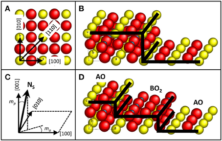
Figure 1. Sketches of oxide single-crystal structure. (A) Sketch of a (001) surface of a perovskite ABO3 single-crystal showing the lowest Miller indexes directions. (B) Sketch of a (001) surface of a perovskite ABO3 single-crystal with an unit-cell high atomic step. (C) Sketch of the polar (mp) and azimuthal (ma) miscut angles, adapted from Bachelet et al. [34]. Ns represents the normal to the mean surface. (D) Sketch of a (001) surface of a perovskite ABO3 single-crystal with a half-unit-cell high atomic step, revealing both alternating chemical terminations AO and BO2.
Surface Chemistry: Atomic Terminations
In addition to structural anisotropy, single-crystal surfaces may have different chemical terminations, as it is the case with the (001)-oriented perovskite surfaces. Because of the inevitable miscut angle and the perovskite ABO3 structure, that can be seen as a periodic stack of AO and BO2 layers in the (001) direction, the epi-polished (001) surfaces of ABO3 single-crystals present both AO and BO2 terminations (see Figure 1D), that have motivated numerous studies from the 90's starting on the SrTiO3 (001) surface with the objective of controlling them for high-quality epitaxial oxide growth and realization of abrupt oxide heterointerfaces [28, 29, 45, 46]. This quest for the control of chemical termination in (001) single-crystal perovskite surfaces has followed with LaAlO3 [47], NdGaO3 [47], LSAT [51], and DyScO3 [52], and on layered SrLaAlO4 substrates [53, 54]. Due to polishing effects, the as-received perovskite substrates have not well-defined step-and-terrace surfaces and contain both chemical terminations, which are mixed at the atomic scale and are difficultly distinguishable by atomic force microscopy (AFM) techniques [55]. Atomic surface diffusion reveals both chemical terminations by self-assembly with well-defined terraces separated by half-uc high steps and terraces of ~150 nm wide depending of the miscut angle and the termination ratio in as-received substrates. This has been observed on SrTiO3 [56], on LaAlO3 [57], on DyScO3 [52], and on LSAT [11]. Surface potential differences between both terminations in SrTiO3 have been predicted to be around 2.3 eV but measured with lower value [32]. These chemically-patterned surfaces have then been used to elaborate different nanostructures by selective growth (see Figure 2). Taking advantage of the termination-dependent chemical or energy properties (hydrophilic SrO termination in SrTiO3 for instance), a selective growth and adsorption of different materials such as SrRuO3, water, and organic tioles has been shown [29, 56, 58]. Ordered 1D nanostructures such as arrays of conducting SrRuO3 nanostripes (of the single-terminated terrace width) or nanodots (~70 nm wide and ~4 nm high) have then been realized in such a way on LaAlO3 [59], SrTiO3 [53, 60], on DyScO3 [52, 61], and on LSAT [11]. In the case of low energy interface, 2D epitaxial growth can occur without preferential nucleation with the chemical terminations replicating themselves at the film surface (see Figure 2A). In addition to the possible modulation of the properties in the out-of-plane direction with layered heterostructures elaborated by advanced deposition techniques, self-assembled chemical terminations have allowed to laterally modulate the interface and surface properties of heterostrucutres [32], generating for instance a 2DEG only at the specific (LaO/TiO2) laterally-confined regions on the single-terminated terrace width of the LaAlO3/SrTiO3 interface [62], as predicted [63]. More generally, that has allowed to study both chemical terminations of various functional perovskite oxides, such as ferromagnetic (La,Sr)MnO3 and ferroelectric BaTiO3, which are difficulty accessible even with advanced and widely used oxide deposition techniques such as pulsed laser deposition (PLD) [32]. The chemical terminations can also have a dramatic effect on the crystallographic orientation and the morphology of thin films, as YSZ on SrTiO3(001) surface where it has been shown that 2D growth of YSZ film only occurs on the SrO termination with (001)-orientation whereas dome-shaped tilted (111)-oriented YSZ islands of a few tens of nanometers in diameter and a few nanometers in height epitaxially grow on the TiO2 termination [64]. This observation has been explained by the differences in terms of chemical bonding and interfacial energies. However, specific energy values for these complex interfaces are tricky to determine and are still unknown.
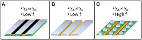
Figure 2. Sketches of the different nanostructures that can be obtained on self-ordered chemical terminations of (001) surface of a perovskite ABO3 single-crystal. f represents the lattice mismatch, γA and γB represent the interfacial energies on AO and BO2 chemical terminations, respectively. (A) Replication of the chemical terminations by 2D growth in case of low interfacial energies and lattice mismatch. (B) Selective 2D growth only on one chemical termination due to different termination-dependent interfacial energies and low lattice mismatch. (C) Selective 3D growth only on one chemical termination due to different termination-dependent interfacial energies and high lattice mismatch.
Interface Structure and Energy
In addition to surface structure and chemistry, interface structure and energy play a particularly important role in the control of the shape of the epitaxial nanoobjects. Lattice mismatch (defined as f = (as − af)/af, where as and af are the in-plane lattice parameter of the substrate and the film, respectively) can generate elastic strain in heteroepitaxial nanostructures. Dissimilar epitaxial structures can thus have different possible structural matching at the interface, with different coincidence site lattices (CSL), and thus different interfacial energies. Epitaxial heterostructures with high interface energy will have tendency to minimize the interface whereas those with low interface energy will have tendency to maximize it [12]. For instance, in the case of dissimilar fluorite (YSZ) on sapphire (0001) surface, two epitaxial orientations can occur: (111) with low interface matching and (001) with domain interface matching reducing the lattice mismatch to 0.9%. It has been observed that for YSZ epitaxial nanoislands grown by CSD, which is a thermodynamically driven growth (very large equivalent D/F), (111)-oriented nanoislands are dome-shaped with minimized interface area and (001)-faceted surfaces, whereas (001)-oriented nanoislands are top-flat with larger interface area, in agreement with their structural matching and expected interface energy [7, 65]. Indeed, it has been shown that the ratio of (111)-oriented dome-shaped nanoislands can be increased by artificially increasing the substrate surface energy, through a soft deterioration of the epi-polished substrate surface done by gentle scratching and further soft annealing leading to an enhancement of the density of surface steps [65]. Another example is the case of the epitaxial growth of SrRuO3 on chemically self-assembled LSAT (001) surface, where a selective growth on only one termination is also observed, similarly to deposition on chemically self-assembled SrTiO3 (001) surface, but forming in that case 1D arrays of nanodots by 3D growth instead of nanostripes by 2D growth (see Figures 2B,C). This difference can be explained by the lattice mismatch that is larger on LSAT (−1.5%) than on SrTiO3 (−0.6%), although the epitaxial strain is in-plane compressive in both cases. The in-plane compressive strain can favor nanoislands formation, whereas in-plane tensile strain can favor nanopits formation, as shown in some epitaxial (La,Sr)MnO3 films grown on SrTiO3 (001) surface by sputtering [66]. Epitaxial growth of films with high surface energy may lead to 3D growth of nanostructures with surface facets of lower energy. That is the case with (001)-oriented spinel films, as ferromagnetic CoFe2O4, that tends to form nanopyramids with more stable (111) facets of lower surface energy at least by a factor of 5 [67, 68]. That is also the case with (110)-oriented perovskite films, such as (La,Sr)MnO3 that tend to form nanohuts with more stable (001) facets [65]. This thermodynamically driven tendency can be kinetically limited by decreasing the D/F ratio, or enhanced by increasing it, tuning the size of the nanoobjects [13, 15, 69].
Conclusions and Prospects
In summary, oxide single-crystal surfaces can be well-exploited for the control of various nanostructures grown by self-assembly processes. We briefly reviewed that the size, shape, and spatial ordering of nanoobjects can be tailored by diverse properties and parameters of oxide single-crystal surfaces such as the structural symmetry, anisotropy and reconstructions, density and morphology of atomic steps tunable by polar and azimuthal miscut angles, chemical terminations that can self-order at the nanoscale, in-plane and out-of-plane lattice mismatches, epitaxial strain, interface energy. Furthermore, the diversity is vast regarding the panoply of elaboration techniques that can be used to drive the growth processes (balanced between thermodynamic and kinetic), leading then to different nanostructures. Novel strategies combining different materials and elaboration techniques can lead to biomimetic hybrid nanostructures with enhanced properties for microfluidic management, sensing, energy conversion, electronic, photonic, biomedical applications [42, 70–73].
Author Contributions
The author confirms being the sole contributor of this work and approved it for publication.
Conflict of Interest Statement
The author declares that the research was conducted in the absence of any commercial or financial relationships that could be construed as a potential conflict of interest.
Acknowledgments
The topic editors are acknowledged for supporting this open-access publication. Flora Blom-Alvarez is gratefully acknowledged for the careful reading of the manuscript.
References
1. Ogale SB (ed.). Thin Films and Heterostructures for Oxide Electronics, New York, NY: Springer (2005).
2. Kim H, Bae C, Jung HS, Lee J-S, Shin H. Direct patterning of metal oxides by hard templates and atomic layer deposition. Int J Nanotechnol. (2010) 10:692–701. doi: 10.1504/IJNT.2013.054211
3. Nijland M, George A, Thomas S, Houwman EP, Xia J, Blank DHA, et al. Patterning of epitaxial perovskite from micro and nano molded stencil masks. Adv Funct Mat (2014) 24:6853–61. doi: 10.1002/adfm.201401170
4. Boes A, Sivan V, Ren G, Yudistira D, Mailis S, Soergel E, et al. Precise, reproductible nano-domain engineering in lithium niobate crystals. Appl Phys Lett. (2015) 107:022901. doi: 10.1063/1.4926910
5. Kang SH, Dickey MD (Guest Editors). Patterning via self-organization and self-folding. MRS Bull. (2016) 41:82–168. doi: 10.1557/mrs.2016.3
6. Narayan J, Larson BC. Domain epitaxy: a unified paradigm for thin film growth. J Appl Phys. (2003) 93:278–85. doi: 10.1063/1.1528301
7. Bachelet R, Cottrino S, Nahélou G, Coudert V, Boulle A, Soulestin B, Rossignol F, et al. Self-patterned oxide nanostructures grown by post-deposition thermal annealing on stepped surfaces. Nanotechnology (2007) 18:015301. doi: 10.1088/0957-4484/18/1/015301
8. Sánchez F, Bachelet R, de Coux P, Warot-Fonrose B, Skumryev V, Tarnawska L, et al. Domain matching epitaxy of ferrimagnetic CoFe2O4 thin films on Sc2O3/Si(111). Appl Phys Lett. (2011) 99:211910. doi: 10.1063/1.3663216
9. Teichert C. Self-organization of nanostructures in semiconductor heteroepitaxy. Phys Reports (2002) 365:335–432. doi: 10.1016/S0370-1573(02)00009-1
10. Shchukin VA, Bimberg D. Spontaneous ordering of nanostructures on crystal surfaces. Reviews Mod Phys. (1999) 71:1125–71. doi: 10.1103/RevModPhys.71.1125
11. Bachelet R, Ocal C, Garzón L, Fontcuberta J, Sánchez F. Conducted growth of SrRuO3 nanodot arrays on self-ordered La0.18Sr0.82Al0.59Ta0.41O3(001) surfaces. Appl Phys Lett. (2011) 99:051914. doi: 10.1063/1.3622140
12. Obradors X, Puig T, Gibert M, Queraltó A, Zabaleta J, Mestres N. Chemical solution route to self-assembled epitaxial oxide nanostructures. Chem Soc Rev. (2014) 43:2200–25. doi: 10.1039/c3cs60365b
13. Barth JV, Costantini G, Kern K. Engineering atomic and molecular nanostructures at surfaces. Nature (2005) 437:671–9. doi: 10.1038/nature04166
14. Hong W, Lee HN, Yoon M, Christen HM, Lowndes DH, Suo Z, et al. Persistent step-flow growth of strained films of vicinal substrates. Phys Rev Lett. (2005) 95:095501. doi: 10.1103/PhysRevLett.95.095501
15. Bachelet R, Pesquera D, Herranz G, Sánchez F, Fontcuberta J. Persistent two-dimensional growth of (110) manganite films. Appl Phys Lett. (2010) 97:121904. doi: 10.1063/1.3490713
16. Lange FF. Chemical solution routes to single-crystal thin films. Science (1996) 273:903–9. doi: 10.1126/science.273.5277.903
17. Langjahr PA, Wagner T, Rühle M, Lange FF. Thermally induced structural changes in epitaxial SrZrO3 films on SrTiO3. J Mater Res. (1999) 14:2945–51. doi: 10.1557/JMR.1999.0394
18. Szafraniak I, Harnagea C, Scholz R, Bhattacharyya S, Hesse D, Alexe M. Ferroelectric epitaxial nanocrystals obtained by a self-patterning method. Appl Phys Lett. (2003) 83:2211. doi: 10.1063/1.1611258
19. Zheng H, Wang J, Lofland SE, Ma Z, Mohaddes-Ardabili L, Zhao T, et al. Multiferroic BaTiO3-CoFe2O4 nanostructures. Science (2004) 303:661–3. doi: 10.1126/science.1094207
20. Zheng H, Zhan Q, Zavaliche F, Sherburne M, Straub F, Cruz MP, et al. Controlling self-assembled perovskite-spinel nanostructures. Nano Lett. (2006) 6:1401–7. doi: 10.1021/nl060401y
21. McManus-Driscoll JL. Self-assembled heteroepitaxial oxide nanocomposite thin film structures: designing interface-induced functionality in electronic materials. Adv Funct Mater. (2010) 20:2035–45. doi: 10.1002/adfm.201000373
22. Chen Y-J, Hsieh Y-H, Liao S-C, Hu Z, Huang M-J, Kuo W-C, et al. Strong magnetic enhancement in self-assembled mutliferroic-ferrimagnetic nanostructures. Nanoscale (2013) 5:4449–53. doi: 10.1039/c3nr00104k
23. Kim DH, Sun XY, Aimon NM, Kim JJ, Campion MJ, Tuller HL, et al. A three component self-assembled epitaxial nanocomposite thin film. Adv Funct Mat. (2015) 25:3091–100. doi: 10.1002/adfm.201500332
24. Vrejoiu I, Alexe M, Hesse D, Gösele U. Functional perovskites - From epitaxial films to nanostructured arrays. Adv Funct Mater. (2008) 18:1–15. doi: 10.1002/adfm.200800560
25. Carretero-Genevrier A, Puig T, Obradors X, Mestres N. Ferromagnetic 1D oxide nanostructures grown from chemical solutions in confined geometries. Chem Soc Rev. (2014) 43:2042–54. doi: 10.1039/c3cs60288e
26. Vila-Fungueirino JM, Bachelet R, Saint-Girons G, Gendry M, Gich M, Gazquez J, et al. Integration of functional complex oxide nanomaterials on silicon. Front Phys. (2015) 3:38. doi: 10.3389/fphy.2015.00038
27. Guan X, Becdelievre J, Meunier B, Benali A, Saint-Girons G, Bachelet R, et al. GaAs core / SrTiO3 shell nanowires grown by molecular beam epitaxy. Nano Lett. (2016) 16:2393–9. doi: 10.1021/acs.nanolett.5b05182
28. Kawasaki M, Takahashi K, Maeda T, Tsuchiya R, Shinohara M, Ishiyama O, et al. Atomic control of the SrTiO3 crystal surface. Science (1994) 266:1540–2. doi: 10.1126/science.266.5190.1540
29. Bachelet R, Sánchez F, Palomares FJ, Ocal C, Fontcuberta J. Atomically flat SrO-terminated SrTiO3(001) substrate. Appl Phys Lett. (2009) 95:141915. doi: 10.1063/1.3240869
30. Ohtomo A, Hwang HY. A high-mobility electron gas at the LaAlO3/SrTiO3 heterointerface. Nature (2004) 427:423–6. doi: 10.1038/nature02308
31. Lu H, Liu X, Burton JD, Bark CW, Wang Y, Zhang Y, et al. Enhancement of ferroelectric polarization stability by interface engineering. Adv Mater. (2012) 24:1209–16. doi: 10.1002/adma.201104398
32. Ocal C, Bachelet R, Garzón L, Stengel M, Sánchez F, Fontcuberta J. Nanoscale laterally modulated properties of oxide ultrathin films by substrate termination replica through layer-by-layer growth. Chem Mater. (2012) 24:4177–84. doi: 10.1021/cm302444s
34. Bachelet R, Valle F, Infante IC, Sánchez F, Fontcuberta J. Step formation, faceting, and bunching in atomically flat SrTiO3(110) surfaces. Appl Phys Lett. (2007) 91:251904. doi: 10.1063/1.2825586
35. Yanina SV, Carter CB. Terraces and ledges on (001) spinel surfaces. Surf Sci. (2002) 513:L402–12. doi: 10.1016/S0039-6028(02)01825-3
36. Noguera C. Polar oxide surfaces. J Phys Cond Matter. (2000) 12:R367–410. doi: 10.1088/0953-8984/12/31/201
37. Goniakowski J, Finocchi F, Noguera C. Polarity of oxide surfaces and nanostructures. Rep Prog Phys. (2008) 71:016501. doi: 10.1088/0034-4885/71/1/016501
38. Konstantinović Z, Sandiumenge F, Santiso J, Balcells L, Martínez B. Self-assembled pit arrays as templates for the integration of Au nanocrystals in oxide surfaces. Nanoscale (2013) 5:1001–8. doi: 10.1039/c2nr33181k
39. Kolpak AM, Li D, Shao R, Rappe AM, Bonnell DA. Evolution of the structure and the thermodynamic of the BaTiO3(001) surface. Phys Rev Lett. (2008) 101:036102. doi: 10.1103/PhysRevLett.101.036102
40. Tselev A, Ganesh P, Qiao L, Siemons W, Gai Z, Biegalski MD, et al. Oxygen control of atomic structure and physical properties of SrRuO3 surfaces. ACS Nano (2013) 7:4403–13. doi: 10.1021/nn400923n
41. Gibert M, Abellán P, Benedetti A, Puig T, Sandiumenge F, García A, et al. Self-organized Ce1−xGdxO2−y nanowire networks with very fast coarsening driven by attractive elastic interactions. Small (2010) 6:2716–24. doi: 10.1002/smll.201001237
42. Yuan W, Lu Z, Li CM. Self-assembling microsized materials to fabricate multifunctional hierarchical nanostructures on macroscale substrates. J Mat Chem A (2013) 1:6416–24. doi: 10.1039/c3ta10704c
43. Vankova S, Zanarini S, Amici J, Camara F, Arletti R, Bodoardo S, et al. WO3 nanorolls self-assembled as thin films by hydrothermal synthesis. Nanoscale (2015) 7:7174–7. doi: 10.1039/c4nr07290a
44. Gibert M, Puig T, Obradors X, Benedetti A, Sandiumenge F, Hühne R. Self-organization of heteroepitaxial CeO2 nanodots grown from chemical solutions. Adv Mater. (2007) 19:3937–42. doi: 10.1002/adma.200700361
45. Koster G, Kropman BL, Rijnders GJHM, Blank DHA. Quasi ideal strontium titanate crystal surfaces through formation of strontium hydroxyde. Appl Phys Lett. (1998) 73:2920–2. doi: 10.1063/1.122630
46. Ohnishi T, Shibuya K, Lippmaa M, Kobayashi D, Kumigashira H, Oshima M, et al. Preparation of thermally stable TiO2-terminated SrTiO3(100) substrate surfaces. Appl Phys Lett. (2004) 85:272–4. doi: 10.1063/1.1771461
47. Ohnishi T, Takahashi K, Nakamura M, Kawasaki M, Yoshimoto M, Koinuma H. A-site layer terminated perovskite substrate: NdGaO3. Appl Phys Lett. (1999) 74:2531. doi: 10.1063/1.123888
48. Yoshimoto M, Maeda T, Ohnishi T, Koinuma H, Ishiyama, Shinohara M, et al. Atomic-scale formation of ultrasmooth surfaces on sapphire substrates for high-quality thin-film fabrication. Appl Phys Lett. (1995) 67:2615–7. doi: 10.1063/1.114313
49. Nagai H. Structure of vapor deposited GaxIn1−xAs crystals. J Appl Phys. (1974) 45:3789. doi: 10.1063/1.1663861
50. Bachelet R, Nahélou G, Boulle A, Guinebretière R, Dauger A. Control of the morphology of oxide nano-islands through the substrate miscut angle. Prog Solid State Chem. (2005) 33:327–32. doi: 10.1016/j.progsolidstchem.2005.11.017
51. Ngai JH, Schwendemann TC, Walker AE, Segal Y, Walker FJ, Altman EI, et al. Achieving A-site termination on La0.18Sr0.82Al0.59Ta0.41O3 substrates. Adv Mater. (2010) 22:2945–8. doi: 10.1002/adma.200904328
52. Kleibeuker JE, Koster G, Siemons W, Dubbink D, Kuiper B, Blok JL, et al. Atomically defined rare-earth scandate crystal surfaces. Adv Funct Mat. (2010) 20:3490–6. doi: 10.1002/adfm.201000889
53. Becerra-Toledo AE, Marks LD. Strontium oxide segregation at SrLaAlO4 surfaces. Surf Sci. (2010) 604:1476–80. doi: 10.1016/j.susc.2010.05.011
54. Biswas A, Rossen PB, Ravichandran J, Chu Y-H, Lee Y-W, Yang C-H, et al. Selective A- or B-site single termination on surfaces of layered oxide SrLaAlO4. Appl Phys Lett. (2013) 102:051603. doi: 10.1063/1.4790575
55. Koster G, Rijnders G, Blank DHA, Rogalla H. Surface morphology determined by (001) single-crystal SrTiO3 termination. Phys C (2000) 339:215–30. doi: 10.1016/S0921-4534(00)00363-4
56. Bachelet R, Sánchez F, Santiso J, Munuera C, Ocal C, Fontcuberta J. Self-assembly of SrTiO3(001) chemical terminations: a route for oxide nanostructure fabrication by selective growth. Chem Mater. (2009) 21:2494–8. doi: 10.1021/cm900540z
57. Gunnarsson R, Kalabukhov AS, Winkler D. Evaluation of recipes for obtaining single terminated perovskite oxide substrates. Surf Sci. (2009) 603:151–7. doi: 10.1016/j.susc.2008.10.045
58. Paradinas M, Garzón L, Sánchez F, Bachelet R, Amabilino DB, Fontcuberta J, et al. Tuning the local frictional and electrostatic responses of nanostructured SrTiO3 surfaces by self-assembled molecular monolayers. Phys Chem Chem Phys. (2010) 12:4452–8. doi: 10.1039/b924227a
59. Vasco E, Dittman R, Karthäuser S, Waser R. Early self-assembled stages in epitaxial SrRuO3 on LaAlO3. Appl Phys Lett. (2003) 82:2497–9. doi: 10.1063/1.1566798
60. He J, Dittman R, Karthäuser S, Vasco E. Geometric shadowing from rippled SrRuO3/SrTiO3 surface templates induces self-organization of epitaxial SrZrO3 nanowires. Phys Rev B (2006) 74:205410. doi: 10.1103/PhysRevB.74.205410
61. Kuiper B, Blok JL, Zandvliet HJW, Blank DHA, Rijnders G, Koster G. Self-organization of SrRuO3 nanowires on ordered oxide surface terminations. MRS Commun. (2011) 1:17–21. doi: 10.1557/mrc.2011.8
62. Foerster M, Bachelet R, Laukhin V, Fontcuberta J, Herranz G, Sánchez F. Laterally confined two-dimensional electron gases in self-patterned LaAlO3/SrTiO3 interfaces. Appl Phys Lett. (2012) 100:231607. doi: 10.1063/1.4728109
63. Bristowe NC, Fix T, Blamire MG, Littlewood PB, Artacho E. Proposal of a one-dimensional electron gas in the steps at the LaAlO3-SrTiO3 interface. Phys Rev Lett. (2012) 108:166802. doi: 10.1103/PhysRevLett.108.166802
64. Cavallaro A, Ballesteros B, Bachelet R, Santiso J. Heteroepitaxial orientation control of YSZ thin films by selective growth on SrO-, TiO2-terminated SrTiO3 crystal surfaces. Cryst Eng Comm. (2011) 13:1625–31. doi: 10.1039/c0ce00606h
65. Bachelet R, Boulle A, Soulestin B, Rossignol F, Guinebretière R, Dauger A. Two-dimensional versus three-dimensional post-deposition grain growth in epitaxial oxide thin films: Influence of the substrate surface roughness. Thin Solid Films (2007) 515:7080–5. doi: 10.1016/j.tsf.2007.02.099
66. Konstantinovic Z, Santiso J, Balcells L, Martínez B. Strain-driven self-assembled network of antidots in complex oxide thin films. Small (2009) 5:265–71. doi: 10.1002/smll.200800814
67. Lüders U, Sánchez F, Fontcuberta J. Self-organized structures in CoCr2O4(001) thin films: tunable growth from pyramidal clusters to a {111} fully faceted surface. Phys Rev B (2004) 70:045403. doi: 10.1103/PhysRevB.70.045403
68. Mishra RK, Thomas G. Surface energy of spinel. J Appl Phys. (1977) 48:4576–80. doi: 10.1063/1.323486
69. Dix N, Fina I, Bachelet R, Fábrega L, Kanamadi C, Fontcuberta J, et al. Large out-of-plane ferroelectric polarization in flat epitaxial BaTiO3 on CoFe2O4 heterostructures. Appl Phys Lett. (2013) 102:172907. doi: 10.1063/1.4803943
70. Huang J, Lai Y, Wang L, Li S, Ge M, Zhang K, et al. Controllable wettability and adhesion on bioinspired multifunctional TiO2 nanostructure surfaces for liquid manipulation. J Mater Chem A (2014) 2:18531–8. doi: 10.1039/c4ta04090b
71. Zhang S, Zhang P, Wang Y, Ma Y, Zhong J, Sun X. Facile fabrication of a well-ordered porous Cu-doped SnO2 thin film for H2S sensing. ACS Appl Mater Interfaces (2014) 6:14975–80. doi: 10.1021/am502671s
72. Kawasaki S, Takahashi R, Yamamoto T, Kobayashi M, Kumigashira H, Yoshinobu J, et al. Photoelectrochemical water splitting enhanced by self-assembled metal nanopillars embedded in oxide semiconductor photoelectrode. Nat Commun. (2016) 7:11818. doi: 10.1038/ncomms11818
Keywords: oxide single-crystals, surface structure and chemistry, self-assembly, nanostructures, interface energy
Citation: Bachelet R (2016) Oxide Single-Crystal Surfaces: A Playground for Self-assembled Oxide Nanostructures. Front. Phys. 4:36. doi: 10.3389/fphy.2016.00036
Received: 30 April 2016; Accepted: 15 August 2016;
Published: 30 August 2016.
Edited by:
Zorica Konstantinovic, Institute of Material Science of Barcelona, SpainReviewed by:
Shikha Varma, Institute of Physics, IndiaHans Boschker, Max Planck Institut für Festkörperforschung, Germany
Copyright © 2016 Bachelet. This is an open-access article distributed under the terms of the Creative Commons Attribution License (CC BY). The use, distribution or reproduction in other forums is permitted, provided the original author(s) or licensor are credited and that the original publication in this journal is cited, in accordance with accepted academic practice. No use, distribution or reproduction is permitted which does not comply with these terms.
*Correspondence: Romain Bachelet, romain.bachelet@ec-lyon.fr