Compact Quantum Random Number Generator with Silicon Nanocrystals Light Emitting Device Coupled to a Silicon Photomultiplier
 Zahra Bisadi1*
  Fabio Acerbi2 Giorgio Fontana1 Nicola Zorzi2 Claudio Piemonte2 Georg Pucker2
  Lorenzo Pavesi1
- 1Nanoscience Laboratory, Department of Physics, University of Trento, Trento, Italy
- 2Center for Materials and Microsystems, Bruno Kessler Foundation (FBK), Trento, Italy
A small-sized photonic quantum random number generator, easy to be implemented in small electronic devices for secure data encryption and other applications, is highly demanding nowadays. Here, we propose a compact configuration with Silicon nanocrystals large area light emitting device (LED) coupled to a Silicon photomultiplier to generate random numbers. The random number generation methodology is based on the photon arrival time and is robust against the non-idealities of the detector and the source of quantum entropy. The raw data show high quality of randomness and pass all the statistical tests in national institute of standards and technology tests (NIST) suite without a post-processing algorithm. The highest bit rate is 0.5 Mbps with the efficiency of 4 bits per detected photon.
1. Introduction
Thanks to the quantum properties of light, “truly” random numbers can be produced by photonic quantum random number generators (PQRNG). Cryptographic tasks of encryption and decryption of private data can be executed using secret keys based on high quality random numbers. Even though mathematical algorithms are extensively used to generate random numbers, they suffer from high guessability provided the seed of the algorithm is known. If they have a short periodicity, their repeatability would be a serious flaw, as well.
PQRNGs benefit from the intrinsically random and unpredictable properties of physical processes involving photons as the quanta of light. The randomness in path taken by photons arriving on a beam splitter1 [1], the comparison of the waiting time for photon arrivals in adjacent time intervals [2] and the combination of both methods [3] have been used to generate random numbers. In some other works, encoding the number of arriving photons in observation windows [4–6] and the randomness in the photon arrival times [7–9] have been used to produce random numbers. Recently, a robust approach based on arrival times of photons has been proposed by our group [9]. It considers all the non-idealities of the source as well as the detector, producing high quality random numbers which pass all the statistical tests in national institute of standards and technology (NIST) tests suite and TestU01 without a post-processing algorithm1.
However, in all the above-mentioned approaches a bulky setup is used to generate random numbers. A small-sized and compact PQRNG, easy to be implemented in small electronic devices such as mobile phones and cameras for secure data encryption and decryption as well as other applications, is highly essential for facile accessibility to everyone. Here, we present a first step toward this goal: a PQRNG with a novel, compact configuration comprising a silicon nanocrystals large area LED (Si-NCs LLED) coupled with a silicon photomultiplier (SiPM) in free space. Based on some statistical analyses described in section 5, it is proved that the generated hexadecimal random symbols have a very high quality and the corresponding random bits pass all the statistical tests in NIST tests suite with no post-processing operations. The highest bit rate of 0.5 Mbps is achieved with the efficiency of 4-bits per detected photon.
In a previous work [9], we have demonstrated a procedure to extract high quality random numbers from the arrival time of photons emitted by a Si-NCs LED, collected by a fiber bundle and detected by a commercial single photon avalanche diode (SPAD). In this work we use the same robust methodology of random number extraction of Bisadi et al. [9] but we demonstrate a PQRNG where the LLED is directly faced to a SiPM. Moreover, both devices are fabricated by the same silicon pilot line of Bruno Kessler Foundation (FBK) with a dimension allowing optimum coupling which is specifically challenging for the Si-NCs LLED.
This work is organized as follows. In section 2, the Si-NCs LLEDs and their electrical and optical characteristics are described. In section 3, the SiPM is introduced and explained. Section 4 describes the experimental procedure and random numbers extraction. Randomness analyses are discussed in section 5 and at the end the conclusions are presented.
2. Si-NCs Large Area LED
Si-NCs are silicon quantum dots which emit light at room temperature in the visible range due to quantum confinement. The emitted photons are emitted independently by a quantum process named spontaneous emission and their statistics obey Poisson statistics (see more in section 4).
Si-NCs LEDs are fabricated by complementary metal-oxide-semiconductor (CMOS) processing, they can be easily incorporated in integrated configurations, they emit photons with wavelengths in the spectral range detectable by silicon detectors allowing the fabrication of an all-silicon-based device and since the spontaneous emission of photons in a Si-NCs LED is a non-deterministic, quantum mechanical and random process, they can be used as a quantum source of randomness to generate random numbers. The Si-NCs LEDs were fabricated with a large emitting surface in order to illuminate large area detectors like the SiPM we use here. The matching of the emitter and detector surfaces allows their direct coupling, i.e., without any coupling optics. The Si-NCs LLED (large area LED) has the active layer structure formed by a multilayer structure with 5 periods of silicon rich oxide (SRO)/SiO2 layers of 3.5–4 nm and 2 nm thicknesses, respectively (Figure 1A). The Si-NCs are grown in a silica matrix through the plasma enhanced chemical vapor deposition (PECVD) technique and annealed at 1150°C for 30 min to form the Si-NCs.
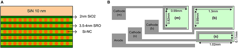
Figure 1. (A) The multilayer structure of Si-NCs LLED with 5 periods of 3.5–4 nm silicon rich oxide (SRO) sandwiched between 2 nm thick SiO2. (B) The geometry of Si-NCs LLED with different sizes b (big), m (medium) and s (small). The cathode and common anode electrodes are shown.
The Si-NCs LLEDs have been prepared in three different sizes: big (b), medium (m) and small (s) with emitting surface area of 1.3 mm × 0.99 mm, 0.99 mm × 0.82 mm and 1.02 mm × 0.11 mm, respectively (see Figure 1B).
The electroluminescence (EL) spectra of the Si-NCs LLEDs can be seen in Figure 2A with a high peak at ~ 900 nm attributed to the emission from Si-NCs. Note that all the LLEDs show the same EL lineshape which points to the great uniformity of the fabrication. Table 1 reports the optoelectronic characteristics of these LLEDs. The figure of merit is the efficiency of the EL which is measured as the ratio between the EL intensity and the driving electrical power. The electrical power density is calculated to be 5.87, 0.93 and 0.08 mW/cm2 for the (b), (m) and (s) LLEDs, respectively. It should be noted that the applied currents to the (b), (m) and (s) LLEDs are 30, 3 and 3 μA, respectively.
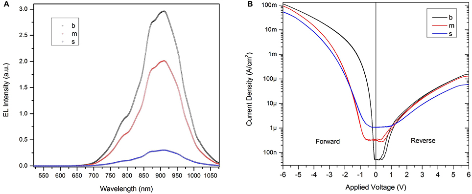
Figure 2. (A) The EL spectra of the three different sizes of Si-NCs LLED illustrated in Figure 1A. A high peak at ~900 nm can be seen which is attributed to the emission from Si-NCs. The EL spectra are acquired by a Spectra-Pro 2300i monochromator coupled with a nitrogen-cooled charge coupled device (CCD) camera. The measurements were performed at room temperature in a dark chamber. EL intensity is normalized for the responsivity of the spectrometer. (B) The I/V characteristics of the Si-NCs LLEDs. A quite rectifying behavior is observed in the I/V curves with more current density at forward regime—i.e., negative voltage applied to the n-type contact electrode and zero voltage to the p-type contact electrode—than reverse regime—i.e., positive voltage applied to the n-type contact electrode and zero voltage to the p-type contact electrode.
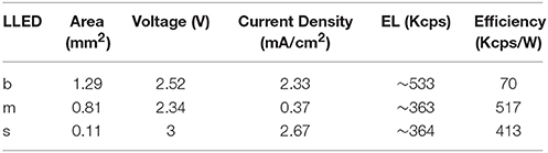
Table 1. The efficiency (EL over injected power) of (b), (m), and (s)LLED.
At currents lower than 30μA to the (b) LLED, no appreciable EL is observed. Therefore, by applying the previously-mentioned currents to the LLEDs, we tried to keep the voltages and hence the electric field through the active area of the LLEDs (with actual thickness of ~22.5 nm) more or less the same. The low current density and high EL intensity of the (m)LLED yield the higher efficiency of this LLED compared with the (b) and (s) LLEDs. In addition to the efficiency, the active area of (m)LLED allows a suitable coupling with the large area SiPM since the SiPM dimensions are of 1 mm × 1 mm. It should be noted that all three LLEDs result in the generation of high quality random numbers since they are fabricated in a very similar way and the detected photons from all of them follow a Poisson distribution.
The current-voltage (I/V) characteristics of Si-NCs LLED are presented in Figure 2B. They show a rectifying behavior with more current density at forward regime—i.e., negative voltage applied to the cathode and zero voltage to the anode—than the reverse regime—i.e., positive voltage applied to the cathode and zero voltage to the anode. It is observed that at a fixed forward voltage, the current density through the (b) LLED is larger than (m) and (s) LLEDs (particularly at 0.5–3 V): this is due to the larger free carrier density flowing through the active area in (b) than (m) and (s) LLEDs. In the reverse bias region (1–6 V), however, the (b), (m), and (s) LLEDs show the same order of magnitude current densities that is related to the inefficient carrier injection to the active area by the accumulation of the charges near the boundaries of the cathode and the anode. This effect blocks the carriers from flowing through, recombining and contributing to the net current and consequently makes the current density independent of the gate areas of the LLEDs2. The charge blocking seems to be more effective for (s) LLED with a flat I/V curve at the region of −0.5–1 V (Figure 2B).
These LLEDs can emit light over long hours of operation. Figure 3 shows the EL of the (m) LLED over ~16 h. Note that the EL variation is compensated by the randomness extraction [9] and does not influence the quality of random numbers and therefore no adjustment of the QRNG is needed over a very long working period.
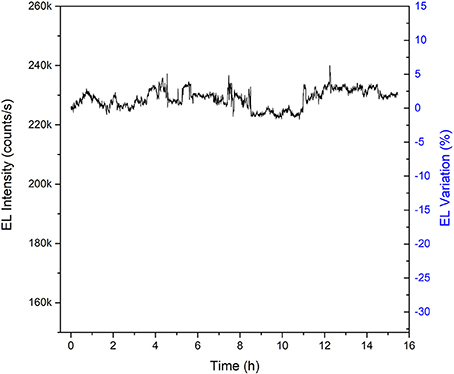
Figure 3. EL of the (m) LLED vs. time at the applied current density of 0.62 mA/cm2 (corresponding to an applied voltage of 2.61 V). The right hand side of the figure (blue axis) shows the EL variation percentage.
3. Silicon Photomultiplier
The analog SiPM is an array of many (hundreds) of single photon avalanche diodes (SPADs). They are all connected in parallel to a common anode and cathode, each one with its own quenching resistor. Each cell (i.e., SPAD+resistor) is sensitive to a single photon and provides a current pulse at the output. Therefore, the counts at the SiPM output are proportional to the number of triggered cells, thus to the number of detected photons. Different technologies for SiPM have been developed in FBK during last few years, with peak sensitivity in the green part (RGB-SiPM) or in the blue part (NUV-SiPM) of the visible spectrum, and with different cell sizes. The NUV technology, in particular, benefits from an upgraded silicon material [10], employing an epi/substrate structure with a lower-lifetime substrate. This gives particular benefits in terms of correlated noise reduction, i.e., afterpulsing probability (AP) and delayed crosstalk probability (DeCT), which are particularly detrimental for QRNG applications [9].
In this work we employ a 1 mm × 1 mm NUV SiPM (inset in Figure 4B), containing 625 cells (SPADs) with the cell size of 40 μm and the fill factor (FF) of 60 %. This particular technology has a photon detection efficiency (PDE) (and in particular spectral sensitivity) not matched to the LLED emission. PDE is about 5% at 800 nm, at 4 V of excess bias (i.e., the difference between the applied bias and the breakdown voltage (Vbd)), as shown in Figure 4A. However, NUV SiPM has the advantage of a low primary dark count rate (DCR), less than 100 kcps/mm2 at 5 V of excess bias (see Figure 4B), meaning less than 200 cps per single SPAD. In addition, it has a reduced correlated noise probability (overall AP+DeCT probability lower than 5%), which is very important in this kind of application.
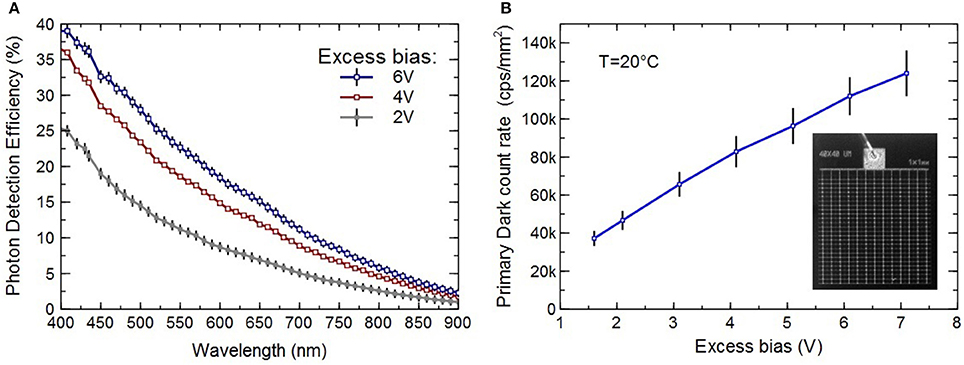
Figure 4. (A) Measured photon detection efficiency (PDE), including the FF, as a function of wavelength for NUV SiPM at excess bias of 2, 4, and 6 V. (B) Dark count rate (DCR) of NUV SiPM vs. excess bias at temperature of 20°C. The inset shows 1 mm × 1 mm SiPM containing 625 SPADs with cell size of 40 μm.
We designed a custom front-end board to amplify and digitalize the analog output signal from the detector (see Figure 5B). This is based on a AD8000 amplifier in a trans-impedance configuration, followed by a comparator with an adjustable voltage threshold and a monostable, creating pulses of 3.3 V and 100 ns width. This fixes the maximum count rate of the detection system, which is anyhow limited by the afterpulsing time constant of the detector, giving an overall time to let all traps to empty, thus an overall time to avoid any possible afterpulsing, of few hundreds of nanoseconds, as seen in the autocorrelation function. As will be explained in section 4, this signal is transferred to a field-programmable gate array (FPGA) processing unit for the generation of random symbols.
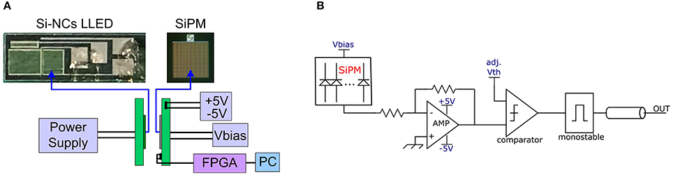
Figure 5. (A) Schematic of the experimental setup with a Si-NCs LLED coupled with a SiPM at a distance of ~ 1 mm. The SiPM board is connected to ±5 V and a bias voltage (Vbias) is applied to the SiPM. The Si-NCs LLED is driven by an applied current (voltage) provided by the power supply. The output signal of the SiPM is transmitted to an FPGA connected to a PC for the generation of random numbers. (B) The front-end board to amplify and digitalize the analog output signal from the detector. This is based on an AD8000 amplifier in a trans-impedance configuration, followed by a comparator with an adjustable voltage threshold (adj.Vth) and a monostable, creating pulses of 3.3 V and 100 ns width.
4. Experimental
The experimental setup is schematically shown in Figure 5A. The (m)LLED is directly facing a SiPM at a distance of ~ 1 mm without any interposed optics or diffuser. The Si-NCs LLED is driven by an Agilent B1500A Semiconductor Device Parameter Analyzer. The TTL output of the SiPM is directly connected to the high speed digital input of an FPGA. A voltage of ~30–36 V is applied to the SiPM by an Agilent E3631A DC Power Supply. The measurement of the arrival times is performed by a fully synchronous logic. The FPGA continuously samples the detector at the frequency of 100 MHz, which is crystal controlled. A valid detection is produced by a high analog logic level heralded by one clock cycle (10 ns) of low analog logic level. A Digilent ATLYS FPGA board has been used with the programming language VHDL.
In order to verify that the Si-NCs emit independent photons, cross correlation measurements can be performed. The measurement is based on the random transmission of the emitted photons from the source (i.e., a Si-NCs LLED) into two arms of a fiber beam splitter (see Figure 6A) each connected to a detector (i.e., a SPAD). The longer arms of the fiber splitter are long enough (15 m) to prevent any possible peaks in the correlogram due to the correlation of either backflashs or back reflections and the real signals on the silicon SPADs within 60 ns time lags. Therefore, any visible peaks in the correlogram would be the result of photon bunching. The output signal of the two detectors are then sent to the two channels of a linear-tau cross-correlator having the time resolution of 1.3 ns, where the cross-correlation function, g2(τ), is computed. A peak in the cross-correlogram indicates photon bunching while a dip shows anti-bunching. Photon bunching occurs in the case of chaotic or thermal light which has a super-Poissonian distribution with the mean greater than the variance and photon number fluctuations larger than in a coherent light beam. Photon antibunching refers to a sub-Poissonian distribution with the mean lower than the variance and photon number fluctuations smaller than in a coherent light beam [11]. A flat cross-correlogram demonstrates that the photons are emitted independently with a Poisson distribution [12]. Measurement results are presented in Figure 6B. As can be seen, a flat cross-correlation graph (with no peak or dip) is observed, which demonstrates that the detected photons follow a Poisson distribution. This is another proof, in addition to the χ2 statistic [6], that the Poisson distribution is a good match for the distribution of the detected photons which are emitted from the Si-NCs LLED.
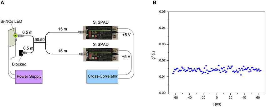
Figure 6. (A) The cross-correlation setup consisting of a 50:50 optical multimode fiber splitter coupled with Si-NCs LED from one of the shorter arms (0.5 m) end and with commerical silicon SPADs from the longer arms (15 m) ends and a linear cross-correlator to perform cross-correlation measurement of the output signals from the silicon SPADs. The other 0.5 m arm is being blocked to light exposure. (B) The cross-correlogram of the output pulses. The flat graph indicates that the detected photons follow a Poisson distribution within the resolution of the instrument. The plot is not normalized and the error bars can be seen for some data points.
In order to characterize afterpulsing and crosstalk in the SiPM, autocorrelation, g2(τ), measurements of its signal were performed via a multitau digital correlator with 4 ns resolution [13]. g2(τ) exhibits a main peak within ~140 ns from the main autocorrelation peak at τ = 0 (Figure 7). The plateau in g2(τ) approaches the normalization value of 1 at about 950 ns.
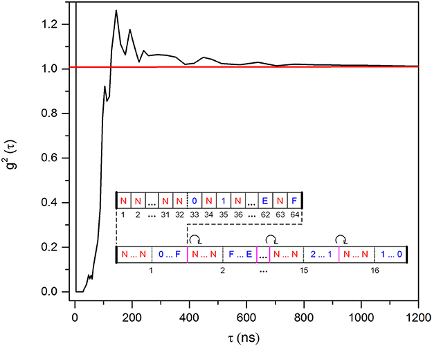
Figure 7. Autocorrelation function (g2(τ)) of the SiPM signal (peak at zero is out of scale). Dead time and afterpulsing distribution of the SiPM can be seen here. The dead time of ~110 ns is not due to limitation of the SiPM, but it is set by the monostable in the electronics (front-end shown in Figure 5B). The inset shows “super interval” which consists of 16 “double length” intervals with first half of no numbers (N) and second half of alternate hexadecimal symbols and Ns (zoomed in above the “super interval”). Consecutive one-rotation of hexadecimal symbols in the second half of the “double length” intervals is indicated by a circular arrow. The inset is taken from Bisadi et al. [9].
The measurements for random number generation were performed on the (m)LLED with an active area of ~ 0.99 mm × 0.82 mm (see Figure 1A) which matches the SiPM dimension of 1 mm × 1 mm. The applied forward current to LLED was kept below ~45 μA corresponding to the forward voltage of 3 V (see Figure 2B) in order to avoid degradation of the oxide layer in the active area of the Si-NCs LLED [14]. The Vbias to SiPM was 32 V corresponding to an excess bias of ~6 V (Vbd = 26V) with the DCR of ~80 kcps/mm2.
The methodology to generate random numbers is similar to our recent work [9]. It is based on the property of the Poisson statistics that, if an event is observed in a time interval T, the probability that the observation is performed in any subinterval of fixed length of T is uniform. Based on this property and to account for the system limitations, we can describe the methodology by defining “double length” periodic time intervals with an associated fully deterministic “target function”. In the case of 16 random number generating subintervals, the alphabet of the symbols is N, 0, 1, …F, that reads N (no-number), and the hexadecimal numbers 0 to F. Each interval has 32 N subintervals in the first half and an alternation of N subintervals and the full set of numeric symbols in the second half, with a total of 64 subintervals (inset of Figure 7). Only if one single detection (event) hits the target function associated with an interval, a random symbol is generated. A mitigation technique is developed in order to improve the non-uniformity in the probability distribution of the generated random symbols. It is called “super interval structure” and is made before the possible arrival of a photon in an interval. As can be seen in the inset of Figure 7, it is composed of 16 “double length” intervals in which the random number generating symbols are ordered as 0, 1,…F in the first interval, F, 0, …E in the second one and so on [9]. This approach results in the nearly uniform probability distribution of the generated symbols (Figure 9).
The duration of the “double length” interval is determined by the afterpulsing and crosstalk distribution of the SiPM (Figure 7). In order to mask the afterpulsing and crosstalk distribution of SiPM, we needed to set the first half of “double length” interval to ~950 ns (see Figure 7). We considered target functions with “super interval” of lengths 640, 1280, and 1920 ns and studied the autocorrelation coefficient of the generated hexadecimal symbols at time lag 1. It is observed to decrease as the length of “super interval” increases with the values of 1.29 × 10⁻⁴, 1.05 × 10⁻⁴ and 1.45 × 10⁻⁵ corresponding to the “double length” interval of 640, 1280, and 1920 ns, respectively. Therefore, we fixed the “double length” interval to 1920 ns and acquired sequences of random symbols.
5. Evaluation of Randomness
A very straightforward way to detect an observable pattern among the random symbols or codes is to create a 2-dimensional map of them. A 512 × 512 map of the 16 hexadecimal symbols generated by our methodology from a recording of our system is presented in Figure 8. As can be seen clearly, no particular, periodic pattern is observed among the symbols.
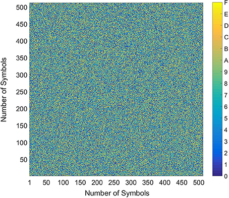
Figure 8. A 512 × 512 map of the hexadecimal symbols. No particular, periodic pattern is observable among the symbols.
Figure 9 shows the probability of generated hexadecimal symbols in a sequence of 1 G symbols. It is seen to follow an uniform distribution (the theoretical value for the probability distribution of 16 bin symbols (1/16) is indicated by a solid red line in Figure 9).
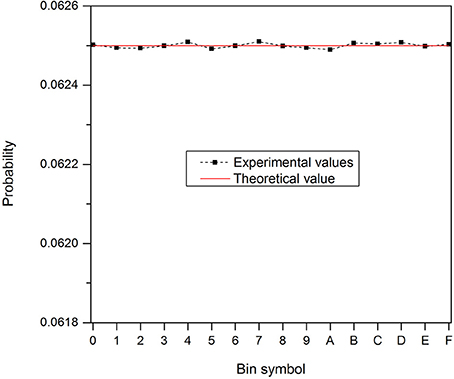
Figure 9. Probability distribution of 16 hexadecimal symbols in a sequence of 1 G symbols raw data. The solid red line shows the theoretical value of 1/16.
The high quality of random symbols is proved through the evaluation of the joint probability mass function (JPMF) [15], which shows a very low deviation of ~5 × 10⁻⁶ from the expected theoretical value of (1/16) × (1/16) = 0.00390625 (Figure 10), and the evaluation of the mutual information (MI) [16], which is calculated to be ~1.5 × 10−7 bits considering 1 G random symbols.
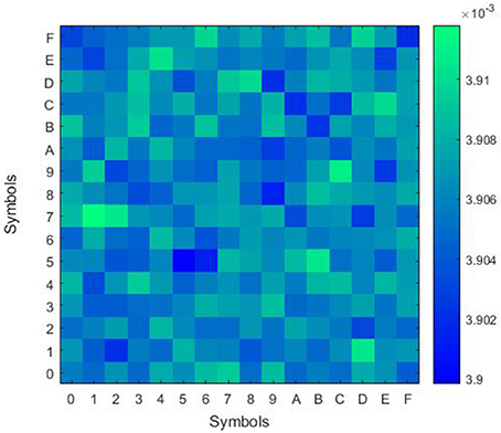
Figure 10. Joint probability mass function for 1 G symbols showing the probability of having each symbol after the other one.
To further analyze the quality of generated random numbers, each symbol is replaced with its corresponding 4-bit binary values. In this way, we obtain a binary sequence of random bits. We then apply the 15 statistical tests in the NIST tests suite to the generated raw data. Various datasets with 1 and 2 Gbits length at different applied currents to the (m)LLED were obtained. They all passed the NIST tests without the application of a post-processing algorithm irrespective of the EL variations of the (m)LLED during data acquisition. The results for a dataset of 2 Gbits are tabulated in Table 2. The highest experimental bit-rate is calculated to be 0.5 Mbps at the EL intensity of ~ 550 Kcps.
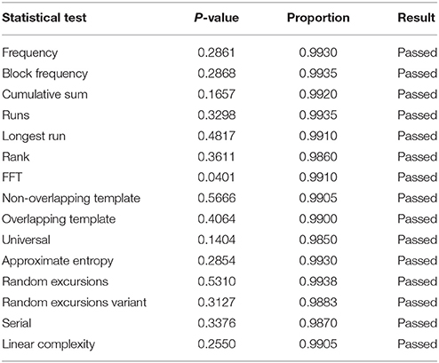
Table 2. NIST tests results for 2 G random bits (2 × 109 bits). The significance level is α = 0.01. In order to pass, the p-value should be larger than 0.01 and the proportion should be more than 0.983.
6. Conclusions
We realized a compact quantum random number generator with a novel configuration comprising a Si-NCs LLED directly interfaced with a SiPM without any coupling optics. This paves the way to the further integration of the photon source and the single photon detectors in a single integrated circuits. Indeed, both the devices were fabricated by using the FBK technology. Our research is currently focusing to define a single fabrication process allowing the fabrication of both devices in a single silicon chip.
Remarkably the Si-NCs LLED have similar emission properties and statistics as the standard small Si-NCs which we have previously developed for PQRNG application [6, 9]. Therefore we could use the same robust methodology to extract high quality random numbers which is implemented on a FPGA. The methodology considers the non-idealities of the detector and the source of photons, including parameters (like EL) drifts. The generated high quality random numbers pass all the statistical tests in NIST tests suite without any post-processing. The highest bit rate is 0.5 Mbps with the efficiency of 4-bits per detected photon.
This compact QRNG, with the capability of producing high quality random numbers, can be implemented in small electronic devices providing utmost security accessible to everyone. The proposed device configuration has several advantage with respect to what we already reported in Bisadi et al. [9], particularly with respect to the simplicity of the system (no optics, no thermoelectrical cooler, simple power supply). Still the proposed device can be further optimized by improving the spectral overlap between the LLED and the SiPM and by increasing the parallelization of the Si-NCs LLED/SiPM which can further improve the bit rate to higher values if required by some applications.
Author Contributions
ZB prepared the setup, conducted the experiments and analyzed the acquired data. She also made some suggestions to adapt the robust methodology to generate high quality random numbers with the structure. FA partially designed the silicon photomultiplier (SiPM) and characterized it. GF created the robust methodology to generate high quality random numbers and implemented the target function on the FPGA. NZ designed most part of the SiPM. CP supervised the development of the technology used in the SiPM. GP designed and fabricated the large area silicon nanocrystals LED (Si-NCs LLED). LP supervised the whole research work.
Conflict of Interest Statement
The authors declare that the research was conducted in the absence of any commercial or financial relationships that could be construed as a potential conflict of interest.
Acknowledgments
This work has been supported by the Provincia Autonoma di Trento via the project “SiQuro.”
Footnotes
1. ^Dataset. http://www.idquantique.com/wordpress/wp-content/uploads/white-paper-understanding-qkd.pdf. (2016).
2. ^Dataset. “http://www.ieee.li/pdf/essay/pin_diode_handbook.pdf/” (1998).
References
1. Hai-Qiang M, Su-Mei W, Da Z, Jun-Tao C, Ling-Ling J, Yan-Xue H, et al. A random number generator based on quantum entangled photon pairs. Chinese Phys Lett. (2004) 21:1961–4. doi: 10.1088/0256-307X/21/10/027
2. Stipčević M, Rogina BM. Quantum random number generator based on photonic emission in semiconductors. Rev Sci Instrum. (2007) 78:045104. doi: 10.1063/1.2720728
3. Stipčević M, Bowers J. Spatio-temporal optical random number generator. Opt Express. (2015) 23:11619–31. doi: 10.1364/OE.23.011619
4. Sanguinetti B, Martin A, Zbinden H, Gisin N. Quantum random number generation on a mobile phone. Phys Rev X. (2014) 4:031056. doi: 10.1103/PhysRevX.4.031056
5. Applegate M, Thomas O, Dynes J, Yuan Z, Ritchie D, Shields A. Efficient and robust quantum random number generation by photon number detection. Appl Phys Lett. (2015) 107:071106. doi: 10.1063/1.4928732
6. Bisadi Z, Meneghetti A, Tomasi A, Tengattini A, Fontana G, Pucker G, et al. Generation of high quality random numbers via an all-silicon-based approach. Phys Status Solidi (2016) 213:3186–93. doi: 10.1002/pssa.201600298
7. Wahl M, Leifgen M, Berlin M, Røhlicke T, Rahn HJ, Benson O. An ultrafast quantum random number generator with provably bounded output bias based on photon arrival time measurements. Appl Phys Lett. (2011) 98:171105. doi: 10.1063/1.3578456
8. Tisa S, Villa F, Giudice A, Simmerle G, Zappa F. High-speed quantum random number generation using CMOS photon counting detectors. IEEE J Sel Top Quantum Electron. (2015) 21:23–9. doi: 10.1109/JSTQE.2014.2375132
9. Bisadi Z, Fontana G, Moser E, Pucker G, Pavesi L. Robust quantum random number generation with silicon nanocrystals light source. J Lightwave Technol. (2017) 35:1588–94. doi: 10.1109/JLT.2017.2656866
10. Acerbi F, Ferri A, Zappala G, Paternoster G, Picciotto A, Gola A, et al. NUV silicon photomultipliers with high detection efficiency and reduced delayed correlated-noise. IEEE Trans Nucl Sci. (2015) 62:1318–25. doi: 10.1109/TNS.2015.2424676
12. Qu D, Dainty J. A Multichannel Detector for Photon Correlation. Adv Electron El Phys. (1988) 74:107–18. doi: 10.1016/S0065-2539(08)60447-3
13. Kalinin S, Kuhnemuth R, Vardanyan H, Seidel CA. Note: A 4 ns hardware photon correlator based on a general-purpose field-programmable gate array development board implemented in a compact setup for fluorescence correlation spectroscopy. Rev Sci Instrum. (2012) 83:096105. doi: 10.1063/1.4753994
14. Marconi A, Anopchenko A, Wang M, Pucker G, Bellutti P, Pavesi L. High power efficiency in Si-nc/SiO2 multilayer light emitting devices by bipolar direct tunneling. Appl Phys Lett. (2009) 94:221110. doi: 10.1063/1.3147164
15. Grimmett G, Stirzaker D. Probability and Random Processes. New York, NY: Oxford University Press (2001).
Keywords: compact photonic quantum random number generation, silicon nanocrystals LED, silicon photomultiplier, robust methodology, NIST tests
Citation: Bisadi Z, Acerbi F, Fontana G, Zorzi N, Piemonte C, Pucker G and Pavesi L (2018) Compact Quantum Random Number Generator with Silicon Nanocrystals Light Emitting Device Coupled to a Silicon Photomultiplier. Front. Phys. 6:9. doi: 10.3389/fphy.2018.00009
Received: 28 September 2017; Accepted: 30 January 2018;
Published: 14 February 2018.
Edited by:
Derek Abbott, University of Adelaide, AustraliaReviewed by:
Junichi Fujikata, Photonics Electronics Technology Research Association, JapanBernard Gelloz, Nagoya University, Japan
Copyright © 2018 Bisadi, Acerbi, Fontana, Zorzi, Piemonte, Pucker and Pavesi. This is an open-access article distributed under the terms of the Creative Commons Attribution License (CC BY). The use, distribution or reproduction in other forums is permitted, provided the original author(s) and the copyright owner are credited and that the original publication in this journal is cited, in accordance with accepted academic practice. No use, distribution or reproduction is permitted which does not comply with these terms.
*Correspondence: Zahra Bisadi, zahra.bisadi@unitn.it; zahra.bisadi.86@gmail.com